ICGOO在线商城 > 射频/IF 和 RFID > RF 调制器 > LTC5598IUF#PBF

 Datasheet下载
- 型号: LTC5598IUF#PBF
- 制造商: LINEAR TECHNOLOGY
- 库位|库存: xxxx|xxxx
- 要求:
| 数量阶梯 | 香港交货 | 国内含税 |
| +xxxx | $xxxx | ¥xxxx |
查看当月历史价格
查看今年历史价格
LTC5598IUF#PBF产品简介:
ICGOO电子元器件商城为您提供LTC5598IUF#PBF由LINEAR TECHNOLOGY设计生产,在icgoo商城现货销售,并且可以通过原厂、代理商等渠道进行代购。 LTC5598IUF#PBF价格参考。LINEAR TECHNOLOGYLTC5598IUF#PBF封装/规格:RF 调制器, RF Modulator IC 5MHz ~ 1.6GHz 24-WFQFN Exposed Pad。您可以下载LTC5598IUF#PBF参考资料、Datasheet数据手册功能说明书,资料中有LTC5598IUF#PBF 详细功能的应用电路图电压和使用方法及教程。
LTC5598(现归于Analog Devices旗下)是一款高性能的RF调制器,广泛应用于无线通信、雷达系统、测试测量设备以及其他需要高线性度和低失真的射频信号处理场景。以下是其主要应用场景:

1. 蜂窝通信基础设施
   LTC5598可用于基站中的上变频器设计,将基带或中频信号转换为射频信号,适用于GSM、CDMA、WCDMA、LTE等通信标准。其优异的线性度和低杂散性能有助于提高信号质量并减少干扰。

2. 点对点微波回传系统
   在无线回传网络中,该器件能够实现高效的数据传输,支持宽带调制格式(如QAM),确保长距离通信的稳定性和可靠性。

3. 卫星通信与地面站设备
   用于卫星通信系统的上行链路信号生成,提供高质量的射频输出以满足严格的频谱纯度要求。

4. 雷达系统
   在脉冲或多普勒雷达中,LTC5598可作为信号调制的核心组件,帮助生成精确的射频波形,提升目标检测能力。

5. 测试与测量仪器
   高端频谱分析仪、信号发生器等设备中使用此芯片来产生纯净的射频信号,以验证其他电子系统的性能。

6. 无线传感器网络及物联网(IoT)应用
   在某些高性能IoT设备中,LTC5598可用于构建高效的射频前端,支持多种无线协议。

7. 军事与航空航天领域
   因其卓越的射频性能和可靠性,该产品也适用于军用通信、导航以及电子对抗系统。

总结来说,LTC5598凭借其宽泛的工作频率范围(高达6GHz)、高动态范围以及紧凑的封装形式,在众多现代射频系统中发挥着关键作用。
| 参数 | 数值 |
| 产品目录 | |
| 描述 | IC MODULATOR QUADRATURE 24-QFN |
| 产品分类 | |
| LO频率 | 5MHz ~ 1.6GHz |
| 品牌 | Linear Technology |
| 数据手册 | http://www.linear.com/docs/27936 |
| 产品图片 |
|
| P1dB | 8.5dBm |
| 产品型号 | LTC5598IUF#PBF |
| RF频率 | 5MHz ~ 1.6GHz |
| rohs | 无铅 / 符合限制有害物质指令(RoHS)规范要求 |
| 产品系列 | - |
| 产品目录页面 | |
| 其它名称 | LTC5598IUFPBF |
| 功能 | 调制器 |
| 包装 | 管件 |
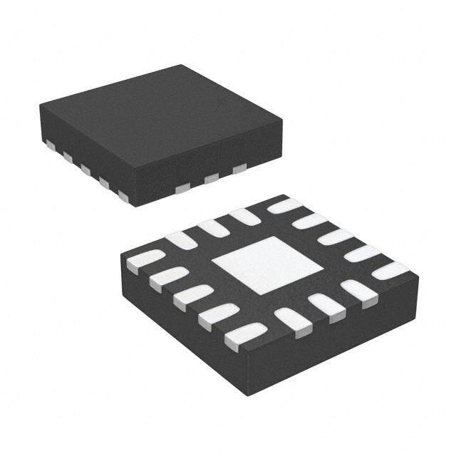
| 封装/外壳 | 24-WFQFN 裸露焊盘 |
| 本底噪声 | -160.3dBm/Hz |
| 标准包装 | 91 |
| 测试频率 | 899.9MHz |
| 电压-电源 | 4.5 V ~ 5.25 V |
| 电流-电源 | 200mA |
| 输出功率 | 2dBm |


- 商务部:美国ITC正式对集成电路等产品启动337调查
- 曝三星4nm工艺存在良率问题 高通将骁龙8 Gen1或转产台积电
- 太阳诱电将投资9.5亿元在常州建新厂生产MLCC 预计2023年完工
- 英特尔发布欧洲新工厂建设计划 深化IDM 2.0 战略
- 台积电先进制程称霸业界 有大客户加持明年业绩稳了
- 达到5530亿美元!SIA预计今年全球半导体销售额将创下新高
- 英特尔拟将自动驾驶子公司Mobileye上市 估值或超500亿美元
- 三星加码芯片和SET,合并消费电子和移动部门,撤换高东真等 CEO
- 三星电子宣布重大人事变动 还合并消费电子和移动部门
- 海关总署:前11个月进口集成电路产品价值2.52万亿元 增长14.8%


PDF Datasheet 数据手册内容提取
LTC5598 5MHz to 1600MHz High Linearity Direct Quadrature Modulator FEATURES DESCRIPTION n Frequency Range: 5MHz to 1600MHz The LTC®5598 is a direct I/Q modulator designed for high n High Output IP3: +27.7dBm at 140MHz performance wireless applications, including wireless +22.9dBm at 900MHz infrastructure. It allows direct modulation of an RF signal n Low Output Noise Floor at 6MHz Offset: using differential baseband I and Q signals. It supports No Baseband AC Input: –161.2dBm/Hz point-to-point microwave link, GSM, EDGE, CDMA, POUT = 5.5dBm: –160dBm/Hz 700MHz band LTE, CDMA2000, CATV applications and n Low LO Feedthrough: –55dBm at 140MHz other systems. It may also be confi gured as an image n High Image Rejection: –50.4dBc at 140MHz reject upconverting mixer, by applying 90° phase-shifted n Integrated LO Buffer and LO Quadrature Phase signals to the I and Q inputs. Generator The I/Q baseband inputs consist of voltage-to-current n 50Ω Single-Ended LO and RF Ports converters that in turn drive double-balanced mixers. n >400MHz Baseband Bandwidth The outputs of these mixers are summed and applied n 24-Lead QFN 4mm × 4mm Package to a buffer, which converts the differential mixer signals n Pin-Compatible with Industry Standard Pin-Out to a 50Ω single-ended buffered RF output. The four n Shut-down Mode balanced I and Q baseband input ports are intended for APPLICATIONS DC coupling from a source with a common-mode voltage level of about 0.5V. The LO path consists of an LO buffer n Point-to-Point Microwave Link with single-ended or differential inputs, and precision n Military Radio quadrature generators that produce the LO drive for the n Basestation Transmitter GSM/EDGE/CDMA2K mixers. The supply voltage range is 4.5V to 5.25V, with n 700MHz LTE Basestation Transmitter about 168mA current. n Satellite Communication L, LT, LTC and LTM are registered trademarks of Linear Technology Corporation. n CATV/Cable Broadband Modulator All other trademarks are the property of their respective owners. n 13.56MHz/UHF RFID Modulator TYPICAL APPLICATION Noise Floor vs RF Output Power 5MHz to 1600MHz Direct Conversion Transmitter Application and Differential LO Input Power 5V VCC LTC55981xn2F 4x2.7μF m/Hz)–152 fLO = 14200MdHBzm; fBB = 2kHz; CW (NOTE 3) I-DAC V-I RF = 5MHz dB–154 19.3dBm TO 1600MHz T ( 13.4dBm I-CHANNEL SE 10.4dBm EN 0(cid:111) PA Hz OFF–156 86..44ddBBmm 90(cid:111) M Q-CHANNEL 10nF AT 6–158 R Q-DAC V-I OO L E F–160 BASEBAND 5598 TA01 OIS GENERATOR 10nF N –162 50Ω 10nF 470nF –14–12–10–8 –6 –4 –2 0 2 4 6 8 VCO/SYNTHESIZER RF OUTPUT POWER (dBm) 5598 TA02 5598f 1
LTC5598 ABSOLUTE MAXIMUM RATINGS PIN CONFIGURATION (Note 1) Supply Voltage .........................................................5.6V TOP VIEW Common Mode Level of BBPI, BBMI and BBPQ, BBMQ ...........................................................0.6V VCC1 GND BBMI BBPI GND GND 24 23 22 21 20 19 LOP, LOM Input ....................................................20dBm Voltage on Any Pin EN 1 18 VCC2 GND 2 17 GNDRF Not to Exceed ...................................–0.3V to V + 0.3V CC LOP 3 16 RF T ....................................................................150°C 25 JMAX LOM 4 15 NC Operating Temperature Range..................–40°C to 85°C GND 5 14 GNDRF Storage Temperature Range ...................–65°C to 150°C CAPA 6 13 NC 7 8 9 10 11 12 B D Q Q D D P N M P N N CA G BB BB G G UF PACKAGE 24-LEAD (4mm (cid:115) 4mm) PLASTIC QFN TJMAX = 150°C, θJA = 37°C/W EXPOSED PAD (PIN 25) IS GND, MUST BE SOLDERED TO PCB ORDER INFORMATION LEAD FREE FINISH TAPE AND REEL PART MARKING PACKAGE DESCRIPTION TEMPERATURE RANGE LTC5598IUF#PBF LTC5598IUF#TRPBF 5598 24-Lead (4mm × 4mm) Plastic QFN –40°C to 85°C Consult LTC Marketing for parts specifi ed with wider operating temperature ranges. Consult LTC Marketing for information on non-standard lead based fi nish parts. For more information on lead free part marking, go to: http://www.linear.com/leadfree/ For more information on tape and reel specifi cations, go to: http://www.linear.com/tapeandreel/ 5598f 2
LTC5598 ELECTRICAL CHARACTERISTICS V = 5V, EN = 5V, T = 25ºC, P = 0dBm, single-ended; BBPI, BBMI, CC A LO BBPQ, BBMQ common-mode DC voltage V = 0.5V , I&Q baseband input signal = 100kHz CW, 0.8V each, I&Q 90° shifted CMBB DC PP,DIFF (lower side-band selection), unless otherwise noted. (Note 11) SYMBOL PARAMETER CONDITIONS MIN TYP MAX UNITS RF OUTPUT (RF) f RF Frequency Range 5 to 1600 MHz RF S RF Output Return Loss EN = High, 5MHz to 1600MHz <–20 dB 22, ON f = 140MHz, f = 139.9MHz LO RF G Conversion Voltage Gain 20 • Log (V /V ) –2 dB V RF, OUT, 50Ω IN, DIFF, I or Q P Absolute Output Power 1V on each I&Q Inputs 2 dBm OUT PP,DIFF OP1dB Output 1dB Compression 8.5 dBm OIP2 Output 2nd Order Intercept (Notes 4, 5) 74 dBm OIP3 Output 3rd Order Intercept (Notes 4, 6) 27.7 dBm NFloor RF Output Noise Floor No Baseband AC Input Signal (Note 3) –161.2 dBm/Hz P = 4.6dBm (Note 3) P = 10dBm –154.5 dBm/Hz OUT LO, SE P = 5.5dBm (Note 3) P = 20dBm –160 dBm/Hz OUT LO, DIFF IR Image Rejection (Note 7) –50.4 dBc LOFT LO Feedthrough EN = High (Note 7) –55 dBm (Carrier Leakage) EN = Low (Note 7) –78 dBm f = 450MHz, f = 449.9MHz LO RF G Conversion Voltage Gain 20 • Log (V /V ) –5.0 –2.1 0.5 dB V RF, OUT, 50Ω IN, DIFF, I or Q P Absolute Output Power 1V on each I&Q Inputs 1.9 dBm OUT PP,DIFF OP1dB Output 1dB Compression 8.4 dBm OIP2 Output 2nd Order Intercept (Notes 4, 5) 72 dBm OIP3 Output 3rd Order Intercept (Notes 4, 6) 25.5 dBm NFloor RF Output Noise Floor No Baseband AC Input Signal (Note 3) –160.9 dBm/Hz IR Image Rejection (Note 7) –55 dBc LOFT LO Feedthrough EN = High (Note 7) –51 dBm (Carrier Leakage) EN = Low (Note 7) –68 dBm f = 900MHz, f = 899.9MHz LO RF G Conversion Voltage Gain 20 • Log (V /V ) –2 dB V RF, OUT, 50Ω IN, DIFF, I or Q P Absolute Output Power 1V on each I&Q Inputs 2 dBm OUT PP,DIFF OP1dB Output 1dB Compression 8.5 dBm OIP2 Output 2nd Order Intercept (Notes 4, 5) 69 dBm OIP3 Output 3rd Order Intercept (Notes 4, 6) 22.9 dBm NFloor RF Output Noise Floor No Baseband AC Input Signal (Note 3) –160.3 dBm/Hz P = 5.2dBm (Note 3) P = 10dBm –154.5 dBm/Hz OUT LO, SE IR Image Rejection (Note 7) –54 dBc LOFT LO Feedthrough EN = High (Note 7) –48 dBm (Carrier Leakage) EN = Low (Note 7) –54 dBm 5598f 3
LTC5598 ELECTRICAL CHARACTERISTICS V = 5V, EN = 5V, T = 25ºC, P = 0dBm, single-ended; BBPI, BBMI, CC A LO BBPQ, BBMQ common-mode DC voltage V = 0.5V , I&Q baseband input signal = 100kHz CW, 0.8V each, I&Q 90° shifted CMBB DC PP,DIFF (lower side-band selection), unless otherwise noted. (Note 11) SYMBOL PARAMETER CONDITIONS MIN TYP MAX UNITS LO INPUT (LOP) f LO Frequency Range 5 to 1600 MHz LO P Differential LO Input Power Range –10 to 20 dBm LO,DIFF P Single-Ended LO Input Power Range –10 to 12 dBm LO, SE S LO Input Return Loss EN = High –10.5 dB 11, ON S LO Input Return Loss EN = Low –9.6 dB 11, OFF BASEBAND INPUTS (BBPI, BBMI, BBPQ, BBMQ) BW Baseband Bandwidth -3dB Bandwidth >400 MHz BB I Baseband Input Current Single-Ended –68 μA b,BB R Input Resistance Single-Ended –7.4 kΩ IN, SE V DC Common-Mode Voltage Externally Applied 0.5 V CMBB V Amplitude Swing No Hard Clipping, Single-Ended 0.86 V SWING P-P POWER SUPPLY (V , V ) CC1 CC2 V Supply Voltage 4.5 5 5.25 V CC I Supply Current EN = High, I + I 130 165 200 mA CC(ON) CC1 CC2 I Supply Current, Sleep Mode EN = 0V, I + I 0.24 0.9 mA CC(OFF) CC1 CC2 t Turn-On Time EN = Low to High (Notes 8, 10) 75 ns ON t Turn-Off Time EN = High to Low (Notes 9, 10) 10 ns OFF POWER UP/DOWN Enable Input High Voltage EN = High 2 V Input High Current EN = 5V 43 μA Sleep Input Low Voltage EN = Low 1 V Input Low Current EN = 0V –40 μA Note 1: Stresses beyond those listed under Absolute Maximum Ratings Note 6: IM3 is measured at LO frequency – 1.9 MHz and LO frequency may cause permanent damage to the device. Exposure to any Absolute – 2.2MHz. Maximum Rating condition for extended periods may affect device Note 7: Amplitude average of the characterization data set without image reliability and lifetime. or LO feedthrough nulling (unadjusted). Note 2: The LTC5598 is guaranteed functional over the operating Note 8: RF power is within 10% of fi nal value. temperature range –40ºC to 85ºC. Note 9: RF power is at least 30dB lower than in the ON state. Note 3: At 6MHz offset from the LO signal frequency. 100nF between BBPI Note 10: External coupling capacitors at pins LOP, LOM and RF are 100pF and BBMI, 100nF between BBPQ and BBMQ. each. Note 4: Baseband is driven by 2MHz and 2.1MHz tones with 1V for PP,DIFF Note 11: Tests are performed as shown in the confi guration of Figure 10. two-tone signals at each I or Q input (0.5V for each tone). PP,DIFF The LO power is applied to J3 while J5 is terminated with 50Ω to ground Note 5: IM2 is measured at LO frequency – 4.1MHz. for single-ended LO drive. 5598f 4
LTC5598 TYPICAL PERFORMANCE CHARACTERISTICS V = 5V, EN = 5V, T = 25ºC, f = f – f , P = CC A RF LO BB LO 0dBm single-ended, BBPI, BBMI, BBPQ, BBMQ common-mode DC voltage V = 0.5V , I&Q baseband input signal = 100kHz, CMBB DC 0.8V , two-tone baseband input signal = 2MHz, 2.1MHz, 0.5V each tone, I&Q 90° shifted (lower side-band selection); PP,DIFF PP,DIFF f = f – 6MHz; unless otherwise noted. (Note 11) NOISE LO Supply Current vs Temperature Voltage Gain vs RF Frequency Output IP3 vs RF Frequency 180 –1 29 5.25V 27 A) 170 –2 NT (m 5.0V N (dB) m) 25 CURRE 160 GE GAI –3 P3 (dB 23 UPPLY VOLTA 5V, 25°C OI 21 5V, 25°C S 150 4.5V –4 5.25V, 25°C 5.25V, 25°C 4.5V, 25°C 19 4.5V, 25°C 5V, –40°C 5V, –40°C 5V, 85°C 5V, 85°C 140 –5 17 –40 –15 10 35 60 85 10 100 1000 10 100 1000 TEMPERATURE (°C) RF FREQUENCY (MHz) RF FREQUENCY (MHz) 5598 G02 5598 G03 5598 G01 Output 1dB Compression LO Feedthrough to RF Output Output IP2 vs RF Frequency vs RF Frequency vs LO Frequency 85 10 –40 80 8 m) B 75 d –50 OIP2 (dBm) 7605 OP1dB (dBm) 64 EEDTHROUGH ( –60 5V, 25°C 5V, 25°C O F 5V, 25°C 5.25V, 25°C 5.25V, 25°C L 5.25V, 25°C 60 4.5V, 25°C 2 4.5V, 25°C 4.5V, 25°C 5V, –40°C 5V, –40°C 5V, –40°C 5V, 85°C 5V, 85°C 5V, 85°C 55 0 –70 10 100 1000 10 100 1000 10 100 1000 RF FREQUENCY (MHz) RF FREQUENCY (MHz) LO FREQUENCY (MHz) 5598 G04 5598 G05 5598 G06 Noise Floor vs RF Frequency RF Two-Tone Power (Each Tone), Image Rejection vs LO Frequency (No AC Baseband Input Signal) IM2 and IM3 vs RF Frequency –20 –145 0 –40 5V, 25°C 5V, 25°C 5.25V, 25°C 5.25V, 25°C fRF, EACH = fLO – fBB1 4.5V, 25°C 4.5V, 25°C –10 –50 –30 GE REJECTION (dBc) ––4500 55VV,, –8450°C°C SE FLOOR (dBm/Hz)––115550 55(NVV,O, –8T45E0° 3C°)C P (dBm)RF,TONE–––432000 fIM3 = fLOf I–M 32 *=f BfLBO1 ++ f2B*Bf2BB1+fBB2 –––876000 IM2 (dBm), IM3 (dB IMA NOI–160 m) –60 –50 fIM2 = fLO – fBB1–fBB2 –90 –70 –165 –60 –100 10 100 1000 10 100 1000 10 100 1000 LO FREQUENCY (MHz) RF FREQUENCY (MHz) RF FREQUENCY (MHz) 5598 G07 5598 G08 5598 G09 5598f 5
LTC5598 TYPICAL PERFORMANCE CHARACTERISTICS V = 5V, EN = 5V, T = 25ºC, f = f – f , P = CC A RF LO BB LO 0dBm single-ended, BBPI, BBMI, BBPQ, BBMQ common-mode DC voltage V = 0.5V , I&Q baseband input signal = 100kHz, CMBB DC 0.8V , two-tone baseband input signal = 2MHz, 2.1MHz, 0.5V each tone, I&Q 90° shifted (lower side-band selection); PP,DIFF PP,DIFF f = f – 6MHz; unless otherwise noted. (Note 11) NOISE LO RF Two-Tone Power (Each Tone), RF Two-Tone Power (Each Tone), IM2 and IM3 vs Baseband Voltage IM2 and IM3 vs Baseband Voltage Voltage Gain vs RF Frequency and Temperature (f = 140MHz) and Temperature (f = 900MHz) (P = 10dBm) LO LO LO 10 –30 10 –30 –1 PLO = 10dBm 0 –40 0 fRF, EACH = fLO – fBB1 –40 –2 P (dBm)RF, TONE–––321000 ffffRIIIMMMF,332 E A===C fffHLLLOOO = –+–f L22fOB** B–ff1BBfBBB–B11f1B++Bff2BBBB22 –––765000 IM2 (dBm), IM3 (dBm P (dBm)RF,TONE–––321000 fIM3 =fI MfL3O = – f L2O* f+B B21*+fBfBB1B+2fBB2 –––765000 IM2 (dBm), IM3 (dBm VOLTAGE GAIN (dB)–3 5V, 25°C ) ) –4 5.25V, 25°C –40 –80 –40 fIM2 = fLO – fBB1–fBB2 –80 4.5V, 25°C 5V, –40°C 5V, 85°C –50 –90 –50 –90 –5 0.1 1 0.1 1 10 100 1000 I AND Q BASEBAND VOLTAGE (VPP, DIFF, EACH TONE) I AND Q BASEBAND VOLTAGE (VPP, DIFF, EACH TONE) RF FREQUENCY (MHz) 5598 G10 5598 G11 5598 G12 Output IP3 vs RF Frequency Output IP2 vs RF Frequency Output 1dB Compression (P = 10dBm) (P = 10dBm) vs RF Frequency (P = 10dBm) LO LO LO 29 85 10 27 80 8 25 75 OIP3 (dBm) 23 OIP2 (dBm) 70 OP1dB (dBm) 64 21 65 5V, 25°C 5V, 25°C 5V, 25°C 5.25V, 25°C 5.25V, 25°C 5.25V, 25°C 2 19 4.5V, 25°C 60 4.5V, 25°C 4.5V, 25°C 5V, –40°C 5V, –40°C 5V, –40°C 5V, 85°C 5V, 85°C 5V, 85°C 17 55 0 10 100 1000 10 100 1000 10 100 1000 RF FREQUENCY (MHz) RF FREQUENCY (MHz) RF FREQUENCY (MHz) 5598 G13 5598 G14 5598 G15 RF Two-Tone Power (Each Tone), LO Feedthrough to RF Output Image Rejection vs LO Frequency IM2 and IM3 vs RF Frequency vs LO Frequency (P = 10dBm) (P = 10dBm) (P = 10dBm) LO LO LO –40 –20 0 –40 5V, 25°C 5.25V, 25°C fRF, EACH = fLO – fBB1 4.5V, 25°C –30 EEDTHROUGH (dBm) ––5600 GE REJECTION (dBc) ––4500 55VV,, –8450°C°C P (dBm)RF, TONE fIM3 = ffLIMO 3– = 2 f*LfOB B+1 2+*ffBBBB21+fBB2 IM2 (dBm), IM3 (dB O F 5V, 25°C MA m) L 5.25V, 25°C I –60 4.5V, 25°C fIM2 = fLO – fBB1–fBB2 5V, –40°C 5V, 85°C –70 –70 –60 –100 10 100 1000 10 100 1000 10 100 1000 LO FREQUENCY (MHz) LO FREQUENCY (MHz) RF FREQUENCY (MHz) 5598 G16 5598 G17 5598 G18 5598f 6
LTC5598 TYPICAL PERFORMANCE CHARACTERISTICS V = 5V, EN = 5V, T = 25ºC, f = f – f , f CC A RF LO BB LO = 450MHz, P = 0dBm single-ended, BBPI, BBMI, BBPQ, BBMQ common-mode DC voltage V = 0.5V , I&Q baseband input signal LO CMBB DC = 100kHz, 0.8V , two-tone baseband input signal = 2MHz, 2.1MHz, 0.5V each tone, I&Q 90° shifted (lower side-band PP,DIFF PP,DIFF selection); f = f – 6MHz; unless otherwise noted. (Note 11) NOISE LO Noise Floor vs RF Frequency (P = 10dBm, No AC Baseband LO Feedthrough to RF Output Image Rejection vs LO Frequency LO Input Signal) vs LO Frequency for EN = Low (P = 10dBm) LO –145 0 5V, 25°C 5.25V, 25°C –40 –10 4.5V, 25°C –40°C C8 = 0 Bm/Hz)–150 55(NVV,O, –8T45E0° 3C°)C H (dBm) –60 N (dBc)––3200 d G O OR (–155 ROU –80 PLO = 10dBm ECTI–40 E FLO EDTH–100 E REJ–50 NOIS–160 LO FE PLO = 0dBm 85°C IMAG–60 C8 = 470nF –120 –70 –165 –140 –80 10 100 1000 10 100 1000 10 100 1000 RF FREQUENCY (MHz) LO FREQUENCY (MHz) LO FREQUENCY (MHz) 5598 G19 5598 G20 5598 G20a Noise Floor vs RF Output Power and Differential LO Input Power Gain Distribution Output IP3 Distribution at 25°C –152 60 30 Hz) fLO = 140MHz; fBB = 2kHz; CW (NOTE 3) 8255(cid:111)(cid:111)CC m/ 50 –40(cid:111)C 25 B–154 20dBm d T ( 19.3dBm SE 13.4dBm %) 40 %) 20 OFF–156 10.4dBm E ( E ( MHz 86..44ddBBmm NTAG 30 NTAG 15 T 6–158 CE CE A R R OR PE 20 PE 10 O L SE F–160 10 5 OI N –162 0 0 –14–12–10 –8 –6 –4 –2 0 2 4 6 8 –2.4 –2.3 –2.2 –2.1 –2 –1.9 24 24.4 24.8 25.2 25.6 26 26.4 26.8 27.2 RF OUTPUT POWER (dBm) GAIN (dB) OIP3 (dBm) 5598 G20b 5598 G21 5598 G22 LO Feedthrough Distribution Image Rejection Distribution Noise Floor Distribution 25 40 70 85(cid:111)C 85(cid:111)C 85(cid:111)C 2–54(cid:111)0C(cid:111)C 35 2–54(cid:111)0C(cid:111)C 60 2–54(cid:111)0C(cid:111)C 20 NO RF 30 50 %) %) %) GE ( 15 GE ( 25 GE ( 40 TA TA 20 TA N N N RCE 10 RCE 15 RCE 30 E E E P P P 20 10 5 5 10 0 0 0 –70 –66 –62 –58 –54 –50 –46 –42 –38 –70 –66 –62 –58 –54 –50 –46 –42 –162.4 –162 –161.6–161.2–160.8–160.4 –160 LO FEEDTHROUGH (dBm) IMAGE REJECTION (dBc) NOISE FLOOR (dBm/Hz) 5598 G23 5598 G24 5598 G25 5598f 7
LTC5598 PIN FUNCTIONS EN (Pin 1): Enable Input. When the Enable Pin voltage is NC (Pins 13, 15): No Connect. These pins are fl oating. higher than 2 V, the IC is turned on. When the input voltage GNDRF (Pins 14, 17): Ground. Pins 14 and 17 are connected is less than 1 V, the IC is turned off. If not connected, the to each other internally and function as the ground return for IC is enabled. the RF output buffer. They are connected via back-to-back GND (Pins 2, 5, 8, 11, 12, 19, 20, 23 and 25): Ground. diodes to the exposed pad 25. For best LO suppression Pins 2, 5, 8, 11, 12, 19, 20, 23 and exposed pad 25 are performance those pins should be grounded separately connected to each other internally. For best RF performance, from the exposed paddle 25. For best RF performance, pins 2, 5, 8, 11, 12, 19, 20, 23 and the Exposed Pad 25 pins 14 and 17 should be connected to RF ground. should be connected to RF ground. RF (Pin 16): RF Output. The RF output is a DC-coupled LOP (Pin 3): Positive LO Input. This LO input is internally single-ended output with approximately 50Ω output biased at about 2.3V. An AC de-coupling capacitor should impedance at RF frequencies. An AC coupling capacitor be used at this pin to match to an external 50Ω source. should be used at this pin to connect to an external load. LOM (Pin 4): Negative LO Input. This input is internally biased at about 2.3V. An AC de-coupling capacitor should be used at V (Pins 18, 24): Power Supply. It is recommended to CC this pin via a 50Ω to ground for best OIP2 performance. use 1nF and 4.7μF capacitors for decoupling to ground on each of these pins. CAPA, CAPB (Pins 6, 7): External capacitor pins. A cap- acitor between the CAPA and the CAPB pin can be used in BBPI, BBMI (Pins 21, 22): Baseband Inputs for the Q- order to improve the image rejection for frequencies below channel, each high input impedance. They should be 100MHz. A capacitor value of 470nF is recommended. externally biased at 0.5V common-mode level and not be These pins are internally biased at about 2.3V. left fl oating. Applied common-mode voltage must stay below 0.6V . BBMQ, BBPQ (Pins 9, 10): Baseband Inputs for the DC Q-channel, each high input impedance. They should be Exposed Pad (Pin 25): Ground. This pin must be soldered externally biased at 0.5V common-mode level and not be to the printed circuit board ground plane. left fl oating. Applied common-mode voltage must stay below 0.6V . DC BLOCK DIAGRAM GND VCC1 VCC2 NC 20 23 25 24 18 13 15 LTC5598 BBPI 21 V-I BBMI 22 0(cid:111) 16 RF EN 1 90(cid:111) BBPQ 10 14 V-I GNDRF BBMQ 9 17 2 5 8 11 3 4 6 7 12 19 5598 BD GND LOP LOM CAPA CAPB GND 5598f 8
LTC5598 APPLICATIONS INFORMATION The LTC5598 consists of I and Q input differential voltage- inserted in each of the four baseband connections, the to-current converters, I and Q up-conversion mixers, an –1dB baseband bandwidth increases to about 800MHz. RF output buffer, an LO quadrature phase generator and It is recommended to include the baseband input impedance LO buffers. in the baseband lowpass fi lter design. The input impedance External I and Q baseband signals are applied to the of each baseband input is given in Table 1. differential baseband input pins, BBPI, BBMI, and BBPQ, Table 1. Single-Ended BB Port Input Impedance vs Frequency BBMQ. These voltage signals are converted to currents and for EN = High and V = 0.5V CMBB DC translated to RF frequency by means of double-balanced FREQUENCY BB INPUT REFLECTION COEFFICIENT up-converting mixers. The mixer outputs are combined (MHz) IMPEDANCE MAG ANGLE in an RF output buffer, which also transforms the output 0.1 –10578 – j263 1.01 –0.02 impedance to 50Ω. The center frequency of the resulting 1 –8436 – j1930 1.011 –0.15 RF signal is equal to the LO signal frequency. The LO input 2 –6340 – j3143 1.013 –0.36 drives a phase shifter which splits the LO signal into in- phase and quadrature LO signals. These LO signals are then 4 –3672 – j3712 1.014 –0.78 applied to on-chip buffers which drive the up-conversion 8 –1644 – j2833 1.015 –1.51 mixers. In most applications, the LOP input is driven by 16 –527 – j1765 1.016 –2.98 the LO source via an optional matching network, while 30 –177 – j1015 1.017 –5.48 the LOM input is terminated with 50Ω to RF ground via 60 –45.2 – j514 1.017 –11 a similar optional matching network. The RF output is 100 –13.2 – j306 1.014 –18.5 single-ended and internally 50Ω matched. 140 –0.2 – j219 1 –25.7 200 4.5 – j151 0.982 –36.6 Baseband Interface 300 10.4 – j99.4 0.921 –52.9 The circuit is optimized for a common mode voltage of 400 12.3 – j72.4 0.854 –68.2 0.5V which should be externally applied. The baseband 500 14.7 – j57.5 0.780 –79.9 pins should not be left fl oating because the internal 600 15.5 – j46.3 0.720 –91.4 PNP’s base current will pull the common mode voltage The baseband inputs should be driven differentially; higher than the 0.6V limit. This condition may damage otherwise, the even-order distortion products may degrade the part. In shut-down mode, it is recommended to have the overall linearity performance. Typically, a DAC will a termination to ground or to a 0.5V source with a value lower than 1kΩ. The PNP’s base current is about –68μA LTC5598 in normal operation. VCC2 = 5V BUFFER RF The baseband inputs (BBPI, BBMI, BBPQ, BBMQ) present VCC1 = 5V a single-ended input impedance of about –7.4kΩ each. FROM Q Because of the negative input impedance, it is important LOMI LOPI to keep the source resistance at each baseband input low enough such that the parallel value remains positive vs BBPI 30Ω baseband frequency. At each of the four baseband inputs, a 4pF capacitor of 4pF in series with 30Ω is connected to ground. VCMBB = 0.5VDC 4pF This is in parallel with a PNP emitter follower (see Figure 1). 30Ω BBMI The baseband bandwidth depends on the source impedance. GNDRF For a 25Ω source impedance, the baseband bandwidth 55682 F01 GND (–1dB) is about 300MHz. If a 5.6nH series inductor is Figure 1. Simplifi ed Circuit Schematic of the LTC5598 (Only I-Half is Drawn) 5598f 9
LTC5598 APPLICATIONS INFORMATION be the signal source for the LTC5598. A reconstruction in Table 3. In Table 4 and 5, the LOP port input impedance fi lter should be placed between the DAC output and the is given for EN = High and Low under the condition of LTC5598’s baseband inputs. P = 10dBm. Figure 4 shows the LOP port return loss LO for the standard demo board (schematic is shown in In Figure 2 a typical baseband interface is shown, using Figure 10) when the LOM port is terminated with 50Ω to a fi fth-order lowpass ladder fi lter. GND. The values of L1, L2, C9 and C10 are chosen such 0mA TO 20mA L1A L2A 0.5VDC BBPI that the bandwidth for the LOP port of the standard demo board is maximized while meeting the LO input return loss R1A R2A 100(cid:55) 100(cid:55) S < –10dB. DAC C1 C2 C3 11, ON R1B R2B 100(cid:55) L1B L2B 100(cid:55) Table 2. LOP Port Input Impedance vs Frequency for EN = High 0mA TO 20mA 0.5VDC BBMI and PLO = 0dBm (LOM AC Coupled With 50Ω to Ground). GND 5598 F02 FREQUENCY LO INPUT REFLECTION COEFFICIENT (MHz) IMPEDANCE MAG ANGLE Figure 2. Baseband Interface with 5th Order Filter and 0.5V DAC (Only I Channel is Shown) 0.1 333 – j10.0 0.739 –0.5 CM 1 318 – j59.9 0.737 –3.3 For each baseband pin, a 0 to 1V swing is developed 2 285 – j94.7 0.728 –6.1 corresponding to a DAC output current of 0mA to 20mA. 4 227 – j120 0.708 –10.6 The maximum sinusoidal single side-band RF output power 8 154 – j124 0.678 –18.7 is about +7.3dBm for full 0V to 1V swing on each I- and 16 89.9 – j95.4 0.611 –33.0 Q- channel baseband input (2V ). PP, DIFF 30 60.4 – j60.6 0.420 –41.3 LO Section 60 54.8 – j35.8 0.489 –51.5 100 43.6 – j24.4 0.261 –89.9 The internal LO chain consists of poly-phase phase shifters 200 37.9 – j17.3 0.235 –113 followed by LO buffers. The LOP input is designed as a 400 31.8 – j12.4 0.266 –137 single-ended input with about 50Ω input impedance. The 800 23.6 – j8.2 0.374 –156 LOM input should be terminated with 50Ω through a DC 1000 19.8 – j5.5 0.437 –165 blocking capacitor. 1250 16.0 – j1.8 0.515 –175 The LOP and LOM inputs can be driven differentially in 1500 13.6 + j2.4 0.574 174 case an exceptionally low large-signal output noise fl oor 1800 12.1 + j7.3 0.618 162 is required (see graph 5598 G20b). VCC1 A simplifi ed circuit schematic for the LOP, LOM, CAPA and CAPB inputs is given in Figure 3. A feedback path is implemented from the LO buffer outputs to the LO inputs in order to minimize offsets in the LO chain by storing the offsets on C5, C7 and C8 (see Figure 10). Optional capacitor LOP LOM CAPB C8 improves the image rejection below 100MHz (see graph 5598 G20a). Because of the feedback path, the input CAPA impedance for P = 0dBm is somewhat different than + LO 2.8V for P = 10dBm for the lower part of the operating (4.3V IN LO SHUTDOWN) frequency range. In Table 2, the LOP port input impedance 5598 F03 vs frequency is given for EN = High and P = 0dBm. For LO EN = Low and P = 0dBm, the input impedance is given Figure 3. Simplifi ed Circuit Schematic for the LO LOP, LOM, CAPA and CAPB Inputs. 5598f 10
LTC5598 APPLICATIONS INFORMATION Table 3. LOP Port Input Impedance vs Frequency for EN = Low Table 5. LOP Port Input Impedance vs Frequency for EN = Low and P = 0dBm (LOM AC Coupled with 50Ω to Ground). and P = 10dBm (LOM AC Coupled with 50Ω to Ground). LO LO FREQUENCY LO INPUT REFLECTION COEFFICIENT FREQUENCY LO INPUT REFLECTION COEFFICIENT (MHz) IMPEDANCE MAG ANGLE (MHz) IMPEDANCE MAG ANGLE 0.1 1376 – j84.4 0.930 –0.3 0.1 454 – j30.5 0.802 –0.9 1 541 – j1593 0.980 –3.2 1 423 – j102 0.780 –3.2 2 177 – j877 0.977 –6.2 2 365 – j165 0.796 –5.9 4 75.3 – j452 0.965 –12.2 4 249 – j219 0.798 –11.4 8 49.2 – j228 0.918 –23.6 8 117 – j179 0.781 –22.4 16 43.3 – j117 0.784 –41.8 16 60.7 – j106 0.697 –40.3 30 40.7 – j64.1 0.585 –62.7 30 43.1 – j62.0 0.559 –62.4 60 39.1 – j34.6 0.382 –86 60 38.6 – j34.6 0.386 –86.7 100 37.6 – j23.8 0.296 –102 100 37.6 – j23.9 0.297 –102 200 33.4 – j16.4 0.275 –124 200 33.5 – j16.5 0.274 –124 400 27.5 – j11.1 0.320 –145 400 27.6 – j11.3 0.319 –145 800 20.1 – j4.9 0.430 –167 800 20.2 – j5.1 0.429 –166 1000 17.5 – j1.6 0.479 –176 1000 17.7 – j1.7 0.478 –175 1250 15.3 + j2.1 0.532 175 1250 15.2 + j2.0 0.533 175 1500 13.8 + j5.6 0.571 167 1500 13.9 + j5.4 0.570 167 1800 12.8 + j9.7 0.605 157 1800 12.9 + j9.5 0.604 158 Table 4. LOP Port Input Impedance vs Frequency for EN = High and P = 10dBm (LOM AC Coupled with 50Ω to Ground). LO 0 FREQUENCY LO INPUT REFLECTION COEFFICIENT (MHz) IMPEDANCE MAG ANGLE –5 0.1 360-j14.8 0.756 –0.7 B) d 1 349-j70.5 0.758 –3.2 S ( –10 S O 2 311-j113 0.752 –6.0 N L UR –15 4 240-j148 0.739 –10.9 ET EN = LOW; PLO = 0dBm 8 148-j146 0.715 –19.7 R EN = LOW; PLO = 10dBm –20 EN = HIGH; PLO = 0dBm 16 81.3-j102 0.641 –35.2 EN = HIGH; PLO = 10dBm C9, C10: 2.2pF; L1, L2: 3.3nH; 30 55.4-j61.6 0.506 –54.7 C5, C7: 10nF –25 1 10 100 1000 60 45.7-j34.4 0.341 –77.4 FREQUENCY (MHz) 100 43.0-j24.1 0.261 –91.6 5598 F04 200 38.0-j17.1 0.234 –114 Figure 4. LOP Port Return Loss vs Frequency 400 32.0-j12.5 0.265 –137 for Standard Board (See Figure 10) 800 23.6-j8.3 0.374 –156 1000 19.8-j5.6 0.438 –165 1250 15.8-j1.7 0.520 –176 1500 13.5+j2.4 0.575 174 1800 12.0+j7.3 0.619 162 5598f 11
LTC5598 APPLICATIONS INFORMATION The LOP port return loss for the low end of the operating The large-signal noise fi gure can be improved with a frequency range can be optimized using extra 120Ω higher LO input power. However, if the LO input power is terminations at the LO inputs (replace C9 and C10 with 120Ω too large and causes internal clipping in the phase shifter resistors, see Figure 10), and is shown in Figure 5. section, the image rejection can be degraded rapidly. This clipping point depends on the supply voltage, LO frequency, –4 C9, C10: 120Ω; L1, L2: 0Ω; C5, C7: 100nF temperature and single-ended vs differential LO drive. At –6 EN = LOW; PLO = 0dBm fLO = 140MHz, VCC = 5V, T = 25°C and single-ended LO drive, this clipping point is at about 16.6dBm. For 4.5V it B) EN = LOW; PLO = 10dBm d S ( –5 lowers to 14.6dBm. For differential drive with VCC = 5V it S LO is about 20dBm. N UR –10 T The differential LO port input impedance for EN = High E R and P = 10dBm is given in Table 6. –12 LO EN = HIGH; PLO = 10dBm EN = HIGH; PLO = 0dBm Table 6. LOP - LOM Port Differential Input Impedance –14 vs Frequency for EN = High and P = 10dBm 1 10 100 1000 LO FREQUENCY (MHz) FREQUENCY LO DIFFERENTIAL 5598 F05 (MHz) INPUT IMPEDANCE 0.1 642 – j25.7 Figure 5. LO Port Return Loss vs Frequency Optimized for Low Frequency (See Figure 10) 1.0 626 – j112 2.0 572 – j204 The LOP port return loss for the high end of the operating frequency range can be optimized using slightly different 4.0 429 – j305 values for C9, C10 and L1, L2 (see Figure 6). 8.0 222 – j287 16 102 – j181 0 30 64.2 – j104 60 50.9 – j58.9 EN = LOW –10 100 46.2 – j40.2 B) d S ( 200 37.4 – j28.6 S LO –20 400 28.3 – j19.4 N R U EN = HIGH 800 20.0 – j10.6 T E R 1000 17.5 – j7.9 –30 1250 16.6 – j2.7 C9, C10: 2.7pF; L1, L2: 1.5nH; C5, C7: 10nF 1500 17.3 + j3.3 –40 1000 1200 1400 1600 1800 2000 1800 20.6 + j10.2 FREQUENCY (MHz) 5598 F06 RF Section Figure 6. LO Port Return Loss vs Frequency Optimized for High Frequency (See Figure 10) After upconversion, the RF outputs of the I and Q mixers are combined. An on-chip buffer performs internal differential The third-harmonic rejection on the applied LO signal is to single-ended conversion, while transforming the output recommended to be equal or better than the desired image impedance to 50Ω. Table 7 shows the RF port output rejection performance since third-harmonic LO content can impedance vs frequency for EN = High. degrade the image rejection severely. Image rejection is not sensitive to second-harmonic LO content. 5598f 12
LTC5598 APPLICATIONS INFORMATION must be below 1V. If the EN pin is not connected, the chip Table 7. RF Output Impedance vs Frequency for EN = High is enabled. This EN = High condition is assured by the 125k FREQUENCY RF OUTPUT REFLECTION COEFFICIENT on-chip pull-up resistor. It is important that the voltage at (MHz) IMPEDANCE MAG ANGLE the EN pin does not exceed V by more than 0.3V. Should CC 0.1 59.0 – j0.6 0.083 –3.6 1 58.5 – j2.1 0.081 –12.7 VCC2 2 57.3 – j3.5 0.076 –23.6 4 54.6 – j4.5 0.061 –41.6 1k 8 51.9 – j3.6 0.040 –60.8 4.6V 16 50.5 – j2.1 0.022 –74.8 FROM 48Ω 2.8V 30 50.2 – j1.1 0.011 –80 INTERNAL MIXERS RF 60 50 – j0.5 0.005 –86.5 1.8V 100 50 – j0.2 0.002 –84.9 1V 200 49.7 + j0 0.003 177.4 48Ω INTERNAL 1k 400 48.9 + j0.3 0.011 162 BIAS 5598 F07 800 46.1 + j0.4 0.041 173.3 1000 44.5 + j0.2 0.058 178 Figure 7. Simplifi ed Circuit Schematic of the RF Output 1250 42.8 + j0 0.077 –179.7 0 1500 41.2 – j0.1 0.097 –179.4 EN = LOW 1800 39.9 + j0.4 0.113 177.4 –10 The RF port output impedance for EN = Low is given in Table dB) –20 8. It is roughly equivalent to a 1.3pF capacitor to ground. S ( S O L –30 EN = HIGH N Table 8. RF Output Impedance vs Frequency for EN = Low R U T E –40 FREQUENCY LO INPUT REFLECTION COEFFICIENT R (MHz) IMPEDANCE MAG ANGLE –50 100 82.3 – j1223 0.995 –4.6 C6 = 220nF, SEE FIGURE 10 –60 200 51.1 – j618 0.987 –9.2 1 10 100 1000 400 35.3 – j310 0.965 –18.1 FREQUENCY (MHz) 5598 F08 800 24.4 – j148 0.906 –36.6 Figure 8. RF Port Return Loss vs Frequency 1000 20.4 – j114 0.878 –46.4 1250 17 – j87 0.847 –58.4 VCC1 1500 14.7 – j68 0.818 –70.7 1800 13.1 – j54 0.785 –84.3 125k In Figure 7 the simplifi ed circuit schematic of the RF 3V output buffer is drawn. A plot of the RF port return loss vs 50k frequency is drawn in Figure 8 for EN = High and Low. EN INTERNAL ENABLE 2V CIRCUIT Enable Interface Figure 9 shows a simplifi ed schematic of the EN pin 5598 F09 interface. The voltage necessary to turn on the LTC5598 Figure 9: EN Pin Interface is 2V. To disable (shut down) the chip, the enable voltage 5598f 13
LTC5598 APPLICATIONS INFORMATION this occur, the supply current could be sourced through the EN pin ESD protection diodes, which are not designed to carry the full supply current, and damage may result. Evaluation Board Figure 10 shows the evaluation board schematic. A good ground connection is required for the exposed pad. If this is not done properly, the RF performance will degrade. Additionally, the exposed pad provides heat sinking for the part and minimizes the possibility of the chip overheating. Resistors R1 and R2 reduce the charging current in capacitors C1 and C4 (see Figure 10) and will reduce supply ringing during a fast power supply ramp-up in case an inductive cable is connected to the V and GND CC turrets. For EN = High, the voltage drop over R1 and R2 is about 0.15V. If a power supply is used that ramps up slower than 10V/μs and limits the overshoot on the supply below 5.6V, R1 and R2 can be omitted. Figure 11. Component Side of Evaluation Board The LTC5598 can be used for base-station applications with various modulation formats. Figure 13 shows a typical application. J1 J2 BBMI BBPI VCC R1 R2 C1 C2 1Ω 5.6Ω 4.7μF 1nF 24 23 22 21 20 19 C3 C4 C9 EN 1nF 4.7μF J3 2L.21pF C5 12 EN CC1V GND BBMI BBPI GND GND VCC2 1187 LOP 3.3nH 10nF GND GNDRF J4 3 16 LOP RF RF OUT 4 15 LOM NC C6 J5 3.L32nH C7 5 GND GNDRF 14 10nF LOM 10nF 6 CAPA NC 13 C2.120pF CAPB GND BBMQ BBPQ GND GND GND 7 8 9 10 11 12 25 C8 470nF U1 J6 LTC5598 J7 GND BBMQ BBPQ Figure 12. Bottom Side of Evaluation Board BOARD NUMBER: DC1455A 5598 F10 Figure 10. Evaluation Circuit Schematic 5598f 14
LTC5598 APPLICATIONS INFORMATION 5V 1nF 4.7μF VCC 18, 24 x2 x2 21 LTC5598 I-DAC 22 V-I RF = 5MHz 13, 15 TO 1600MHz I-CHANNEL NC 1 0(cid:111) 16 EN PA 90(cid:111) Q-CHANNEL 10nF 10 Q-DAC 9 V-I 14, 17 BASEBAND 2, 5, 8, 11, 12, 4 3 6 7 5598 F13 GENERATOR 19, 20, 23, 25 10nF 10nF 470nF 50Ω VCO/SYNTHESIZER Figure 13: 5MHz to 1600MHz Direct Conversion Transmitter Application PACKAGE DESCRIPTION UF Package 24-Lead (4mm × 4mm) Plastic QFN (Reference LTC DWG # 05-08-1697) 0.70(cid:112)(cid:0)0.05 4.50(cid:112) 0.05 2.45(cid:112) 0.05 3.10(cid:112) 0.05 (4 SIDES) PACKAGE OUTLINE 0.25(cid:112)(cid:0)0.05 0.50 BSC RECOMMENDED SOLDER PAD PITCH AND DIMENSIONS BOTTOM VIEW—EXPOSED PAD PIN 1 NOTCH R = 0.20 TYP OR 4.00(cid:112) 0.10 0.75(cid:112) 0.05 R = 0.115 0.35(cid:115) 45(cid:111) CHAMFER (4 SIDES) TYP 23 24 PIN 1 0.40(cid:112) 0.10 TOP MARK (NOTE 6) 1 2 2.45(cid:112) 0.10 (4-SIDES) (UF24) QFN 0105 0.200 REF 0.25(cid:112) 0.05 0.00 – 0.05 0.50 BSC NOTE: 1. DRAWING PROPOSED TO BE MADE A JEDEC PACKAGE OUTLINE MO-220 VARIATION (WGGD-X)—TO BE APPROVED 2. DRAWING NOT TO SCALE 3. ALL DIMENSIONS ARE IN MILLIMETERS 4. DIMENSIONS OF EXPOSED PAD ON BOTTOM OF PACKAGE DO NOT INCLUDE MOLD FLASH. MOLD FLASH, IF PRESENT, SHALL NOT EXCEED 0.15mm ON ANY SIDE, IF PRESENT 5. EXPOSED PAD SHALL BE SOLDER PLATED 6. SHADED AREA IS ONLY A REFERENCE FOR PIN 1 LOCATION ON THE TOP AND BOTTOM OF PACKAGE 5598f Information furnished by Linear Technology Corporation is believed to be accurate and reliable. 15 However, no responsibility is assumed for its use. Linear Technology Corporation makes no representa- tion that the interconnection of its circuits as described herein will not infringe on existing patent rights.
LTC5598 RELATED PARTS PART NUMBER DESCRIPTION COMMENTS Infrastructure LT5514 Ultralow Distortion, IF Amplifi er/ADC Driver 850MHz Bandwidth, 47dBm OIP3 at 100MHz, 10.5dB to 33dB Gain Control Range with Digitally Controlled Gain LT5517 40MHz to 900MHz Quadrature Demodulator 21dBm IIP3, Integrated LO Quadrature Generator LT5518 1.5GHz to 2.4GHz High Linearity Direct 22.8dBm OIP3 at 2GHz, –158.2dBm/Hz Noise Floor, 50Ω Single-Ended RF and LO Quadrature Modulator Ports, 4-Channel W-CDMA ACPR = –64dBc at 2.14GHz LT5519 0.7GHz to 1.4GHz High Linearity Upconverting 17.1dBm IIP3 at 1GHz, Integrated RF Output Transformer with 50Ω Matching, Mixer Single-Ended LO and RF Ports Operation LT5520 1.3GHz to 2.3GHz High Linearity Upconverting 15.9dBm IIP3 at 1.9GHz, Integrated RF Output Transformer with 50Ω Matching, Mixer Single-Ended LO and RF Ports Operation LT5521 10MHz to 3700MHz High Linearity 24.2dBm IIP3 at 1.95GHz, NF = 12.5dB, 3.15V to 5.25V Supply, Single-Ended LO Upconverting Mixer Port Operation LT5522 600MHz to 2.7GHz High Signal Level 4.5V to 5.25V Supply, 25dBm IIP3 at 900MHz, NF = 12.5dB, 50Ω Single-Ended RF Downconverting Mixer and LO Ports LT5527 400MHz to 3.7GHz High Signal Level IIP3 = 23.5dBm and NF = 12.5dBm at 1900MHz, 4.5V to 5.25V Supply, I = 78mA, CC Downconverting Mixer Conversion Gain = 2dB. LT5528 1.5GHz to 2.4GHz High Linearity Direct 21.8dBm OIP3 at 2GHz, –159.3dBm/Hz Noise Floor, 50Ω, 0.5V Baseband DC Quadrature Modulator Interface, 4-Channel W-CDMA ACPR = –66dBc at 2.14GHz LT5554 Broadband Ultra Low Distortion 7-Bit Digitally 48dBm OIP3 at 200MHz, 1.4nV/√Hz Input-Referred Noise, 2dB to 18dB Gain Range, Controlled VGA 0.125dB Gain Step Size LT5557 400MHz to 3.8GHz High Signal Level IIP3 = 23.7dBm at 2600MHz, 23.5dBm at 3600MHz, I = 82mA at 3.3V CC Downconverting Mixer LT5560 Ultra-Low Power Active Mixer 10mA Supply Current, 10dBm IIP3, 10dB NF, Usable as Up- or Down-Converter. LT5568 700MHz to 1050MHz High Linearity Direct 22.9dBm OIP3 at 850MHz, –160.3dBm/Hz Noise Floor, 50Ω, 0.5V Baseband DC Quadrature Modulator Interface, 3-Ch CDMA2000 ACPR = –71.4dBc at 850MHz LT5571 620MHz - 1100MHz High Linearity Quadrature 21.7dBm OIP3 at 900MHz, –159dBm/Hz Noise Floor, High-Ohmic 0.5V DC Modulator Baseband Interface LT5572 1.5GHz to 2.5GHz High Linearity Direct 21.6dBm OIP3 at 2GHz, –158.6dBm/Hz Noise Floor, High-Ohmic 0.5V Baseband DC Quadrature Modulator Interface, 4-Ch W-CDMA ACPR = –67.7dBc at 2.14GHz LT5575 800MHz to 2.7GHz High Linearity Direct 50Ω, Single-Ended RF and LO Ports, 28dBm IIP3 at 900MHz, 13.2dBm P1dB, Conversion I/Q Demodulator 0.04dB I/Q Gain Mismatch, 0.4° I/Q Phase Mismatch LT5579 1.5GHz to 3.8GHz High Linearity 27.3dBm OIP3 at 2.14GHz, 9.9dB Noise Floor, 2.6dB Conversion Gain, Upconverting Mixer –35dBm LO Leakage RF Power Detectors LTC®5505 RF Power Detectors with >40dB Dynamic Range 300MHz to 3GHz, Temperature Compensated, 2.7V to 6V Supply LTC5507 100kHz to 1000MHz RF Power Detector 100kHz to 1GHz, Temperature Compensated, 2.7V to 6V Supply LTC5508 300MHz to 7GHz RF Power Detector 44dB Dynamic Range, Temperature Compensated, SC70 Package LTC5509 300MHz to 3GHz RF Power Detector 36dB Dynamic Range, Low Power Consumption, SC70 Package LTC5530 300MHz to 7GHz Precision RF Power Detector Precision V Offset Control, Shutdown, Adjustable Gain OUT LTC5531 300MHz to 7GHz Precision RF Power Detector Precision V Offset Control, Shutdown, Adjustable Offset OUT LTC5532 300MHz to 7GHz Precision RF Power Detector Precision V Offset Control, Adjustable Gain and Offset OUT LT5534 50MHz to 3GHz Log RF Power Detector with ±1dB Output Variation over Temperature, 38ns Response Time, Log Linear 60dB Dynamic Range Response LTC5536 Precision 600MHz to 7GHz RF Power Detector 25ns Response Time, Comparator Reference Input, Latch Enable Input, with Fast Comparator Output –26dBm to +12dBm Input Range LT5537 Wide Dynamic Range Log RF/IF Detector Low Frequency to 1GHz, 83dB Log Linear Dynamic Range LT5538 3.8GHz Wide Dynamic Range Log Detector 75dB Dynamic Range, ±1dB Output Variation Over Temperature LT5570 2.7GHz RMS Power Detector Fast Responding, up to 60dB Dynamic Range, ±0.3dB Accuracy Over Temperature LT5581 40dB Dynamic Range RMS Detector 10MHz to 6GHz, ±1dB Accuracy Over Temperature, 1.4mA at 3.3V Supply 5598f 16 Linear Technology Corporation LT 0509 • PRINTED IN USA 1630 McCarthy Blvd., Milpitas, CA 95035-7417 (408) 432-1900 ● FAX: (408) 434-0507 ● www.linear.com © LINEAR TECHNOLOGY CORPORATION 2009
Mouser Electronics Authorized Distributor Click to View Pricing, Inventory, Delivery & Lifecycle Information: A nalog Devices Inc.: LTC5598IUF#TRPBF LTC5598IUF LTC5598IUF#PBF