ICGOO在线商城 > 射频/IF 和 RFID > RF 调制器 > ADL5375-05ACPZ-R7
 Datasheet下载
- 型号: ADL5375-05ACPZ-R7
- 制造商: Analog
- 库位|库存: xxxx|xxxx
- 要求:
| 数量阶梯 | 香港交货 | 国内含税 |
| +xxxx | $xxxx | ¥xxxx |
查看当月历史价格
查看今年历史价格
ADL5375-05ACPZ-R7产品简介:
ICGOO电子元器件商城为您提供ADL5375-05ACPZ-R7由Analog设计生产,在icgoo商城现货销售,并且可以通过原厂、代理商等渠道进行代购。 ADL5375-05ACPZ-R7价格参考¥70.49-¥98.71。AnalogADL5375-05ACPZ-R7封装/规格:RF 调制器, RF Modulator IC 400MHz ~ 6GHz 24-WFQFN Exposed Pad, CSP。您可以下载ADL5375-05ACPZ-R7参考资料、Datasheet数据手册功能说明书,资料中有ADL5375-05ACPZ-R7 详细功能的应用电路图电压和使用方法及教程。
ADL5375-05ACPZ-R7是Analog Devices Inc.推出的一款高性能射频(RF)调制器,主要面向通信系统中的关键信号处理环节。该器件集成了I/Q调制功能,支持频率范围从30 MHz至2 GHz,适用于宽带无线基础设施应用。其典型应用场景包括蜂窝基站(如4G LTE、5G小基站)、微波点对点通信、无线回传系统以及工业和电信领域的宽带发射模块。

ADL5375-05ACPZ-R7具备优异的边带抑制性能和低本振泄漏,有助于提升发射信号的纯净度,减少干扰,满足高密度通信环境下的严苛要求。其集成度高,可有效减小电路板空间,降低系统设计复杂度,特别适合紧凑型射频前端设计。此外,该调制器支持直流耦合I/Q输入,便于与基带数字模拟转换器(DAC)直接接口,广泛应用于软件定义无线电(SDR)、多载波多模式发射系统等需要灵活调制能力的场合。

凭借良好的线性度和动态范围,ADL5375-05ACPZ-R7在保证信号质量的同时,提高了系统的整体效率与可靠性,是现代高性能无线发射链路中的关键组件之一。
| 参数 | 数值 |
| 产品目录 | |
| 描述 | IC MOD QUAD 400MHZ-6GHZ 24LFCSP调节器/解调器 400MHz-6GHz Broadbnd Quadrature |
| 产品分类 | |
| LO频率 | 400MHz ~ 6GHz |
| 品牌 | Analog Devices |
| 产品手册 | |
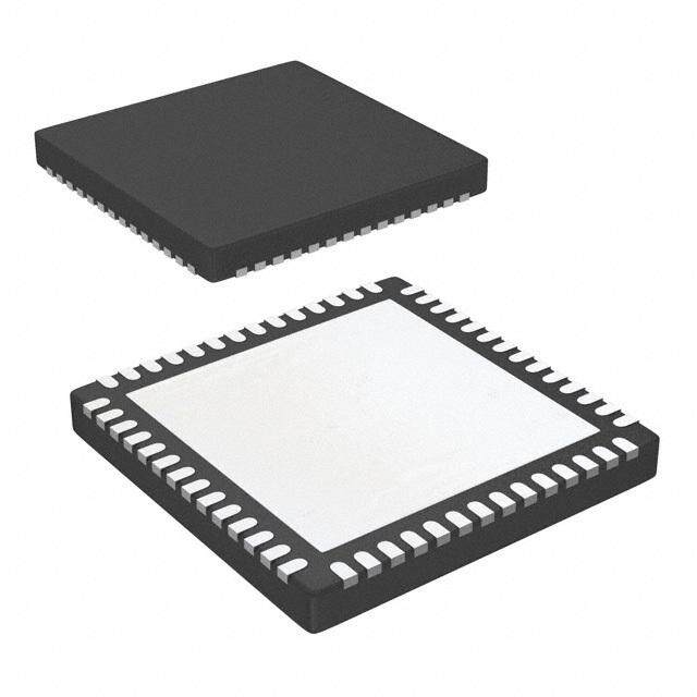
| 产品图片 |
|
| rohs | 符合RoHS无铅 / 符合限制有害物质指令(RoHS)规范要求 |
| 产品系列 | RF集成电路,调节器/解调器,Analog Devices ADL5375-05ACPZ-R7- |
| 数据手册 | |
| P1dB | 10.4dBm |
| 产品型号 | ADL5375-05ACPZ-R7 |
| PCN其它 | |
| PCN设计/规格 | |
| RF频率 | 400MHz ~ 6GHz |
| 产品目录页面 | |
| 产品种类 | 调节器/解调器 |
| 其它名称 | ADL5375-05ACPZ-R7TR |
| 功能 | 调制器 |
| 包装 | 带卷 (TR) |
| 商标 | Analog Devices |
| 安装风格 | SMD/SMT |
| 封装 | Reel |
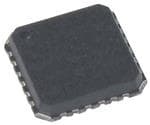
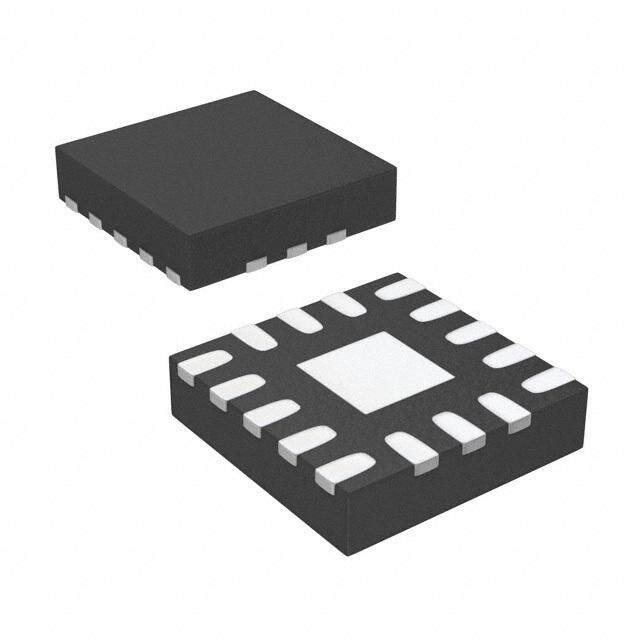
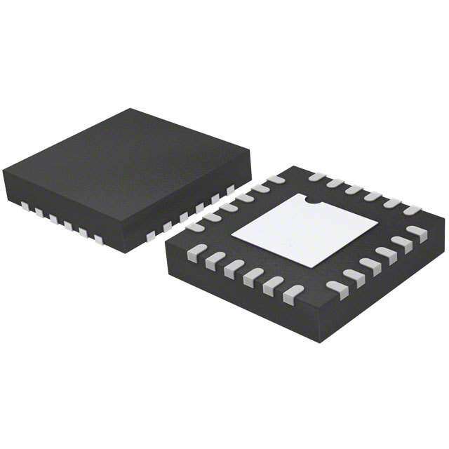
| 封装/外壳 | 24-VFQFN 裸露焊盘,CSP |
| 封装/箱体 | LFCSP-24 |
| 工作温度范围 | - 40 C to + 85 C |
| 工作电压 | 4.75 V to 5.25 V |
| 工作电流 | 174 mA |
| 工作电源电压 | 4.75 V to 5.25 V |
| 工厂包装数量 | 1500 |
| 接口类型 | LO |
| 最大功率耗散 | 1500 mW |
| 最大工作温度 | + 85 C |
| 最小工作温度 | - 40 C |
| 本底噪声 | -157.6dBm/Hz |
| 标准包装 | 1,500 |
| 测试频率 | 3.5GHz |
| 特色产品 | http://www.digikey.cn/product-highlights/zh/cn0285-direct-conversion-transmitters/50283 |
| 电压-电源 | 4.75 V ~ 5.25 V |
| 电流-电源 | 200mA |
| 电源电流 | 174 mA |
| 类型 | Modulator |
| 系列 | ADL5375 |
| 视频文件 | http://www.digikey.cn/classic/video.aspx?PlayerID=1364138032001&width=640&height=505&videoID=2245193150001http://www.digikey.cn/classic/video.aspx?PlayerID=1364138032001&width=640&height=505&videoID=2245193186001 |
| 设计资源 | |
| 调制类型 | Quadrature |
| 输出功率 | 1.71dBm |


- 商务部:美国ITC正式对集成电路等产品启动337调查
- 曝三星4nm工艺存在良率问题 高通将骁龙8 Gen1或转产台积电
- 太阳诱电将投资9.5亿元在常州建新厂生产MLCC 预计2023年完工
- 英特尔发布欧洲新工厂建设计划 深化IDM 2.0 战略
- 台积电先进制程称霸业界 有大客户加持明年业绩稳了
- 达到5530亿美元!SIA预计今年全球半导体销售额将创下新高
- 英特尔拟将自动驾驶子公司Mobileye上市 估值或超500亿美元
- 三星加码芯片和SET,合并消费电子和移动部门,撤换高东真等 CEO
- 三星电子宣布重大人事变动 还合并消费电子和移动部门
- 海关总署:前11个月进口集成电路产品价值2.52万亿元 增长14.8%


PDF Datasheet 数据手册内容提取
400 MHz to 6 GHz Broadband Quadrature Modulator Data Sheet ADL5375 FEATURES FUNCTIONAL BLOCK DIAGRAM Output frequency range: 400 MHz to 6 GHz 1 dB output compression: ≥9.4 dBm from 450 MHz to 4 GHz IBBP ADL5375 Output return loss ≤ 12 dB from 450 MHz to 4.5 GHz IBBN Noise floor: −160 dBm/Hz at 900 MHz Sideband suppression: ≤−50 dBc at 900 MHz Carrier feedthrough: ≤−40 dBm at 900 MHz LOIP QUADRATURE IQ3dB bandwidth: ≥ 750 MHz PHASE RFOUT Baseband input bias level LOIN SPLITTER DSOP ADL5375-05: 500 mV ADL5375-15: 1500 mV Single supply: 4.75 V to 5.25 V QBBN 24-lead LFCSP_VQ package QBBP 07052-001 APPLICATIONS Figure 1. Cellular communication systems GSM/EDGE, CDMA2000, W-CDMA, TD-SCDMA WiMAX/LTE broadband wireless access systems Satellite modems GENERAL DESCRIPTION The ADL5375 is a broadband quadrature modulator designed for broadband digital predistortion transmitters, and multiband operation from 400 MHz to 6 GHz. Its excellent phase accuracy radio designs. and amplitude balance enable high performance intermediate The ADL5375 accepts two differential baseband inputs and frequency or direct radio frequency modulation for commu- a single-ended LO. It generates a single-ended 50 Ω output. nication systems. The two versions offer input baseband bias levels of 500 mV The ADL5375 features a broad baseband bandwidth, along (ADL5375-05) and 1500 mV (ADL5375-15). with an output gain flatness that varies no more than 1 dB The ADL5375 is fabricated using an advanced silicon-germanium from 450 MHz to 3.5 GHz. These features, coupled with a broad- bipolar process. It is available in a 24-lead, exposed paddle, lead- band output return loss of ≤−12 dB, make the ADL5375 ideally free, LFCSP_VQ package. Performance is specified over a −40°C suited for broadband zero IF or low IF-to-RF applications, to +85°C temperature range. A lead-free evaluation board is also available. Rev. D Document Feedback Information furnished by Analog Devices is believed to be accurate and reliable. However, no responsibility is assumed by Analog Devices for its use, nor for any infringements of patents or other One Technology Way, P.O. Box 9106, Norwood, MA 02062-9106, U.S.A. rights of third parties that may result from its use. Specifications subject to change without notice. No license is granted by implication or otherwise under any patent or patent rights of Analog Devices. Tel: 781.329.4700 ©2007–2014 Analog Devices, Inc. All rights reserved. Trademarks and registered trademarks are the property of their respective owners. Technical Support www.analog.com
ADL5375 Data Sheet TABLE OF CONTENTS Features .............................................................................................. 1 LO Input ...................................................................................... 20 Applications ....................................................................................... 1 RF Output .................................................................................... 20 Functional Block Diagram .............................................................. 1 Output Disable ............................................................................ 21 General Description ......................................................................... 1 Applications Information .............................................................. 22 Revision History ............................................................................... 2 Carrier Feedthrough Nulling .................................................... 22 Specifications ..................................................................................... 3 Sideband Suppression Optimization ....................................... 22 Absolute Maximum Ratings ............................................................ 7 Interfacing the ADF4350 PLL to the ADL5375 ..................... 23 ESD Caution .................................................................................. 7 DAC Modulator Interfacing ..................................................... 24 Pin Configuration and Function Descriptions ............................. 8 GSM/EDGE Operation ............................................................. 27 Typical Performance Characteristics ............................................. 9 W-CDMA Operation ................................................................. 28 ADL5375-05 .................................................................................. 9 LO Generation Using PLLs ....................................................... 29 ADL5375-15 ................................................................................ 14 Transmit DAC Options ............................................................. 29 Theory of Operation ...................................................................... 19 Modulator/Demodulator Options ........................................... 29 Circuit Description..................................................................... 19 Evaluation Board ............................................................................ 30 Basic Connections .......................................................................... 20 Characterization Setup .................................................................. 33 Power Supply and Grounding ................................................... 20 Outline Dimensions ....................................................................... 35 Baseband Inputs .......................................................................... 20 Ordering Guide .......................................................................... 35 REVISION HISTORY 6/14—Rev. C to Rev. D Changes to Application Information Section ............................ 22 Changes to Evaluation Board Section.......................................... 30 Changes to Figure 2 .......................................................................... 8 Changes to Figure 80 ...................................................................... 34 Changes to Figure 13, Figure 14, and Figure 15 ......................... 10 Added Exposed Pad Notation to Outline Dimensions ............. 35 Changes to Figure 38, Figure 39, and Figure 40 ......................... 15 Changes to Table 9 .......................................................................... 31 11/08—Rev. 0 to Rev. A Changes to Ordering Guide .......................................................... 35 Change AD9779 to AD9779A .......................................... Universal 7/13—Rev. B to Rev. C Added Endnote, I/Q Input Bias Level and Absolute Voltage Level Parameters, Table 1 ................................................... 6 Changed CP-24-3 to CP-24-7 ........................................... Universal Added Absolute Voltage Level Parameter, Table 1 ........................ 6 9/11—Rev. A to Rev. B 12/07—Revision 0: Initial Version Changes to Features Section............................................................ 1 Replaced Table 1 ............................................................................... 3 Changes to Typical Performance Characteristics Section ........... 9 Updated Output Disable Section .................................................. 21 Rev. D | Page 2 of 36
Data Sheet ADL5375 SPECIFICATIONS V = 5 V; T = 25°C; LO = 0 dBm single-ended drive; baseband I/Q amplitude = 1 V p-p differential sine waves in quadrature with a S A 500 mV (ADL5375-05) or 1500 mV (ADL5375-15) dc bias; baseband I/Q frequency (f ) = 1 MHz, unless otherwise noted. BB Table 1. ADL5375-05 ADL5375-15 Parameter Conditions Min Typ Max Min Typ Max Unit OPERATING FREQUENCY RANGE Low frequency 400 400 MHz High frequency 6000 6000 MHz LO = 450 MHz Output Power, P V = 1 V p-p differential 0.85 0.47 dBm OUT IQ Modulator Voltage Gain RF output divided by baseband input voltage −3.1 −3.5 dB Output P1dB 9.6 10 dBm Output Return Loss −16.4 −15.2 dB Carrier Feedthrough −47.5 -42.5 dBm Sideband Suppression −37.6 −38 dBc Quadrature Error 1.7 1.49 Degrees I/Q Amplitude Balance 0.07 0.10 dB Second Harmonic P − (f + (2 × f )) −75.9 −81.5 dBc OUT LO BB ADL5375-05 P =0.85 dBm OUT ADL5375-15 P = 0.47 dBm OUT Third Harmonic P − (f + (3 × f )) −51.5 −81.6 dBc OUT LO BB ADL5375-05 P = 0.85 dBm OUT ADL5375-15 P = 0.47 dBm OUT Output IP2 f1BB = 3.5 MHz, f2BB = 4.5 MHz, baseband I/Q 65.4 64.7 dBm amplitude per tone = 0.5 V p-p differential Output IP3 f1BB = 3.5 MHz, f2BB = 4.5 MHz, baseband I/Q 26.6 23.6 dBm amplitude per tone = 0.5 V p-p differential Noise Floor I/Q inputs = 0 V differential with a dc bias −160.5 −157.0 dBm/Hz only, 20 MHz carrier offset LO = 900 MHz Output Power, P V = 1 V p-p differential 0.75 0.41 dBm OUT IQ Modulator Voltage Gain RF output divided by baseband input voltage −3.2 −3.5 dB Output P1dB 9.6 10 dBm Output Return Loss −15.7 −14.7 dB Carrier Feedthrough −45.1 −39.9 dBm Sideband Suppression −52.8 −49.9 dBc Quadrature Error 0.01 0.20 Degrees I/Q Amplitude Balance 0.07 0.10 dB Second Harmonic P − (f + (2 × f )) −75.8 −77.2 dBc OUT LO BB ADL5375-05 P = 0.75 dBm OUT ADL5375-15 P = 0.41 dBm OUT Third Harmonic P − (f + (3 × f )) −50.7 −72.7 dBc OUT LO BB ADL5375-05 P = 0.75 dBm OUT ADL5375-15 P = 0.41 dBm OUT Output IP2 f1BB = 3.5 MHz, f2BB = 4.5 MHz, baseband I/Q 62.6 64.5 dBm amplitude per tone = 0.5 V p-p differential Output IP3 f1BB = 3.5 MHz, f2BB = 4.5 MHz, baseband I/Q 25.9 23.4 dBm amplitude per tone = 0.5 V p-p differential Noise Floor I/Q inputs = 0 V differential with a dc bias −160.0 −157.1 dBm/Hz only, 20 MHz carrier offset Rev. D | Page 3 of 36
ADL5375 Data Sheet ADL5375-05 ADL5375-15 Parameter Conditions Min Typ Max Min Typ Max Unit LO = 1900 MHz Output Power, P V = 1 V p-p differential 0.53 0.49 dBm OUT IQ Modulator Voltage Gain RF output divided by baseband input voltage −3.4 −3.4 dB Output P1dB 9.9 10.5 dBm Output Return Loss −16.2 −15.5 dB Carrier Feedthrough −40.3 −35.5 dBm Sideband Suppression −50.2 −49.4 dBc Quadrature Error 0.02 0.21 Degrees I/Q Amplitude Balance 0.07 0.10 dB Second Harmonic P − (f + (2 × f )) −67.9 −72.1 dBc OUT LO BB ADL5375-05 P = 0.53dBm OUT ADL5375-15 P = 0.49dBm OUT Third Harmonic P − (f + (3 × f )) −51.8 −62.8 dBc OUT LO BB ADL5375-05 P = 0.53dBm OUT ADL5375-15 P = 0.49dBm OUT Output IP2 f1BB = 3.5 MHz, f2BB = 4.5 MHz, baseband I/Q 62.6 61 dBm amplitude per tone = 0.5 V p-p differential Output IP3 f1BB = 3.5 MHz, f2BB = 4.5 MHz, baseband I/Q 24.3 22.1 dBm amplitude per tone = 0.5 V p-p differential Noise Floor I/Q inputs = 0 V differential with a dc bias −160.0 −158.2 dBm/Hz only, 20 MHz carrier offset LO = 2150 MHz Output Power, P V = 1 V p-p differential 0.73 0.57 dBm OUT IQ Modulator Voltage Gain RF output divided by baseband input voltage −3.2 −3.4 dB Output P1dB 10.0 10.6 dBm Output Return Loss −17.1 −16.1 dB Carrier Feedthrough −39.7 −34.2 dBm Sideband Suppression −47.3 −50.2 dBc Quadrature Error −0.16 −0.18 Degrees I/Q Amplitude Balance 0.07 0.10 dB Second Harmonic P − (f + (2 × f )) −71.3 −81.7 dBc OUT LO BB ADL5375-05 P = 0.73 dBm OUT ADL5375-15 P = 0.57 dBm OUT Third Harmonic P − (f + (3 × f )) −52.4 −65.3 dBc OUT LO BB ADL5375-05 P = 0.73 dBm OUT ADL5375-15 P = 0.57 dBm OUT Output IP2 f1BB = 3.5 MHz, f2BB = 4.5 MHz, baseband I/Q 61.6 61.8 dBm amplitude per tone = 0.5 V p-p differential Output IP3 f1BB = 3.5 MHz, f2BB = 4.5 MHz, baseband I/Q 24.2 22.3 dBm amplitude per tone = 0.5 V p-p differential Noise Floor I/Q inputs = 0 V differential with a dc bias −159.5 −157.9 dBm/Hz only, 20 MHz carrier offset LO = 2600 MHz Output Power, P V = 1 V p-p differential 0.61 0.62 dBm OUT IQ Modulator Voltage Gain RF output divided by baseband input voltage −3.4 −3.3 dB Output P1dB 9.6 10.6 dBm Output Return Loss −19.3 −18 dB Carrier Feedthrough −36.5 −33.3 dBm Sideband Suppression −48.3 −48.5 dBc Quadrature Error −0.37 0.19 Degrees I/Q Amplitude Balance 0.07 0.11 dB Second Harmonic P − (f + (2 × f )) −60.9 −55.9 dBc OUT LO BB Rev. D | Page 4 of 36
Data Sheet ADL5375 ADL5375-05 ADL5375-15 Parameter Conditions Min Typ Max Min Typ Max Unit ADL5375-05 P = 0.61 dBm OUT ADL5375-15 P = 0.62 dBm OUT Third Harmonic P − (f + (3 × f )) −51.3 −57.6 dBc OUT LO BB ADL5375-05 P = 0.61 dBm OUT ADL5375-15 P = 0.62 dBm OUT Output IP2 f1BB = 3.5 MHz, f2BB = 4.5 MHz, baseband I/Q 55.0 50.1 dBm amplitude per tone = 0.5 V p-p differential Output IP3 f1BB = 3.5 MHz, f2BB = 4.5 MHz, baseband I/Q 22.7 20.7 dBm amplitude per tone = 0.5 V p-p differential Noise Floor I/Q inputs = 0 V differential with a dc bias −159.0 −157.6 dBm/Hz only, 20 MHz carrier offset LO = 3500 MHz Output Power, P V = 1 V p-p differential 0.21 0.87 dBm OUT IQ Modulator Voltage Gain RF output divided by baseband input voltage −3.8 −3.1 dB Output P1dB 9.6 10.2 dBm Output Return Loss −20.7 −19.4 dB Carrier Feedthrough −30.4 −28.6 dBm Sideband Suppression −48.3 −48.8 dBc Quadrature Error 0.01 0.13 Degrees I/Q Amplitude Balance 0.08 0.11 dB Second Harmonic P − (f + (2 × f )) −55.8 −63 dBc OUT LO BB ADL5375-05 P = 0.21 dBm OUT ADL5375-15 P = 0.87 dBm OUT Third Harmonic P − (f + (3 × f )) −50.2 −56.2 dBc OUT LO BB ADL5375-05 P = 0.21 dBm OUT ADL5375-15 P = 0.87 dBm OUT Output IP2 f1BB = 3.5 MHz, f2BB = 4.5 MHz, baseband I/Q 51.1 57.9 dBm amplitude per tone = 0.5 V p-p differential Output IP3 f1BB = 3.5 MHz, f2BB = 4.5 MHz, baseband I/Q 23.1 20.2 dBm amplitude per tone = 0.5 V p-p differential Noise Floor I/Q inputs = 0 V differential with a dc bias −157.6 −156.3 dBm/Hz only, 20 MHz carrier offset LO = 5800 MHz Output Power, P V = 1 V p-p differential −1.36 0.16 dBm OUT IQ Modulator Voltage Gain RF output divided by baseband input voltage −5.3 −3.8 dB Output P1dB 4.9 4.4 dBm Output Return Loss −7.4 −8.6 dB Carrier Feedthrough −19.5 −16.7 dBm Sideband Suppression −38.2 −39 dBc Quadrature Error −0.51 −0.50 Degrees I/Q Amplitude Balance −0.05 −0.70 dB Second Harmonic P − (f + (2 × f )) −52.6 −50 dBc OUT LO BB ADL5375-05 P = -1.36 dBm OUT ADL5375-15 P = 0.16 dBm OUT Third Harmonic P − (f + (3 × f )) −45.7 −48.4 dBc OUT LO BB ADL5375-05 P = -1.36 dBm OUT ADL5375-15 P = 0.16 dBm OUT Output IP2 f1BB = 3.5 MHz, f2BB = 4.5 MHz, baseband I/Q 39.1 38.7 dBm amplitude per tone = 0.5 V p-p differential Output IP3 f1BB = 3.5 MHz, f2BB = 4.5 MHz, baseband I/Q 14.6 11.2 dBm amplitude per tone = 0.5 V p-p differential Noise Floor I/Q inputs = 0 V differential with a dc bias −153.0 −153.4 dBm/Hz only, 20 MHz carrier offset Rev. D | Page 5 of 36
ADL5375 Data Sheet ADL5375-05 ADL5375-15 Parameter Conditions Min Typ Max Min Typ Max Unit LO INPUTS LO Drive Level Characterization performed at typical level −6 0 +6 −6 0 +6 dBm Input Return Loss 500 MHz < f < 3.3 GHz ≤−10 ≤−10 dB LO See Figure 7 and Figure 32 for return loss vs. frequency BASEBAND INPUTS Pin IBBP, Pin IBBN, Pin QBBP, Pin QBBN I/Q Input Bias Level1 500 1500 mV Absolute Voltage Level1 On Pin IBBP, Pin IBBN, Pin QBBP, Pin QBBN 0 1 1 2 V Input Bias Current Current sourcing from each baseband input 41 32 µA Input Offset Current 0.1 0.1 µA Differential Input 60 100 kΩ Impedance Bandwidth (0.1 dB) LO = 1900 MHz, baseband input = 95 80 MHz 500 mV p-p sine wave OUTPUT DISABLE Pin DSOP Off Isolation P (DSOP low) − P (DSOP high) 84 85 dB OUT OUT DSOP high, LO leakage, LO = 2150 MHz −55 −53 dBm Turn-On Settling Time DSOP high to low (90% of envelope) 220 220 ns Turn-Off Settling Time DSOP low to high (10% of envelope) 100 100 ns DSOP High Level (Logic 1) 2.0 2.0 V DSOP Low Level (Logic 0) 0.8 0.8 V POWER SUPPLIES Pin VPS1 and Pin VPS2 Voltage 4.75 5.25 4.75 5.25 V Supply Current DSOP = low 194 203 mA DSOP = high 126 127 mA 1 The input bias level can vary as long as the voltages on the individual IBBP, IBBN, QBBP, and QBBN pins remain within the specified absolute voltage level. Rev. D | Page 6 of 36
Data Sheet ADL5375 ABSOLUTE MAXIMUM RATINGS Stresses above those listed under Absolute Maximum Ratings Table 2. may cause permanent damage to the device. This is a stress Parameter Rating rating only; functional operation of the device at these or any Supply Voltage, VPOS 5.5 V other conditions above those indicated in the operational IBBP, IBBN, QBBP, QBBN 0 V to 2 V section of this specification is not implied. Exposure to absolute LOIP and LOIN 13 dBm maximum rating conditions for extended periods may affect Internal Power Dissipation device reliability. ADL5375-05 1500 mW ADL5375-15 1200 mW ESD CAUTION θ (Exposed Paddle Soldered Down)1 54°C/W JA Maximum Junction Temperature 150°C Operating Temperature Range −40°C to +85°C Storage Temperature Range −65°C to +150°C 1 Per JDEC standard JESD 51-2. For information on optimizing thermal impedance, see the Thermal Grounding and Evaluation Board Layout section. Rev. D | Page 7 of 36
ADL5375 Data Sheet PIN CONFIGURATION AND FUNCTION DESCRIPTIONS M MM VPS2COMIBBNIBBPCOMCOM 432109 222221 DSOP1 ADL5375 18VPS1 COMM2 17COMM LOIP3 TOP VIEW 16RFOUT LOIN4 (Not to Scale) 15NC COMM5 EXPOSED PAD 14COMM NC6 13NC 789012 111 CMNPMM NMBBMM COQBQBCOCO NOTES 12..NCVICOA N =AN N ELOCO TCW OE IXNMPNPOEECSDTEA.DN D CPOEA NDPO ATTTO HC T.OHNEN GERCOT UTNOD T LHAISN EPIN. 07052-003 Figure 2. Pin Configuration Table 3. Pin Function Descriptions Pin No. Mnemonic Description 1 DSOP Output Disable. A logic high on this pin disables the RF output. Connect this pin to ground or leave it floating to enable the output. 2, 5, 8, 11, 12, COMM Input Common Pins. Connect to the ground plane via a low impedance path. 14, 17, 19, 20, 23 3, 4 LOIP, LOIN Local Oscillator Inputs. Single-ended operation: The LOIP pin is driven from the LO source through an ac-coupling capacitor while the LOIN pin is ac-coupled to ground through a capacitor. Differential operation: The LOIP and LOIN pins must be driven differentially through ac-coupling capacitors in this mode of operation. 6, 7, 13, 15, NC No Connect. These pins can be left open or tied to ground. 9, 10, 21, 22 QBBN, QBBP, Differential In-Phase and Quadrature Baseband Inputs. These high impedance inputs should be dc- IBBP, IBBN biased to the recommended level depending on the version. ADL5375-05: 500 mV ADL5375-15: 1500 mV These inputs should be driven from a low impedance source. Nominal characterized ac signal swing is 500 mV p-p on each pin. This results in a differential drive of 1 V p-p. These inputs are not self-biased and have to be externally biased. 16 RFOUT RF Output. Single-ended, 50 Ω internally biased RF output. RFOUT must be ac-coupled to the load. 18, 24 VPS1, VPS2 Positive Supply Voltage Pins. All pins should be connected to the same supply (V). To ensure adequate S external bypassing, connect 0.1 µF and 100 pF capacitors between each pin and ground. EP Exposed Paddle. Connect to the ground plane via a low impedance path. Rev. D | Page 8 of 36
Data Sheet ADL5375 TYPICAL PERFORMANCE CHARACTERISTICS ADL5375-05 V = 5 V; T = 25°C; LO = 0 dBm single-ended drive; baseband I/Q amplitude = 1 V p-p differential sine waves in quadrature with a S A 500 mV dc bias; baseband I/Q frequency (f ) = 1 MHz, unless otherwise noted. BB 5 12 4 VS = 5.25V m) 10 VS = 5.0V 3 B R (dBm) 2 TA = –40°C TA = +25°C SION (d 8 VS = 4.75V OWE 1 PRES T P 0 OM 6 U C B OUTP ––21 TA = +85°C UTPUT 4 S O S –3 B 1d 2 –4 –50 0.5 1.0 1.5 2L.O0 F2R.E5QU3E.0NC3Y. 5(GH4z.)0 4.5 5.0 5.5 6.0 07052-052 00 0.5 1.0 1.5 2L.O0 F2R.E5QU3E.0NC3Y. 5(GH4z.)0 4.5 5.0 5.5 6.0 07052-055 Figure 3. Single-Sideband (SSB) Output Power (POUT) vs. Figure 6. SSB Output 1dB Compression Point (OP1dB) vs. LO Frequency (fLO) LO Frequency (fLO) and Temperature and Supply 90 5 120 60 4 3 m) dB 2 150 30 1 42050.7M3H –z j8.14Ω WER ( 1 VS = 5.25V 400MHz 3 2 S6G11Hz O 75.88 – j76.94Ω T P 0 180 1 0 3 S22 TPU –1 VS = 5.0V 400MHz 44000.0M1H +z j9.20Ω OU VS = 4.75V 4 2 4 S22 SSB –2 210 6GHz 6GHz 330 63G0.H52z – j30.09Ω –3 –4 S11 240 S22 300 –50 0.5 1.0 1.5 2L.O0 F2R.E5QU3E.0NC3Y. 5(GH4z.)0 4.5 5.0 5.5 6.0 07052-053 270 07052-097 Figure 7. Smith Chart of LOIP (LOIN AC-Coupled to Ground) S11 and RFOUT Figure 4. Single-Sideband (SSB) Output Power (POUT) vs. S22 from 450 MHz to 6000 MHz LO Frequency (fLO) and Supply 14 0 LOIP m) 12 B –5 d N ( 10 TA = –40°C O SI B) –10 S d PRE 8 TA = +85°C TA = +25°C SS ( M O UTPUT CO 46 RETURN L ––2105 RFOUT O B d 1 2 –25 00 0.5 1.0 1.5 2L.O0 F2R.E5QU3E.0NC3Y. 5(GH4z.)0 4.5 5.0 5.5 6.0 07052-054 –300 0.5 1.0 1.5 2.0FRE2Q.5UE3N.0CY 3(G.5Hz)4.0 4.5 5.0 5.5 6.0 07052-056 Figure 5. SSB Output 1dB Compression Point (OP1dB) vs. LO Frequency (fLO) Figure 8. Return Loss of LOIP (LOIN AC-Coupled to Ground) S11 and RFOUT and Temperature S22 from 450 MHz to 6000 MHz Rev. D | Page 9 of 36
ADL5375 Data Sheet 0 0 –5 –10 –10 GH (dBm) ––2105 TA = +85°C TA = +25°C ON (dBc) –20 OU –25 SSI –30 TA = +25°C R E H R EEDT ––3350 TA = –40°C SUPP –40 TA = +85°C ER F –40 AND –50 CARRI ––5405 SIDEB –60 –70 –55 TA = –40°C –600 0.5 1.0 1.5 2L.O0 F2R.E5QU3E.0NC3Y. 5(GH4z.)0 4.5 5.0 5.5 6.0 07052-057 –800 0.5 1.0 1.5 2L.O0 F2R.E5QU3E.0NC3Y. 5(GH4z.)0 4.5 5.0 5.5 6.0 07052-060 Figure 9. Carrier Feedthrough vs. LO Frequency (fLO) and Temperature; Figure 12. Sideband Suppression vs. LO Frequency (fLO) and Temperature Multiple Devices Shown After Nulling at 25°C; Multiple Devices Shown 0 –10 10 R CARRIER FEEDTHROUGH (dBm) ––––––654321000000 TA = +85TT°AAC == –+4205°°CC D-ORDER DISTORTION, THIRD-ORDEORTION, CARRIER FEEDTHROUGH,AND SIDEBAND SUPPRESSION ––––––––9876543200000000 FEEDTCHARRORUIGERH (dBmPS)OSWB EORU T(dPBUmT)SUPPSRIDEESBSIAONND (dBc) ––05510 SSB OUTPUT POWER (dBm) NT –70 ECODIS –100 THIRD-ORDER DSISETCOORNTDI-OONR D(dEBRc) S DISTORTION (dBc) –800 0.5 1.0 1.5 2L.O0 F2R.E5QU3E.0NC3Y. 5(GH4z.)0 4.5 5.0 5.5 6.0 07052-058 –1100.2 BASEBAND DIFFERENTIAL 1INPUT VOLTAGE (V p-p) 4–15 07052-061 Figure 10. Carrier Feedthrough vs. LO Frequency (fLO) and Temperature Figure 13. Second- and Third-Order Distortion, Carrier Feedthrough, After Nulling at 25°C; Multiple Devices Shown Sideband Suppression, and SSB POUT vs. Baseband Differential Input Level (fLO = 900 MHz) –10 10 0 R SSB OUTPUT SIDEBAND SUPPRESSION (dBc) –––––––76543210000000 TA = +25°TCA = +T85A° =C –40°C ECOND-ORDER DISTORTION, THIRD-ORDEDISTORTION, CARRIER FEEDTHROUGH,AND SIDEBAND SUPPRESSION–1––––––––098765432000000000 FEEDTCHTARHROIRRUIDGE-RHO R(dDBEmR) POWERD S(IdSEBTCmOOSR)NUTDPI-OPOSNRRI DED(dESEBBSRcIAO)NND (dBc) ––05150 SSB OUTPUT POWER (dBm) S DISTORTION (dBc) –800 0.5 1.0 1.5 2L.O0 F2R.E5QU3E.0NC3Y. 5(GH4z.)0 4.5 5.0 5.5 6.0 07052-059 –1100.2 BASEBAND DIFFERENTIAL 1INPUT VOLTAGE (V p-p) 4–15 07052-062 Figure 14. Second- and Third-Order Distortion, Carrier Feedthrough, Figure 11. Sideband Suppression vs. LO Frequency (fLO) and Temperature; Multiple Devices Shown Sideband Suppression, and SSB POUT vs. Baseband Differential Input Level (fLO = 2150 MHz) Rev. D | Page 10 of 36
Data Sheet ADL5375 0 10 30 R SSB OUTPUT ECOND-ORDER DISTORTION, THIRD-ORDEDISTORTION, CARRIER FEEDTHROUGH,AND SIDEBAND SUPPRESSION –––––––––987654321000000000 DFIETSEHTDOIRTRDCHT-AROIORORNRUD I(GEEdRRHB c(d)Bm) PODWSIESERTCO O(dRNBTDmI-OSO)NUR PD(dPESBRRIcDE)ESBSIAONND (dBc) ––05150 SSB OUTPUT POWER (dBm) OUTPUT THIRD-ORDER INTERCEPT (dBm) 221150505 TA = +25°TCTAA = = + –8450°°CC S –1000.2 BASEBAND DIFFERENTIAL 1INPUT VOLTAGE (V p-p) 4–15 07052-063 00 0.5 1.0 1.5 2L.O0 F2R.E5QU3E.0NC3Y. 5(GH4z.)0 4.5 5.0 5.5 6.0 07052-087 Figure 15. Second- and Third-Order Distortion, Carrier Feedthrough, Figure 18. OIP3 vs. LO Frequency (fLO) and Temperature (POUT ≈ −5 dBm) Sideband Suppression, and SSB POUT vs. Baseband Differential Input Level (fLO = 3500 MHz) –10 80 m) RDER DISTORTION ANDDER DISTORTION (dBc)––––54320000 THIRD-ORDER TA = –40°C TA = +85°C ND-ORDER INTERCEPT (dB 3456700000 TA = +25°C TA = –40°C SECOND-OTHIRD-OR––7600 SECOND-ORDER TA = +25°C TPUT SECO 1200 TA = +85°C U O –800 0.5 1.0 1.5 2L.O0 F2R.E5QU3E.0NC3Y. 5(GH4z.)0 4.5 5.0 5.5 6.0 07052-064 00 0.5 1.0 1.5 2L.O0 F2R.E5QU3E.0NC3Y. 5(GH4z.)0 4.5 5.0 5.5 6.0 07052-088 Figure 16. Second- and Third-Order Distortion vs. LO Frequency (fLO) and Figure 19. OIP2 vs. LO Frequency (fLO) and Temperature (POUT ≈ −5 dBm) Temperature (Baseband I/Q Amplitude = 1 V p-p Differential) –20 1.5 –20 2 SECOND-ORDER DISTORTION,CARRIER FEEDTHROUGH,SIDEBAND SUPPRESSION (dB)––––65430000 SUPPSRIDEESBSAIONSNDS (BdB OcU)TPUT POWERF (EdEBDDmSITES)CHCTAROORORNRUDTIIG-EOORHNR (D(ddEBBRmc)) 0–––.2105...555 SSB OUTPUT POWER (dBm) SECOND-ORDER DISTORTION, THIRD-ORDERDISTORTION,SIDEBAND SUPPRESSION (dBc),AND CARRIER FEEDTHROUGH (dBm) –––––7654300000 PSOSFWBSE EUOERPUD PT(TSdRCPHIBDEAURmESRTOBS)RUIAIOGENNRHD ((ddBBcm))DSISETCOORNTDI-OONRD D(IdTSEBHTRcOIR)RDT-OIORND (EdRBc) –––01321 SSB OUTPUT POWER (dBm) –701 BASEBAND FR1E0QUENCY (MHz) 100–3.5 07052-098 –80–6 –4 –L2O AMPLIT0UDE (dBm2) 4 6–4 07052-065 Figure 17. Second-Order Distortion, Carrier Feedthrough, Sideband Figure 20. Second- and Third-Order Distortion, Carrier Feedthrough, Suppression, and SSB POUT vs. Baseband Frequency (fBB); fLO = 2140 MHz Sideband Suppression, and SSB POUT vs. LO Amplitude (fLO = 900 MHz) Rev. D | Page 11 of 36
ADL5375 Data Sheet –20 2 SECOND-ORDER DISTORTION, THIRD-ORDERDISTORTION,SIDEBAND SUPPRESSION (dBc),AND CARRIER FEEDTHROUGH (dBm) –––––7654300000 FEEDTCHARRORUSIGEUDSRHPISE P(TCSdROIOBDERmNESTDBS)I-OIAOONNRND D( (ddEBBRcc))PSOSWB EDORIUTS T(HTdPOIBRURmDTT-)OIORND (EdRBc) –––01321 SSB OUTPUT POWER (dBm) QUANTITY 11111024682468 –80–6 –4 –L2O AMPLIT0UDE (dBm2) 4 6–4 07052-066 0–160.5 –160.3 –160.1 –N15O9I.S9E –(d1B59m.7/Hz–)159.5 –159.3 –159.1 07052-089 Figure 21. Second- and Third-Order Distortion, Carrier Feedthrough, Figure 24. 20 MHz Offset Noise Floor Distribution at fLO = 900 MHz Sideband Suppression, and SSB POUT vs. LO Amplitude (fLO = 2150 MHz) (I/Q Amplitude = 0 mV p-p with 500 mV DC Bias) –10 1 N, THIRD-ORDERPRESSION (dBc),OUGH (dBm) ––3200 FEEDTCHARRORUIGERH (dBm) PSOSWB EORU T(dPBUmT) –01 R (dBm) 678 SECOND-ORDER DISTORTIODISTORTION,SIDEBAND SUPAND CARRIER FEEDTHR –––654000 DITSHTOIRRDT-OIORND (EdRBc) SUPPSRDIDSEISEESTCBSOIOAORNNNTDD I(-OdOBNRc D()dEBRc) –––432 SSB OUTPUT POWE QUANTITY 12345 –70–6 –4 –L2O AMPLIT0UDE (dBm2) 4 6–5 07052-067 0–160.5 –160.1 –N15O9I.S7E (dBm–1/H59z.)3 –158.9 –158.5 07052-090 Figure 22. Second- and Third-Order Distortion, Carrier Feedthrough, Figure 25. 20 MHz Offset Noise Floor Distribution at fLO = 2140 MHz Sideband Suppression, and SSB POUT vs. LO Amplitude (fLO = 3500 MHz) (I/Q Amplitude = 0 mV p-p with 500 mV DC Bias) 210 10 205 VS = 5.25V 9 200 8 T (mA) 195 VS = 5.0V 7 N Y 6 PPLY CURRE 111988050 VS = 4.75V QUANTIT 45 U 3 S 175 2 170 1 165 –40 TEMPERA25TURE (°C) 85 07052-068 0–158.9 –158.5 –158N.1OIS–E1 (5d7B.7m/Hz–)157.3 –156.9 –156.5 07052-099 Figure 23. Power Supply Current vs. Temperature Figure 26. 20 MHz Offset Noise Floor Distribution at fLO = 3500 MHz (I/Q Amplitude = 0 mV p-p with 500 mV DC Bias) Rev. D | Page 12 of 36
Data Sheet ADL5375 86 0 B) 88 –10 ATION (d 85 SSB OUTPUT POWER ISOLATION (dB) –20 H (dBm) SOL 83 –30 OUG R I HR WE 82 –40 DT O E TPUT P 81 CARRIER FEEDTHROUGH (dBm) –50 RIER FE U 80 –60 R O A B C SS 79 –70 780 0.5 1.0 1.5 2L.O0 F2R.E5QU3E.0NC3Y. 5(GH4z.)0 4.5 5.0 5.5 6.0–80 07052-091 Figure 27. SSB POUT Isolation and Carrier Feedthrough with DSOP High Rev. D | Page 13 of 36
ADL5375 Data Sheet ADL5375-15 V = 5 V; T = 25°C; LO = 0 dBm single-ended drive; baseband I/Q amplitude = 1 V p-p differential sine waves in quadrature with a S A 1500 mV dc bias; baseband I/Q frequency (f ) = 1 MHz, unless otherwise noted. BB 5 12 4 VS = 5.25V m) 10 VS = 5.0V 3 B R (dBm) 2 TA = –40°C TA = +25°C SION (d 8 WE 1 ES VS = 4.75V TPUT PO –10 TA = +85°C T COMPR 6 U U O P 4 B –2 UT S O S –3 B 1d 2 –4 –50 0.5 1.0 1.5 2L.O0 F2R.E5QU3E.0NC3Y. 5(GH4z.)0 4.5 5.0 5.5 6.0 07052-069 00 0.5 1.0 1.5 2L.O0 F2R.E5QU3E.0NC3Y. 5(GH4z.)0 4.5 5.0 5.5 6.0 07052-072 Figure 28. Single-Sideband (SSB) Output Power (POUT) vs. LO Frequency (fLO) Figure 31. SSB Output 1dB Compression Point (OP1dB) vs. LO Frequency (fLO) and Temperature and Supply 90 5 120 60 4 3 m) R (dB 2 VS = 4.75V 150 400MHz 30 1 S420510.10M7H –z j7.11Ω WE 1 VS = 5.0V 3 2 S11 O 6GHz SSB OUTPUT P ––210 VS = 5.25V 182010 400MHz1 6GHz4 2 6GHz 3300 34 9S43S6608G22.0.22H96M83z H –+z jj7140..7354ΩΩ –3 34.35 – j30.63Ω –4 Figure– 5209. Si0n.5gle-1S.0ide1b.5and2L. O(0S SF2BR.)E5 OQUu3Et.0pNuCt3Y .P 5(oGwH4ze.)0r (P4O.5UT) v5.s0. LO5. 5Fre6q.u0en07052-070cy 240 SS2127120 300 07052-102 Figure 32. Smith Chart of LOIP (LOIN AC-Coupled to Ground) S11 and RFOUT (fLO) and Supply S22 from 450 MHz to 6000 MHz 12 0 TA = –40°C Bm) 10 –5 N (d TA = +25°C LOIP UTPUT COMPRESSIO 468 TA = +85°C RETURN LOSS (dB) –––211050 RFOUT O B 1d 2 –25 00 0.5 1.0 1.5 2L.O0 F2R.E5QU3E.0NC3Y. 5(GH4z.)0 4.5 5.0 5.5 6.0 07052-071 –300 0.5 1.0 1.5 2.0FRE2Q.5UE3N.0CY 3(G.5Hz)4.0 4.5 5.0 5.5 6.0 07052-073 Figure 30. SSB Output 1dB Compression Point (OP1dB) vs. LO Frequency (fLO) Figure 33. Return Loss of LOIP (LOIN AC-Coupled to Ground) S11 and RFOUT and Temperature S22 from 450 MHz to 6000 MHz Rev. D | Page 14 of 36
Data Sheet ADL5375 0 0 –5 –10 –10 m) c) GH (dB ––2105 TA = +85°C ON (dB –20 TA = +85°C U SI –30 HRO –25 TA = –40°C RES TA = –40°C DT –30 PP –40 ER FEE ––4305 TA = +25°C AND SU –50 CARRI ––5405 SIDEB –60 –70 –55 TA = +25°C –600 0.5 1.0 1.5 2L.O0 F2R.E5QU3E.0NC3Y. 5(GH4z.)0 4.5 5.0 5.5 6.0 07052-074 –800 0.5 1.0 1.5 2L.O0 F2R.E5QU3E.0NC3Y. 5(GH4z.)0 4.5 5.0 5.5 6.0 07052-077 Figure 34. Carrier Feedthrough vs. LO Frequency (fLO) and Temperature; Figure 37. Sideband Suppression vs. LO Frequency (fLO) and Temperature Multiple Devices Shown After Nulling at 25°C; Multiple Devices Shown 0 0 10 R SSB OUTPUT ARRIER FEEDTHROUGH (dBm) ––––––654321000000 TA = –T4A0 °=C +85°C TA = +25°C D-ORDER DISTORTION, THIRD-ORDEORTION, CARRIER FEEDTHROUGH,AND SIDEBAND SUPPRESSION ––––––––1432876500000000 SUPPSRIDEESFBSEIAEONDNDT C(HdARBROcR)UIGERH (dPBOmW)ER (dBm) ––05150 SSB OUTPUT POWER (dBm) C –70 ECONDIST –90 DITSHTOIRRDT-OIORND (EdRBc) DSISETCOORNTDI-OONR D(dEBRc) S –800 0.5 1.0 1.5 2L.O0 F2R.E5QU3E.0NC3Y. 5(GH4z.)0 4.5 5.0 5.5 6.0 07052-075 –1000.2 BASEBAND DIFFERENTIAL 1INPUT VOLTAGE (V p-p) 4–15 07052-078 Figure 35. Carrier Feedthrough vs. LO Frequency (fLO) and Temperature After Figure 38. Second- and Third-Order Distortion, Carrier Feedthrough, Nulling at 25°C; Multiple Devices Shown Sideband Suppression, and SSB POUT vs. Baseband Differential Input Level (fLO = 900 MHz) 0 0 10 R SSB OUTPUT ND SUPPRESSION (dBc) –––––5432100000 TA = +25°C TA = –40°C ER DISTORTION, THIRD-ORDEN, CARRIER FEEDTHROUGH,DEBAND SUPPRESSION ––––––432165000000 SUPPSRIDEESFBSEIAEONDNDT C(HdARBROcR)UIGERH (dPBOmW)ER (dBm) –055 OUTPUT POWER (dBm) SIDEBA ––7600 TA = +85°C ECOND-ORDDISTORTIOAND SI –––987000 DITSHTOIRRDT-OIORND (EdRBc) DSISETCOORNTDI-OONR D(dEBRc) –10 SSB S –800 0.5 1.0 1.5 2L.O0 F2R.E5QU3E.0NC3Y. 5(GH4z.)0 4.5 5.0 5.5 6.0 07052-076 –1000.2 BASEBAND DIFFERENTIAL 1INPUT VOLTAGE (V p-p) 4–15 07052-079 Figure 36. Sideband Suppression vs. LO Frequency (fLO) and Temperature; Figure 39. Second- and Third-Order Distortion, Carrier Feedthrough, Multiple Devices Shown Sideband Suppression, and SSB POUT vs. Baseband Differential Input Level (fLO = 2150 MHz) Rev. D | Page 15 of 36
ADL5375 Data Sheet 0 10 30 R SSB OUTPUT SECOND-ORDER DISTORTION, THIRD-ORDEDISTORTION, CARRIER FEEDTHROUGH,AND SIDEBAND SUPPRESSION –––––––––987654321000000000 FEEDTCHDARITSROHTRUOIIRGERDRHT- OI(OdRNBD m(Ed)RBc)PDOSISWETCEOORRN (TDdIB-OOmNRS) DU(dEPBRPcSR)IDEESBSIAONND (dBc) ––05150 SSB OUTPUT POWER (dBm) OUTPUT THIRD-ORDER INTERCEPT (dBm) 111112222202468024682468 TA = +25°C TTAA == –+4805°°CC –1000.2 BASEBAND DIFFERENTIAL 1INPUT VOLTAGE (V p-p) 4–15 07052-080 00 0.5 1.0 1.5 2L.O0 F2R.E5QU3E.0NC3Y. 5(GH4z.)0 4.5 5.0 5.5 6.0 07052-092 Figure 40. Second- and Third-Order Distortion, Carrier Feedthrough, Figure 43. OIP3 vs. LO Frequency (fLO) and Temperature (POUT ≈ −5 dBm at Sideband Suppression, and SSB POUT vs. Baseband Differential Input Level fLO = 900 MHz) (fLO = 3500 MHz) 0 m) 70 B d ORTION ANDRTION (dBc)–––321000 ER INTERCEPT ( 5600 TA = –40°C R DISTDISTO–40 THIRD-ORDER D-ORD 40 TA = +25°C ORDERDER –50 TA = +25°C ECON 30 TA = +85°C SECOND-THIRD-O––7600 TA = –40°C TA = +85°C OUTPUT S 1200 SECOND-ORDER –800 0.5 1.0 1.5 2L.O0 F2R.E5QU3E.0NC3Y. 5(GH4z.)0 4.5 5.0 5.5 6.0 07052-081 00 0.5 1.0 1.5 2L.O0 F2R.E5QU3E.0NC3Y. 5(GH4z.)0 4.5 5.0 5.5 6.0 07052-093 Figure 41. Second- and Third-Order Distortion vs. LO Frequency (fLO) and Figure 44. OIP2 vs. LO Frequency (fLO) and Temperature (POUT ≈ −5 dBm at Temperature (Baseband I/Q Amplitude = 1 V p-p Differential) fLO = 900 MHz) –20 2 –20 1.5 R SSB OUTPUT POWER (dBm) E SECOND-ORDER DISTORTION,CARRIER FEEDTHROUGH,SIDEBAND SUPPRESSION––––65430000 FEEDTCHARRORUIGERH (dBm) SUPPSRIDEESBSAIONND (dBc) 0–––.2105...555 SSB OUTPUT POWER (dBm) ND-ORDER DISTORTION, THIRD-ORDTORTION, CARRIER FEEDTHROUGH,ND SIDEBAND SUPPRESSION (dBc) –––––7654300000 FEEDTCHSARUROPRUPISGERIRHDE ES(dBSBIAOmNN)D (dBPScOS)WB EORUD T(dIPTSBUHTmOTIR)RDT-OIORND (EdRBc) –011 SSB OUTPUT POWER (dBm) SECOND-ORDER ECODISA –80 SECOND-ORDER DISTORTION(dBc) S DISTORTION (dBc) –701 BASEBAND FR1E0QUENCY (MHz) 100–3.5 07052-103 –90–6 –4 –L2O AMPLIT0UDE (dBm2) 4 6–2 07052-082 Figure 42. Second-Order Distortion, Carrier Feedthrough, Sideband Figure 45. Second- and Third-Order Distortion, Carrier Feedthrough, Suppression, and SSB POUT vs. Baseband Frequency (fBB); fLO = 2140 MHz Sideband Suppression, and SSB POUT vs. LO Amplitude (fLO = 900 MHz) Rev. D | Page 16 of 36
Data Sheet ADL5375 –20 2 18 R CARRIER ER DISTORTION, THIRD-ORDEN, CARRIER FEEDTHROUGH,BAND SUPPRESSION (dBc) ––––65430000 SFUEPEPDSRTIDEHESRBSOIAUONGNDH (d (BdDBcI)mTSHT)OIRRDT-OIOPSRONSD WB(Ed EROBRUc )T(dPBUmT) 01 OUTPUT POWER (dBm) QUANTITY 1111024668 D-ORDORTIOD SIDE –1 SSB 4 CONDISTAN –70 SECOND-ORDER 2 E DISTORTION (dBc) S –80–6 –4 –L2O AMPLIT0UDE (dBm2) 4 6–2 07052-083 0–158.0 –157.8 –157.6 –N15O7I.S4E –(d1B57m.2/Hz–)157.0 –156.8 –156.6 07052-094 Figure 46. Second- and Third-Order Distortion, Carrier Feedthrough, Figure 49. 20 MHz Offset Noise Floor Distribution at fLO = 900 MHz (I/Q Amplitude = 0 mV p-p with 1500 mV DC Bias) Sideband Suppression, and SSB POUT vs. LO Amplitude (fLO = 2150 MHz) –20 2.0 12 R CARRIER E FEEDTHROUGH (dBm) ORDUGH,Bc) –30 SSB OUTPUT 1.5 10 ER DISTORTION, THIRD-N, CARRIER FEEDTHROBAND SUPPRESSION (d –––654000 POWER (dBm) SUPPSRIDEESBSIAONND (dBc) –0010..50.5 OUTPUT POWER (dBm) QUANTITY 468 D-ORDORTIOD SIDE DITSHTOIRRDT-OIORND (EdRBc) DSISETCOORNTDI-OONR D(dEBRc) –1.0 SSB CONDISTAN –70 –1.5 2 E S –80–6 –4 –L2O AMPLIT0UDE (dBm2) 4 6–2.0 07052-084 0–158.5 –158.3 –158.1 –N15O7I.S9E –(d1B57m.7/Hz–)157.5 –157.3 –157.1 07052-095 Figure 47. Second- and Third-Order Distortion, Carrier Feedthrough, Figure 50. 20 MHz Offset Noise Floor Distribution at fLO = 2140 MHz Sideband Suppression, and SSB POUT vs. LO Amplitude (fLO = 3500 MHz) (I/Q Amplitude = 0 mV p-p with 1500 mV DC Bias) 0.230 9 8 0.220 VS = 5.25V 7 A) 0.210 T ( VS = 5.0V 6 N URRE 0.200 VS = 4.75V NTITY 5 C A Y 0.190 U 4 L Q P UP 3 S 0.180 2 0.170 1 0.160 –40 TEMPERA25TURE (°C) 85 07052-085 0–157.5 –157.1 –N1O56IS.7E (dBm–1/H56z.)3 –155.9 –155.5 07052-104 Figure 48. Power Supply Current vs. Temperature Figure 51. 20 MHz Offset Noise Floor Distribution at fLO = 3500 MHz (I/Q Amplitude = 0 mV p-p with 500 mV DC Bias) Rev. D | Page 17 of 36
ADL5375 Data Sheet 88 0 LATION (dB) 8846 SSB OUTPUT POWER ISOLATION (dB) –––321000 GH (dBm) SO OU R I 82 –40 HR WE DT UTPUT PO 7880 CARRIER FEEDTHROUGH (dBm) ––6500 RRIER FEE O –70 A B C SS 76 –80 740 0.5 1.0 1.5 2L.O0 F2R.E5QU3E.0NC3Y. 5(GH4z.)0 4.5 5.0 5.5 6.0–90 07052-096 Figure 52. SSB POUT Isolation and Carrier Feedthrough with DSOP High Rev. D | Page 18 of 36
Data Sheet ADL5375 THEORY OF OPERATION CIRCUIT DESCRIPTION V-to-I Converter The ADL5375 can be divided into five circuit blocks: the LO The differential baseband inputs (QBBP, QBBN, IBBN, and interface, the baseband voltage-to-current (V-to-I) converter, IBBP) present a high impedance. The voltages applied to these the mixers, the differential-to-single-ended (D-to-S) stage, pins drive the V-to-I stage that converts baseband voltages into and the bias circuit. A block diagram of the device is shown in currents. The differential output currents of the V-to-I stages Figure 53. feed each of their respective mixers. The dc common-mode voltage at the baseband inputs sets the currents in the two LOIP PHASE mixer cores. Varying the baseband common-mode voltage LOIN SPLITTER influences the current in the mixer and affects overall modula- tor performance. The recommended dc voltage for the baseband common-mode voltage is 500 mV dc for the ADL5375-05 and 1500 mV for the ADL5375-15. IBBP IBBN Mixers Σ RFOUT The ADL5375 has two double-balanced mixers: one for the QQBBBBNP DSOP 07052-028 inne-lp (hQa-sceh cahnannenl)e.l T(Ih ceh oauntnpeult) caunrdr eonntes ffroorm th teh qeu tawdor amtuixree rcsh saunm- Figure 53. Block Diagram together into an internal load. The signal developed across this The LO interface generates two LO signals in quadrature. load is used to drive the D-to-S stage. These signals are used to drive the mixers. The I/Q baseband D-to-S Stage input signals are converted to currents by the V-to-I stages, The output D-to-S stage consists of an on-chip active balun which then drive the two mixers. The outputs of these mixers that converts the differential signal to a single-ended signal. combine to feed the output balun, which provides a single- The balun presents 50 Ω impedance to the output (VOUT). ended output. The bias cell generates reference currents for Therefore, no matching network is needed at the RF output the V-to-I stage. for optimal power transfer in a 50 Ω environment. LO Interface Bias Circuit The LO interface consists of a polyphase quadrature splitter An on-chip band gap reference circuit is used to generate a and a limiting amplifier. The LO input impedance is set by proportional-to-absolute temperature (PTAT) reference current the polyphase splitter. Each quadrature LO signal then passes for the V-to-I stage. through a limiting amplifier that provides the mixer with a DSOP limited drive signal. The DSOP pin can be used to disable the output stage of the The LO input can be driven single-ended or differentially. modulator. If the DSOP pin is connected to ground or left For applications above 3 GHz, improved OIP2 and LO leakage unconnected, the part operates normally. If the DSOP pin is may result from driving the LO input differentially. connected to the positive voltage supply, the output stage is disabled and the LO leakage is also reduced. Rev. D | Page 19 of 36
ADL5375 Data Sheet BASIC CONNECTIONS IBBN IBBP VPOS C5 C3 M M M VPOS 0.1µF 100pF VPS2 COM IBBN IBBP COM COM 4 3 2 1 0 9 S1 2 2 2 2 2 1 A B VPOS C2 C4 DSOP VPS1 100pF 0.1µF 1 18 C6 COMM COMM 100pF 2 Z1 17 LOIP LOIP 3 ADL5375 16 RFOUT RFOUT LOIN 4 15 NC C1 C7 COMM COMM 100pF 100pF 5 14 EXPOSED PADDLE NC 6 13 NC 7 8 9 10 11 12 CM N P M M NM B B M M O B B O O C Q Q C C GND QBBN QBBP 07052-029 Figure 54. Basic Connections for the ADL5375 Figure 54 shows the basic connections for the ADL5375. All the baseband inputs must be externally dc biased. The recommended common-mode level is dependent on the POWER SUPPLY AND GROUNDING version of the ADL5375. Pin VPS1 and Pin VPS2 should be connected to the same 5 V ADL5375-05: 500 mV source. Each pin should be decoupled with a 100 pF and 0.1 μF capacitor. These capacitors should be located as close ADL5375-15: 1500 mV as possible to the device. The power supply can range between LO INPUT 4.75 V and 5.25 V. The LO input is designed to be driven from a single-ended The ten COMM pins should be tied to the same ground plane source. The LO source is ac-coupled through a series capacitor through low impedance paths. to the LOIP pin while the LOIN pin is ac-coupled to ground The exposed paddle on the underside of the package should through a second capacitor. also be soldered to a ground plane with low thermal and The typical LO drive level, which was used for the characterization electrical impedance. If the ground plane spans multiple layers of the ADL5375, is 0 dBm. on the circuit board, they should be stitched together with nine vias under the exposed paddle as illustrated in the Evaluation Differential operation is also possible, in which case both sides Board section. The AN-772 Application Note discusses the of the differential LO source should be ac-coupled through a thermal and electrical grounding of the LFCSP (QFN) package pair of series capacitors to the LOIP and LOIN pins. in detail. RF OUTPUT BASEBAND INPUTS The RF output is available at the RFOUT pin (Pin 16), which can The baseband inputs (IBBP, IBBN, QBBP, and QBBN) should be drive a 50 Ω load. The internal balun provides a low dc path to driven from a differential source. The nominal drive level used ground. In most situations, the RFOUT pin must be ac-coupled in the characterization of the ADL5375 is 1 V p-p differential to the load. (or 500 mV p-p on each pin). Rev. D | Page 20 of 36
Data Sheet ADL5375 OUTPUT DISABLE to just above the KT thermal noise level. Asserting DSOP also reduces the supply current of the ADL5375 from 200 mA to The ADL5375 incorporates an output disable pin feature that 127 mA. shuts down the output amplifier stage to isolate the modulator from the load. This output is disabled when the voltage on the The time delay between when DSOP pin going low and the DSOP exceeds 2 V. The output is enabled when the DSOP pin is output power being restored is approximately 200 ns. The time either tied to ground or left unconnected. delay when DSOP going high and output being disabled is less than 100 ns. Asserting DSOP further reduces LO leakage (see Figure 27 and Figure 52) and drives the broadband noise of the device down Rev. D | Page 21 of 36
ADL5375 Data Sheet APPLICATIONS INFORMATION IN inputs can be slightly different. Using Figure 55 as an example, after LO leakage nulling, the average dc level on IP CARRIER FEEDTHROUGH NULLING and IN can be 500.25 mV and 499.75 mV. LO leakage results from minute dc offsets that occur on the The same applies to the Q-channel. For the ADL5375-15, the differential baseband inputs. In an IQ modulator, non-zero same theory applies except that differential offsets mix with the LO and result in LO leakage to V = V = 1500 mV. IBBP IBBN the RF output. In addition to this effect, some of the signal It is often desirable to perform a one-time carrier null. This is power at the LO input couples directly to the RF output (this usually performed at a given frequency. After this factory may be a result of bond-wire to bond-wire coupling or coupling calibration, the IQ modulator operates over a frequency range through the silicon substrate). The net LO leakage at the RF on each side of the calibration frequency. The nulled LO leakage output is the vector combination of the signals that appear at level degrades somewhat because the LO frequency is moved the output as a result of these two effects. away from the calibration frequency. Despite this degradation, The device’s nominal carrier feedthrough can be nulled by the overall LO leakage across a frequency band can be expected adding small external differential offset voltages on the I and Q to be better than when no nulling is performed. This assumes inputs. an operating frequency band that is in the 30 MHz to 60 MHz Nulling the carrier feedthrough is a multistep process. Initially, range. with the I-channel offset held constant (at 0 mV), the Q- LO leakage nulling is discussed further in AN-1039, Correcting channel offset is varied until a minimum LO leakage level is Imperfections in IQ Modulators to Improve RF Signal Fidelity. obtained. This Q-channel offset voltage is then held constant, SIDEBAND SUPPRESSION OPTIMIZATION while the offset on the I-channel is adjusted until a new minimum is reached. Through two iterations of this process, Sideband suppression results from relative gain and relative the LO leakage can be reduced to an arbitrarily low level. This phase offsets between the I-channel and Q-channel and can level is only limited by the available offset voltage steps and by be suppressed through adjustments to those two parameters. the modulator’s noise floor. Figure 55 illustrates the typical Figure 56 illustrates how sideband suppression is affected by relationship between LO leakage and dc offset at 1900 MHz. In the gain and phase imbalances. this case, differential offset voltages of approximately +0.5 mV 0 and −0.5 mV on the I and Q inputs, respectively, result in the –10 lowest carrier feedthrough. It is important to note that the 2.5dB required offset nulling voltage changes in polarity and dBc) –20 1.25dB magnitude from device to device and overtemperature and ON ( –30 0.5dB frequency. To ensure that all devices in a mass production SSI 0.25dB RE –40 0.125dB environment can be adequately nulled, an offset adjustment P P U –50 0.05dB range of approximately ±10 mV should be provided. S D 0.025dB –57 AN –60 0.0125dB Q OFFSET SWEEP I OFFSET SWEEP EB D –70 –62 SI 0dB m) –80 B d ROUGH ( ––7627 –900.01 0.1 PHASE ERR1OR (Degrees) 10 100 07052-032 H Figure 56. Sideband Suppression vs. Quadrature Phase Error for T D Various Quadrature Amplitude Offsets EE –77 F R Figure 56 underlines the fact that adjusting only one parameter E RI –82 improves the sideband suppression only to a point, unless the R CA other parameter is also adjusted. For example, if the amplitude –87 offset is 0.25 dB, improving the phase imbalance by better than 1° does not yield any improvement in the sideband suppression. –92–1.0 –0.8 –0.6I A–0N.D4 Q– O0.F2FSE0T VOL0.T2AGE0 .(4µV)0.6 0.8 1.0 07052-031 Fboetrw oepetnim puhmas es iadnedb aanmdp sluitpupdree isss iroenq,u airne idt.e rative adjustment Figure 55. Example of Typical Carrier Feedthrough vs. DC Offset Voltage The sideband suppression nulling can be performed either It is important to note that the carrier feedthrough is not through adjusting the gain for each channel or through the affected by the dc bias levels (also called the common-mode modification of the phase and gain of the digital data coming level) on the I and Q inputs. A differential offset voltage must from the baseband signal processor. be applied, so after nulling, the average voltage on the IP and Rev. D | Page 22 of 36
Data Sheet ADL5375 Sideband suppression is discussed further in AN-1100, Wireless of Figure 57. Because filtering of the third harmonic is most Transmitter IQ Balance and Sideband Suppression, as well as in critical, and to ensure wide frequency range coverage, the 3 dB AN-1039, Correcting Imperfections in IQ Modulators to Improve corner of the filters have been set to approximately 1.2~1.5 RF Signal Fidelity. times the maximum desired LO frequency. A Chebyshev filter topology at 100 Ω differential source impedance and 50 Ω INTERFACING THE ADF4350 PLL TO THE ADL5375 differential load impedance was used for optimal performance. With an output frequency range of 137.5 to 4.4 GHz, a high 3.3V performance integrated VCO and an LO output power level 120pF 120pF that can be programmed from −4 dBm to +5 dBm, the 0.1µF ADF4350 wideband synthesizer is ideally suited to drive the ADL5375 LO port. C1a C2a C3a ZBIAS 1nF L1 L2 Care must be taken to adequately suppress the harmonics of the RFOUTA+ 12 3 LOIP LO signal from the PLL. VCOs typically have a third harmonic R1 C1c C2c C3c power of approximately −10 dBc. A large third harmonic on the ZBIAS 1nF L1 L2 LO degrades the quality of the quadrature generation inside the RFOUTA– 13 4 LOIN IQ Modulator. The third harmonic should be suppressed to a level of –30 dBc or lower to prevent quadrature degradation. So ADF4350 C1a C2a C3a ADL5375 07052-111 approximately 20 dB of attenuation is required to get the third Figure 57. PLL-Modulator Interface Schematic harmonic below −30 dBc. Figure 57 shows PLL modulator interfaces schematic that for this operation at four different frequencies, and Table 4 shows the optimized components value Table 4. PLL Modulator Interface Components Values (DNI = Do Not Insert) Frequency Range (MHz) Zbias (nH) R1 (Ω) L1 (nH) L2 (nH) C1a (pF) C1c (pF) C2a C2c (pF) C3a (pF) C3c (pF) 500 to 1300 27 100 3.9 3.9 DNI 4.7 DNI 5.6 DNI 3.3 850 to 2450 19 100 2.7 2.7 3.3 DNI 4.7 DNI 3.3 DNI 1250 to 2800 7.5 100 0 Ω 3.6 DNI DNI 2.2 DNI 1.5 DNI 2800 to 4400 3.9 100 0 Ω 0 Ω DNI DNI DNI DNI DNI DNI Rev. D | Page 23 of 36
ADL5375 Data Sheet The two pull-up inductors of the Zbias provide two 50 Ω source AD9122 ADL5375-05 impedances in combination with R1 resistor in parallel for the 67 21 filter. While the ADL5375 is specified to be driven by a single- IOUT1P IBBP RBIP ended LO, the LOIP and LOIN input pins are naturally 50Ω differential. Therefore, the differential LO drive from the RBIN ADF4350 is more desirable. 66 50Ω 22 IOUT1N IBBN The output power from the ADF4350 can be set to −4 dBm, −1 dBm,+2 dBm, and +5 dBm using Register 4 Bits[D2:D1] and 59 9 IOUT2N QBBN −6 dBm to +7 dBm LO drive level for ADL5375 is recommended. RBQN 50Ω If the physical distance between the PLL and the IQ modulator RBQP imdse osvidigcunelisaf ti(cosairn,n act,ne t dthh etew frioel t i5esr0 a sΩ h5 0ot urΩaldc ie mbs eps hpeodlauacnledcd eb a eldo rjoaukcnien nbgte tftwroo etmehne e ItahQceh of IOUT2 58 50Ω 10 QBBP 07052-112 Figure 58. Interface Between the AD9122 and ADL5375-05 with 50 Ω the filter inputs back to each of the PLL outputs). Resistors to Ground to Establish the 500 mV DC Bias for the ADL5375-05 The ADL5375 evaluation board can be reconfigured for Baseband Inputs differential drive and also includes component pads in its LO The AD9122 output currents have a swing that ranges from 0 mA path to accommodate a harmonic filter. The ADF4350 evaluation to 20 mA. With the 50 Ω resistors in place, the ac voltage swing board can also be configured to provide a differential output and going into the ADL5375-05 baseband inputs ranges from 0 V to can be connected directly to the ADL5375 evaluation board. 1 V. A full-scale sine wave out of the AD9122 can be described Optimizing the interface between a PLL LO and I/Q modulator as a 1 V p-p single-ended (or 2 V p-p differential) sine wave is discussed further in CN-0134 Broadband Low EVM Direct with a 500 mV dc bias. Conversion Transmitter: How to Optimize the Interface Limiting the AC Swing Between a PLL LO and I/Q Modulator. There are situations in which it is desirable to reduce the ac DAC MODULATOR INTERFACING voltage swing for a given DAC output current. This can be Driving the ADL5375-05 with a TXDAC® achieved through the addition of another resistor to the interface. This resistor is placed in the shunt between each side of the The ADL5375-05 is designed to interface with minimal differential pair, as shown in Figure 59. It has the effect of components to members of the Analog Devices, Inc. TxDAC reducing the ac swing without changing the dc bias already families. These dual-channel differential current output DACs established by the 50 Ω resistors. feature an output current swing from 0 mA to 20 mA. The interface described in this section can be used with any DAC AD9122 ADL5375-05 that has a similar output. 67 21 IOUT1P IBBP An example of an interface using the AD9122 TxDAC is shown RBIP in Figure 58. The baseband inputs of the ADL5375-05 require a 50Ω RLI 100Ω dc bias of 500 mV. The nominal midscale current on each of RBIN 66 50Ω 22 the outputs of the AD9122 is 10 mA. Therefore, a single 50 Ω IOUT1N IBBN resistor to ground from each of the DAC outputs results in an average current of 10 mA flowing through each of the resistors, 59 9 IOUT2N QBBN thus producing the desired 500 mV dc bias for the inputs to RBQN the ADL5375-05. 50Ω RLQ 100Ω RBQP IOUT2 58 50Ω 10 QBBP 07052-113 Figure 59. AC Voltage Swing Reduction Through the Introduction of a Shunt Resistor Between Differential Pair Rev. D | Page 24 of 36
Data Sheet ADL5375 The value of this ac voltage swing limiting resistor is chosen 0 36 based on the desired ac voltage swing. Figure 60 shows the MAGNITUDE relationship between the swing-limiting resistor and the peak- –10 30 to-peak ac swing that it produces when 50 Ω bias-setting mresoidstuVolraSsItG oaNrrA eiLn up=sueItdF i.S sT× h[[2e2 ××diRRffBBer×+enRRtLLia]]l peak-to-peak swing at the MAGNITUDE (dB) –––432000 GROUP DELAY 112284 GROUP DELAY (ns) 2.0 –50 6 1.8 p) 1.6 WING (V p- 11..42 –6F0ig1ure 62. Frequency RFeRspEoQnUsEe1N 0fCoYr D(MAHCz )Modulator Interfac1e0 0w0ith 07052-037 S L 1.0 10 MHz Third-Order Bessel Filter A TI EN 0.8 Complex IF Operation R FFE 0.6 The ADL5375 can be used with a DAC, generating a complex- DI 0.4 IF (CIF), as well as a zero-IF signal (ZIF). The −1 dB bandwidth 0.2 of the ADL5375 is approximately more than 400 MHz 010 100 RL (Ω) 1000 10000 07052-035 (oflFfa ittg hbuear neA d6Dw3L ia5dn3tdh7 5Ffo,i gfra udcriiegli it6taa4tl i snphgroe hwdii gsthhto eCr btIiaFos nae nb(Dadn PpdDr of)rv eaiqdlguinoegrni ctshyum frfeiscs)pi.e onnt se Figure 60. Relationship Between the AC Swing-Limiting Resistor and the Peak-to-Peak Voltage Swing with 50 Ω Bias-Setting Resistors Using a CIF places the LO leakage and the undesired sideband outside the signal band at the modulator output where they can Filtering be easily removed with a bandpass filter. It is necessary to place an antialiasing filter between the DAC 1 and modulator to filter out Nyquist images, common mode B) noise, and broadband DAC noise. The interface for setting up E (d 0 the biasing and ac swing discussed in the Limiting the AC S N Swing section lends itself well to the introduction of such a O –1 P S filter. The filter can be inserted between the dc bias setting E R resistors and the ac swing-limiting resistor. With this configuration, CY –2 N the dc bias setting resistors and the signal scaling resistors E U conveniently set the source and load resistances for the filter. EQ –3 R F Figure 61 shows a third-order, Bessel low-pass filter with a 3 dB E –4 N frequency of 10 MHz. Matching input and output impedances BA E make the filter design easier, so the shunt resistor chosen is S –5 A B 100 Ω, producing an ac swing of 1 V p-p differential. The fAreDq9u12e2ncy response of this filterL PiIs shown in FigureA 6D2L.5 375-05 –61 BAS1E0BAND FREQUENCY1 0(M0Hz) 1k 07052-115 67 771.1nH 21 Figure 63. ADL5375-05 Baseband Frequency Response Normalized to IOUT1P IBBP RBIP Response for 1 MHz 50Ω 53.62pF 350.1pF RSLI RBIN C1I LNI C2I 100Ω 66 50Ω 771.1nH 22 IOUT1N IBBN LNQ 59 771.1nH 9 IOUT2N QBBN RBQN 50Ω 53.62pF 350.1pF RSLQ IOUT2 58RB5Q0ΩP C1Q 77L1P.1QnHC2Q 100Ω 10 QBBP 07052-114 Figure 61. DAC Modulator Interface with 10 MHz Third-Order, Bessel Filter Rev. D | Page 25 of 36
ADL5375 Data Sheet 1 0 4.0 B) 3.5 d 0 E ( –5 S 3.0 N RESPO –1 E (dB) –10 2.5 AY (ns) EQUENCY ––23 MAGNITUD –15 21..05 GROUP DEL R F 1.0 NE –4 –20 A B 0.5 E S –5 A B –61 BAS1E0BAND FREQUENCY1 0(M0Hz) 1k 07052-116 Fig–u2r5e1 M66. Frequency RFeisfpth1o0-FnOMRsreEd QfeoUrr EB DNuACttCYe rM(wHozo)drtuhla 1F0tio0ltMre Irn terface w5i0th0M0 300 MHz 07052-118 Figure 64. ADL5375-15 Baseband Frequency Response Normalized to Response for 1 MHz Driving the ADL5375-15 with a TXDAC In CIF applications, a low-pass filter between the DAC and The ADL5375-15 requires a 1500 mV dc bias and therefore modulator is still favored to filter out images, noises discussed requires a slightly more complex interface that performs a dc in the Filtering section as well as to preserve dc bias level from level shift on the baseband signals. It is necessary to level-shift DAC to ADL5375-05. Figure 65 shows a fifth order Butterworth the DAC output from a 500 mV dc bias to the 1500 mV dc bias filter with a 300 MHz corner frequency and the frequency that the ADL5375-15 requires. response of this filter is shown in Figure 66. Level-shifting can be achieved with either a passive network Even a purely differential filter can work well, splitting the filter or an active circuit. A passive network of resistors is shown capacitors into two and grounding at filter topology as like C2 in Figure 67. In this network, the dc bias of the DAC remains at and C4 in Figure 65 divert common mode currents to ground 500 mV while the input to the ADL5375-15 is 1500 mV. It should and result in additional common-mode rejection of high be noted that this passive level-shifting network introduces frequency signals to a purely differential filter. approximately 2 dB of loss in the ac signal. AD9IO1U22T1P 67 2C22pPFI 3L32nPHI C3p4FPI 21 AIBDBLP5375-05 AD9IO1U22T1P 67 R1SkΩIN 21 AIBDBLP5375-15 RBIP L1PI RBIP RLIP 50Ω C1I 33nH C3I RSLI 45.3Ω 3480Ω 66 R5B0IΩN 3.6pF 3L31nNHI 6pF 100Ω 22 RBIN RSIP RLIN 5V IOUT1N IBBN 66 45.3Ω 1kΩ 3480Ω 22 C2NI L2NI C4NI IOUT1N IBBN 22pF 33nH 3pF RSQN 59 1kΩ 9 IOUT2N QBBN C2NQ RBQN RLQN 59 22pF L323NnHQ C3p4FNQ 9 45.3Ω 3480Ω 5V IOUT2N QBBN RBQP RSQP RLQP 58RRBB55QQ00ΩΩNP 3.C61pQF LL331331NnnPHHQQ C63pQF R1S0L0ΩQ 10 IOUT2 58 45.3Ω 1kΩ 3480Ω 10 QBBP 07052-119 IOUT2 C222PpQF L332nPHQ C3p4FPQ QBBP 07052-117 Figure 67. Passive Level-Shiffrtoinmg TNxeDtwACo rk For Biasing ADL5375-15 Figure 65. Recommended DAC Modulator Interface Topology with The active level shifting circuit involves the use of the ADA4938 FC = 300 MHz Fifth-Order, Butterworth Filter dual-differential amplifier. This device has a VOCM pin that sets the output dc bias. Through this pin, the output common- mode of the amplifier can be easily set to the requisite 1.5 V for biasing the ADL5375-15 baseband inputs. Rev. D | Page 26 of 36
Data Sheet ADL5375 Using the AD9122 DAC For Carrier Feedthrough and Unwanted Sideband Nulling The AD9122 features an auxiliary DACs (Register 0x42, Register 0x43, Register 0x46, and Register 0x47) or the digital dc offset adjustments (Register 0x3C through Register 0x3F) that can be used to null the carrier feedthrough by applying the dc offset voltage at each main DAC channels. Unwanted sideband suppression can be done by adjusting the I/Q phase (Register 0x38 through Register 0x3B) and DAC FS (Register 0GxS4M0 a/nEdD RGegEi sOtePr E0xR4A4)T rIeOgiNst ers. 07052-121 Figure 69. ADL5375-05 GSM/EDGE(8-PSK) 6 Carriers Adjacent and Alternate The performance of the ADL5375-05 in a Multi-Carriers Channel Power Performance at 950 MHz; Output Power(1 Carrier/100 KHz) = GSM/EDGE environment is shown in Figure 68 and Figure 69. −24.4 dBm LO Drive = 0 dBm Figure 68 illustrates the 6 MHz offset noise floor of the The performance of the ADL5375 in a GSM/EDGE environ- ADL5375-05 at the six carriers MCGSM/EDGE(8-PSK) operating ment is shown in Figure 70 and Figure 71. condition vs. output power, and Figure 69 demonstrates IMD Figure 70 illustrates the 6 MHz offset noise of the ADL5375-05 performance of the same six carriers MCGSM/EDGE(8-PSK) and ADL5375-15 vs. output power at 940 MHz. Figure 71 for the ADL5375-05 at 950 MHz. It is configured, as shown at demonstrates how the 6 MHz offset noise is affected by variations Figure 65, for this measurement. The AD9122 is set at −3 dB in LO drive level for both version of the ADL5375 at 940 MHz. digital FS back off, F = 368.64 MSPS, 2× interpolation, and DATA –99 PLL and inverse sync off. Complex IF at 174.32 MHz is generated at NCO of the AD9122 and fed into the ADL5375-05 through a kHz)–100 0 fifth order Butterworth filter. Special care must be taken not to 10 be affected by the noise power of images through proper DAC dBc/–101 setup at the selection of IF Frequency, FDATA, FDAC, and so on for OR (–102 O such a low IMD and noise level measurement. Be sure to load L ADL5375-15 F E –103 clean LO signals and use equipment that allows enough S OI dynamic range capability and noise correction feature to T N–104 E compensated the noise originated by equipment itself. S ADL5375-05 FF–105 –73 –104.0 O SE FLOOR (dBc/100kHz) ––––––777777456789 –––111000455...505 SE FLOOR (dBm/100kHz) F6MHz igu––r11e00 767–05. GSM/Edg–e4 (8P-PoSwOKe)Ur 6,T L –PMO3UH TDz Pr OiOvfeWf s=Ee Rt0 – N (2ddoBBimsme) at 94–01 MHz vs. Ou0tpu07052-122t OI –106.0 OI Hz OFFSET N –––888012 ––110067..50 Hz OFFSET N 6M –83 6M –84 –30 OUTPUT– 2P8OWER (1 C–2A6RRIER/100–k2H4z) (dBm)–22 –107.5 07052-120 Figure 68. ADL5375-05 GSM/EDGE(8-PSK) 6 Carriers 6 MHz Offset Noise Floor at 950 MHz vs Output Power(1 Carrier/100 KHz), LO Drive = 0 dBm Rev. D | Page 27 of 36
ADL5375 Data Sheet –101 –59 z) –61 kH–102 EL –63 0 N OR (dBc/10––110043 ATE CHANS (dB)–––666975 ADJACENT CPR T NOISE FLO––110065 ADL5375-15 AND ALTERNOWER RATIO––––77777531 E T P S N –79 OFF–107 ADL5375-05 ACE –81 ALTERNATE CPR MHz –108 ADJ –83 6 –85 –1090 1 2 LO 3DRIVE (d4Bm) 5 6 7 07052-123 –87–20 –18 –16 OU–T1P4UT P–O1W2ER (–d1B0m) –8 –6 –4 07052-110 Figure 71. GSM/Edge (8-PSK) 6 MHz Offset Noise at 940 MHz vs. LO Drive, Figure 73. ADL5375-15 Single-Carrier W-CDMA Adjacent and Alternate Output Power = 0 dBm Channel Power vs. Output Power at 2140 MHz; LO Power = 0 dBm W-CDMA OPERATION Figure 72 and Figure 73 show that both versions of the ADL5375 are able to deliver about or better than −73 dB ACPR at an The ADL5375 is suitable for W-CDMA operation. Figure 72 output power of −10 dBm. and Figure 73 show the adjacent and alternate channel power Figure 74 illustrate the sensitivity of the EVM to variations in ratios for the ADL5375-05 and ADL5375-15, respectively, at an LO drive at 2140 MHz for the ADL5375-05 and ADL5375-15. LO frequency of 2140 MHz. 6.0 –59 –61 5.5 L E –63 5.0 N N A –65 4.5 H LTERNATE CRATIOS (dB)––––66777913 ADJACENT CPR SITE EVM (%) 334...050 AADDLL55337755--0155 D AER –75 PO 2.5 NW M AO–77 O 2.0 T P C EN –79 1.5 JAC –81 ALTERNATE CPR 1.0 D –83 A 0.5 –85 –87–20 –18 –16 OU–T1P4UT P–O1W2ER (–d1B0m) –8 –6 –4 07052-124 0–6 –4 –2 LO DRIV0E (dBm) 2 4 6 07052-125 Figure 72. ADL5375-05 Single-Carrier W-CDMA Adjacent and Alternate Figure 74. Single Carrier W-CDMA Composite EVM vs. LO Drive at 2140 MHz; Channel Power vs. Output Power at 2140 MHz; LO Power = 0 dBm Output Power = −10 dBm The EVM exhibits improvements with a local feedthrough nulling operation. Rev. D | Page 28 of 36
Data Sheet ADL5375 LO GENERATION USING PLLS All DACs listed have nominal bias levels of 0.5 V and use the same simple DAC modulator interface that is shown in Figure 75. Analog Devices has a line of PLLs that can be used for generating the LO signal. Table 5 lists the PLLs together with their maximum MODULATOR/DEMODULATOR OPTIONS frequency and phase noise performance. Table 8 lists other Analog Devices modulators and demodulators. Table 5. Analog Devices PLL Selection Table 8. Modulator/Demodulator Options Frequency Phase Noise at 1 kHz Offset Modulator/ Range Part Frequency, f (MHz) and 200 kHz PFD (dBc/Hz) IN Part No. Demodulator (MHz) Comments ADF4110 550 −91 at 540 MHz AD8345 Modulator 140 to 1000 ADF4111 1200 −87 at 900 MHz AD8346 Modulator 800 to 2500 ADF4112 3000 −90 at 900 MHz AD8349 Modulator 700 to 2700 ADF4113 4000 −91 at 900 MHz ADL5390 Modulator 20 to 2400 External ADF4116 550 −89 at 540 MHz quadrature ADF4117 1200 −87 at 900 MHz ADL5385 Modulator 50 to 2200 ADF4118 3000 −90 at 900 MHz ADL5386 Modulator 50 to 2200 Includes VVA and AGC The ADF4350 is a fractional-N PLL which offers broadband ADL5370 Modulator 300 to 1000 operation from 137.5 MHz to 4.4 GHz and contains an integrated ADL5371 Modulator 500 to 1500 high performance VCO. ADL5372 Modulator 1500 to 2500 Table 6. ADF4350 Phase Noise at Various Frequencies ADL5373 Modulator 2300 to 3000 ADL5374 Modulator 3000 to 4000 Frequency Phase Noise at 10 kHz (dBc/Hz) AD8347 Demodulator 800 to 2700 Part (MHz) 25 MHz PFD, 40 KHz Loop BW AD8348 Demodulator 50 to 1000 ADF4350 2200 −97 ADL5387 Demodulator 50 to 2000 ADF4350 3300 −92 ADL5380 Demodulator 400 to 6000 ADF4350 4400 −90 ADL5382 Demodulator 700 to 2700 AD8340 Vector 700 to 1000 TRANSMIT DAC OPTIONS modulator AD8341 Vector 1500 to 2400 The AD9122 recommended in the previous sections of this data modulator sheet is by no means the only DAC that can be used to drive the ADL5375. There are other appropriate DACs, depending on the level of performance required. Table 7 lists the dual TxDAC offered by Analog Devices. Table 7. Dual TxDAC Selection Part Resolution (Bits) Update Rate (MSPS Minimum) AD9709 8 125 AD9761 10 40 AD9763 10 125 AD9765 12 125 AD9767 14 125 AD9773 12 160 AD9775 14 160 AD9777 16 160 AD9776 12 1000 AD9778 14 1000 AD9779A 16 1000 Rev. D | Page 29 of 36
ADL5375 Data Sheet EVALUATION BOARD Populated RoHS-compliant evaluation boards are available 0 Ω resistor in the R2 pad, the modulator’s output can be fed to for evaluation of the ADL5375. The ADL5375 package has an the RF driver amplifier. exposed paddle on the underside. This exposed paddle should The evaluation board ships, installed with an ADL5320 driver be soldered to the board for good thermal and electrical grounding. amplifier (400 MHz to 2700 MHz RF driver amplifier). This The evaluation board is designed to minimize LO feedthrough device requires external matching components (C100 and C101) to RFOUT through PCB by placing LO block on the underside. and is tuned by default for operation from 1805 MHz to 2170 MHz. And it can be configured to allow differential LO driving through For details on tuning component values for other frequencies, balun or direct interfacing to the PLL evaluation board. It also please refer to the ADL5320 data sheet (the driver amplifier section reserves component pads in its LO path to accommodate a of the ADL5375 Evaluation Board is identical to the ADL5320 harmonic filter. One side placement of baseband inputs is to Evaluation Board). For higher frequency operation, the ADL5320 interface directly to DAC evaluation board. The ADL5375 should be replaced by the ADL5321, which is specified to operate evaluation board also includes an RF driver amplifier. The from 2.3 GHz to 4 GHz. If a broadband matched device is desired, modulator output can be measured directly at the MOD_OUT the ADL5601 (15 dB) or ADL5602 (20 dB) broadband gain blocks SMA connector. Alternatively, by removing R1, and installing a can be used. IBBN IBBP AGND AGND 10R07Ω VPOS VPORSE_DAMP VPOS C1020pF C0.41µF VPOS R01Ω3 A S1V RPBOEDS R6 AC0G.51NDYµDFESLOLPOWC1A0G30NpDF VPS224COMM23IBBN22IBBP21COMM20COMM19 AGND AGND MAOAMDGP_N_OIDNUT AGND (2) CCC1910 11 1020µ2nAApFFFGGNNDD R15 10kΩ U2 AGND 49.9Ω ADL5320 AALLGGOONNIIDDNP DC.N18.I DDRRC0..N11NΩ1647..II DRR0.DR1ND1CΩ2.98.N.1I2N6.*I.*I AGND46TCR12R-1002T -ΩD141*3.NA.+I*31* R011Ω100CC700*76ppFFAGNDCCDOOLLSOOMMONIIMMCNPP 123456 EXPAODSELUD51P3A7D5DAGLNED 111111876543 VRCNCNPFOCOCSOMM1UMMT 1R0DC01.1pN**F.*I 0RΩ2AGNDC0.15λ0p10F (C3)RFIN1 AG2NDRFOUT3 λ2 L151λn3HAGNDC1.λ1540p1F 2C(2C1p72F)AAGMNPD_OUT AGND N6C 5 4 AGND 7 8 9 10 11 12 1 2 3 NCCOMM QBBN QBBP COMM COMM AGND GND JOHANSON BLACK TECHNOLOGY** T2 3600BL14M050 R12 AGND T2A5400BL15B050 100Ω *SINGLE-ENDED LO DRIVINGAT LOIP. *****DAIDFLF5E3R2E0N STTIAANLD L-OA LDORNIVEI NTEGSAT.T LOIP WITH T1 OR T2. QABGBNND AGND QBBP 07052-126 Figure 75. ADL5375 Evaluation Board Schematic Rev. D | Page 30 of 36
Data Sheet ADL5375 Table 9. Evaluation Board Description and Configuration Options Default Condition/Option Component Description Settings VPOS, GND Test Points Power supply and ground test points for clip leads Red = 5 V, black = GND S1 Switch, R6, R15 DSOP output disable select Position A = output enabled Position B = output disabled R15 = 49.9 Ω (0603) R6 = 10 kΩ (0603) R7, R12 AC limiting resistors R7, R12 = 100 Ω (0603) C16 to C18, R14, R16, R18, LO input filter components R14 , R18 = 0 Ω (0603) R19 R16, R19, C16 to C18 = open (0603) C6, C7 LO driving capacitor C6, C7 = 100 pF (0402) LOIP SMA, R17, R20, R21, Single-ended local oscillator input R17 = 0 Ω (0603) R22, T1, T2, T2A R20 = open (0402) R21 = 0 Ω (0402) R22 = open (0603) T1, T2, T2A = open LOIN SMA, R16, R17, R19, Optional differential LO input at LOIN R16, R19 = 0 Ω (0603) R20, R21, R22, T1, T2, T2A R20, R21 = 0 Ω (0402) R17, R22 = open (0603) T1, T2, T2A = open LOIP SMA, T1 (or T2, T2A), Optional differential LO driving with Balun at LOIP R17 = open (0603) R17, R20, R21, R22 R20, R21 = open (0402) R22 = 0 Ω (0603) T1 = TC1-1-43A+ or T2 = 3600BL14M050 or T2A = 5400BL15B050 C100, C101 Frequency tuning capacitors for RF driver amplifier Tuning for 1805 MHz to 2170 MHz Refer to the ADL5320 datasheet for the exact position according to the frequency C100 = 0.5 pF (0402) C101 = 1.5 pF (0402) C1 AC-coupling capacitor connects ADL5375 RF output to MOD_OUT RF connector or to C1 = 100 pF (0402) ADL5320 RF input R1 Resistor connects ADL5375 RF output to MOD_OUT (AMP_IN) SMA To check ADL5375 performance itself, a 0 Ω should be inserted at R1 and open R2. R1 = open (0402) To check ADL5320 performance itself, a 0 Ω should be inserted at R1 and R2 R2 Resistor connects ADL5375 RF output to ADL5320 RF input R2 = 0 Ω (0402) U1 ADL5375 quadrature modulator ADL5375-05 or ADL5375-15 U2 SOT-89 RF driver amplifier ADL5320 L1 DC bias Inductor L1 = 15 nH(0603) C2, C3, C4, C5, C9, C10, C11 Power supply bypassing capacitors C2, C3 = 100 pF (0402) C4, C5 = 0.1 µF (0402) C9 = 10 µF (1206) C10 = 10 nF (0603) C11 = 22 pF (0603) R13 Resistor to share power supply between the ADL5375 and the ADL5320. To turn R13 = 0 Ω (0603) on the ADL5320, a 0 Ω resistor should be installed in this location. EP Exposed Paddle. Connect to the ground plane via a low impedance path. Rev. D | Page 31 of 36
ADL5375 Data Sheet Thermal Grounding and Evaluation Board Layout The package for the ADL5375 features an exposed paddle on the underside that should be well soldered to a low thermal and electrical impedance ground plane. This paddle is typically soldered to an exposed opening in the solder mask on the evaluation board. Figure 78 illustrates the dimensions used in the layout of the ADL5375 footprint on the ADL5375 Evaluation Board (1 mil. = 0.0254 mm). Notice the use of nine via holes on the exposed paddle. These ground vias should be connected to all other ground layers on the evaluation board to maximize heat dissipation from the device package. 12 mil. 23 mil. 25 mil. 82 mil. 07052-127 Figure 76. Evaluation Board Layout, Top Layer 12 mil. 19.7 mil. 19383..48 mmiill.. 07052-046 Figure 78. Dimensions for Evaluation Board Layout for the ADL5375 Package Under these conditions, the thermal impedance of the ADL5375 was measured to be approximately 30°C/W in still air. 07052-128 Figure 77. Evaluation Board Layout, Bottom Layer Rev. D | Page 32 of 36
Data Sheet ADL5375 CHARACTERIZATION SETUP AEROFLEX IFR3416 250kHzTO6GHzSIGNALGENERATOR ROHDE&SCHWARTZ SPECTRUMANALYZER FSU20HzTO8GHz RF FREQ1MHz LEVEL0dBm OUT BIAS0.5V GAIN0.5V LO BIAS0.5V GAIN0.5V CONNECTTOBACKOFUNIT RF IOUT I/AM QOUT Q/FM IN +6dBm 90° I Q 0° AGILENT34401A MULTIMETER 0.194ADC MODTESTSETUP MOD IP VPOS+5V LO IN AGILENTE3631A QP OUTPUT POWERSUPPLY OUT QN VPOS GND 5.000 0.194A 6V ±25V + – +COM – 07052-049 Figure 79. Characterization Bench Setup The primary setup used to characterize the ADL5375 is shown The majority of characterization for the ADL5375 was performed in Figure 79. This setup was used to evaluate the product as a using a 1 MHz sine wave signal with a 500 mV (ADL5375-05) single-sideband modulator. The aeroflex signal generator supplied or 1500 mV (ADL5375-15) common-mode voltage applied to the LO and differential I and Q baseband signals to the device the baseband signals of the DUT. The baseband signal path was under test (DUT). The typical LO drive was 0 dBm. The I-channel calibrated to ensure that the V and V offsets on the baseband IOS QOS is driven by a sine wave, and the Q-channel is driven by a cosine inputs were minimized as close as possible to 0 V before wave. The lower sideband is the single-sideband (SSB) output. connecting to the DUT. See the Carrier Feedthrough Nulling section for the definitions of V and V . IOS QOS Rev. D | Page 33 of 36
ADL5375 Data Sheet TEKTRONIXAFG3252 DUAL FUNCTION ARBITRARY FUNCTION GENERATOR AEROFLEX IFR 3416 250kHzTO 6GHz SIGNAL GENERATOR T T CH1 1MHz U U AMPL 500mV p-p P P PHASE 0° T T U U RF CH2 1APMHMAHPSzLE 5 0900m°V p-p CH1 O CH2 O LEVEL 0dBm OUT 0° I Q 90° LO AGILENT E3631A SINGLE-TO-DIFFERENTIAL POWER SUPPLY CIRCUIT BOARD MOD TEST RACK 5.000 0.350A Q INAC MOD 6V ±25V Q IN DCCM CHAR BD VPOS ++5V– +COM – TSEN GND IP IP LO VPOSB VPOSAIN IN AGND IN1 IN1 QP OUTPUT +5V –5V VN1 VP1 QN OGUNTD I IN DCCM QP VPOS VPOS +5V I INAC QN AGILENT E3631A POWER SUPPLY ROHDE & SCHWARTZ SPECTRUMANALYZER FSU 20HzTO 8GHz 0.500 0.010A 6V ±25V + – +COM – RF IN VCM = 0.5V AGILENT 34401A MULTIMETER 0.200ADC 07052-050 Figure 80. Setup for Baseband Frequency Sweep and Undesired Sideband Nulling The setup used to evaluate baseband frequency sweep and (ADL5375-05) or 1500 mV (ADL5375-15). Undesired sideband undesired sideband nulling of the ADL5375 is shown in Figure 80. nulling was achieved through an iterative process of adjusting The interface board has circuitry that converts the single-ended amplitude and phase on the Q-channel. See Sideband I input and Q input from the arbitrary function generator to Suppression Optimization section for a detailed description on differential I and Q baseband signals with a dc bias of 500 mV sideband nulling. Rev. D | Page 34 of 36
Data Sheet ADL5375 OUTLINE DIMENSIONS 4.10 0.30 4.00 SQ 0.25 PIN 1 3.90 0.18 INDICATOR PIN 1 19 24 INDICATOR 0.50 18 1 BSC EXPOSED 2.65 PAD 2.50 SQ 2.45 13 6 0.50 12 7 0.25 MIN TOP VIEW 0.40 BOTTOM VIEW 0.30 FOR PROPER CONNECTION OF 0.80 THE EXPOSED PAD, REFER TO 0.75 0.05 MAX THE PIN CONFIGURATION AND 0.70 0.02 NOM FUNCTION DESCRIPTIONS SECTION OF THIS DATA SHEET. COPLANARITY SEATING 0.08 PLANE COMPLIANTTOJED0E.2C0 SRTEAFNDARDS MO-220-WGGD. 04-12-2012-A Figure 81. 24-Lead Lead Frame Chip Scale Package [LFCSP_WQ] 4 mm × 4 mm Body, Very Very Thin Quad (CP-24-7) Dimensions shown in millimeters ORDERING GUIDE Model1 Temperature Range Package Description Package Option Ordering Quantity ADL5375-05ACPZ-R7 −40°C to +85°C 24-Lead LFCSP_WQ, 7” Tape and Reel CP-24-7 1,500 ADL5375-05ACPZ-R2 −40°C to +85°C 24-Lead LFCSP_WQ, 7” Tape and Reel CP-24-7 250 ADL5375-05-EVALZ Evaluation Board ADL5375-15ACPZ-R7 −40°C to +85°C 24-Lead LFCSP_WQ, 7” Tape and Reel CP-24-7 1,500 ADL5375-15ACPZ-WP −40°C to +85°C 24-Lead LFCSP_WQ, Waffle Pack CP-24-7 64 ADL5375-15-EVALZ Evaluation Board 1 Z = RoHS Compliant Part. Rev. D | Page 35 of 36
ADL5375 Data Sheet NOTES ©2007–2014 Analog Devices, Inc. All rights reserved. Trademarks and registered trademarks are the property of their respective owners. D07052-0-6/14(D) Rev. D | Page 36 of 36
Mouser Electronics Authorized Distributor Click to View Pricing, Inventory, Delivery & Lifecycle Information: A nalog Devices Inc.: ADL5375-05ACPZ-R7 ADL5375-05-EVALZ ADL5375-15-EVALZ ADL5375-05EP-EVALZ ADL5375-05SCPZEPR7 ADL5375-15ACPZ-R7