ICGOO在线商城 > 射频/IF 和 RFID > RF 调制器 > AD8349AREZ
 Datasheet下载
- 型号: AD8349AREZ
- 制造商: Analog
- 库位|库存: xxxx|xxxx
- 要求:
| 数量阶梯 | 香港交货 | 国内含税 |
| +xxxx | $xxxx | ¥xxxx |
查看当月历史价格
查看今年历史价格
AD8349AREZ产品简介:
ICGOO电子元器件商城为您提供AD8349AREZ由Analog设计生产,在icgoo商城现货销售,并且可以通过原厂、代理商等渠道进行代购。 AD8349AREZ价格参考¥47.38-¥47.38。AnalogAD8349AREZ封装/规格:RF 调制器, RF Modulator IC 700MHz ~ 2.7GHz 16-TSSOP (0.173", 4.40mm Width) Exposed Pad。您可以下载AD8349AREZ参考资料、Datasheet数据手册功能说明书,资料中有AD8349AREZ 详细功能的应用电路图电压和使用方法及教程。
AD8349AREZ 是由 Analog Devices Inc.(ADI)生产的一款 RF 调制器,属于 ADI 的宽带 RF 收发器产品系列。该器件主要应用于无线通信领域,特别是在需要高性能、低功耗和高集成度的系统中。以下是其主要应用场景:

1. 蜂窝基站
   AD8349AREZ 可用于蜂窝基站中的射频信号处理,支持多载波 GSM、WCDMA 和 LTE 等标准。它能够实现高效的调制解调功能,适用于小型基站(Small Cell)、微基站或宏基站的设计。

2. 点对点无线电通信
   在点对点无线电通信系统中,AD8349AREZ 提供了宽带调制能力,适用于微波链路、回传网络和其他需要高数据速率传输的应用场景。

3. 软件定义无线电 (SDR)
   由于其宽频率范围和支持多种调制模式的特点,AD8349AREZ 是构建软件定义无线电的理想选择。它可以灵活地适应不同的通信协议和频段需求。

4. 测试与测量设备
   在射频测试仪器中,如信号发生器或频谱分析仪,AD8349AREZ 可用作核心调制组件,提供精确的信号生成和分析能力。

5. 卫星通信
   AD8349AREZ 的高性能特性使其适合于卫星通信地面站中的信号调制和解调,支持上行链路和下行链路的高效数据传输。

6. 工业物联网 (IIoT)
   在工业自动化和 IoT 领域,该器件可用于无线传感器网络、远程监控和其他需要可靠无线连接的工业应用。

7. 军事和航空航天
   AD8349AREZ 的高可靠性使其在军事通信、雷达系统和航空航天应用中也有广泛用途,尤其是在需要宽带调制和抗干扰能力的场景中。

总之,AD8349AREZ 凭借其出色的性能和灵活性,适用于各种需要高性能射频调制的无线通信和信号处理场景。
| 参数 | 数值 |
| 产品目录 | |
| 描述 | IC QUADRATURE MOD 700MHZ 16TSSOP调节器/解调器 700MHz-2.7GHz Direct Up-Cnvrsn Quadrtre |
| DevelopmentKit | AD8349-EVALZ |
| 产品分类 | |
| LO频率 | 700MHz ~ 2.7GHz |
| 品牌 | Analog Devices |
| 产品手册 | |
| 产品图片 |
|
| rohs | 符合RoHS无铅 / 符合限制有害物质指令(RoHS)规范要求 |
| 产品系列 | RF集成电路,调节器/解调器,Analog Devices AD8349AREZ- |
| 数据手册 | |
| P1dB | 5.6dBm |
| 产品型号 | AD8349AREZ |
| RF频率 | 700MHz ~ 2.7GHz |
| 产品目录页面 | |
| 产品种类 | 调节器/解调器 |
| 功能 | 调制器 |
| 包装 | 管件 |
| 商标 | Analog Devices |
| 安装风格 | SMD/SMT |
| 封装 | Tube |
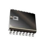
| 封装/外壳 | 16-TSSOP (0.173", 4.40mm 宽)裸焊盘 |
| 封装/箱体 | TSSOP-16 |
| 工作温度范围 | - 40 C to + 85 C |
| 工作电压 | 4.75 V to 5.5 V |
| 工作电流 | 135 mA |
| 工作电源电压 | 4.75 V to 5.5 V |
| 工厂包装数量 | 96 |
| 接口类型 | LO |
| 最大功率耗散 | 800 mW |
| 最大工作温度 | + 85 C |
| 最小工作温度 | - 40 C |
| 本底噪声 | -156dBm/Hz |
| 标准包装 | 96 |
| 测试频率 | 2.14GHz |
| 电压-电源 | 4.75 V ~ 5.5 V |
| 电流-电源 | 150mA |
| 电源电流 | 135 mA |
| 类型 | Modulator |
| 系列 | AD8349 |
| 视频文件 | http://www.digikey.cn/classic/video.aspx?PlayerID=1364138032001&width=640&height=505&videoID=2245193150001 |
| 调制类型 | Quadrature |
| 输出功率 | 5.1dBm |


- 商务部:美国ITC正式对集成电路等产品启动337调查
- 曝三星4nm工艺存在良率问题 高通将骁龙8 Gen1或转产台积电
- 太阳诱电将投资9.5亿元在常州建新厂生产MLCC 预计2023年完工
- 英特尔发布欧洲新工厂建设计划 深化IDM 2.0 战略
- 台积电先进制程称霸业界 有大客户加持明年业绩稳了
- 达到5530亿美元!SIA预计今年全球半导体销售额将创下新高
- 英特尔拟将自动驾驶子公司Mobileye上市 估值或超500亿美元
- 三星加码芯片和SET,合并消费电子和移动部门,撤换高东真等 CEO
- 三星电子宣布重大人事变动 还合并消费电子和移动部门
- 海关总署:前11个月进口集成电路产品价值2.52万亿元 增长14.8%


PDF Datasheet 数据手册内容提取
700 MHz to 2700 MHz Quadrature Modulator Data Sheet AD8349 FEATURES FUNCTIONAL BLOCK DIAGRAM Output frequency range: 700 MHz to 2700 MHz AD8349 Modulation bandwidth: dc to 160 MHz (large signal BW) IBBP 1 16 QBBP 1 dB output compression: 5.6 dBm @ 2140 MHz IBBN 2 15 QBBN Output disable function: output below –50 dBm in < 50 ns Noise floor: –156 dBm/Hz COM1 3 14 COM3 Phase quadrature error: 0.3 degrees @ 2140 MHz Σ Amplitude balance: 0.1 dB COM1 4 13 COM3 Single supply: 4.75 V to 5.5 V Pin compatible with AD8345/AD8346s LOIN 5 12 VPS2 16-lead, exposed-paddle TSSOP package PHASE LOIP 6 SPLITTER 11 VOUT APPLICATIONS VPS1 7 10 COM3 BIAS CeWlluClDarM/PAC/SC DcoMmAm20u0n0ic/aPtCioSn/G sSyMst/eEmDsG iEn frastructure ENOP 8 9 COM2 03570-0-001 Wireless LAN/wireless local loop Figure 1. LMDS/broadband wireless access systems PRODUCT DESCRIPTION The AD8349 is a silicon, monolithic, RF quadrature modulator The AD8349 can be used as a direct-to-RF modulator in digital that is designed for use from 700 MHz to 2700 MHz. Its communication systems such as GSM, CDMA, and WCDMA excellent phase accuracy and amplitude balance enable high base stations, and QPSK or QAM broadband wireless access performance direct RF modulation for communication systems. transmitters. Its high dynamic range and high modulation accuracy also make it a perfect IF modulator in local multipoint The differential LO input signal is buffered, and then split into distribution systems (LMDS) using complex modulation an in-phase (I) signal and a quadrature-phase (Q) signal using a formats. polyphase phase splitter. These two LO signals are further buffered and then mixed with the corresponding I channel and The AD8349 is fabricated using Analog Devices’ advanced Q channel baseband signals in two Gilbert cell mixers. The complementary silicon bipolar process, and is available in a 16- mixers’ outputs are then summed together in the output lead, exposed-paddle TSSOP package. Its performance is amplifier. The output amplifier is designed to drive 50 Ω loads. specified over a –40°C to +85°C temperature range. The RF output can be switched on and off within 50 ns by applying a control pulse to the ENOP pin. Rev. B Information furnished by Analog Devices is believed to be accurate and reliable. However, no responsibility is assumed by Analog Devices for its use, nor for any infringements of patents or other One Technology Way, P.O. Box 9106, Norwood, MA 02062-9106, U.S.A. rights of third parties that may result from its use. Specifications subject to change without notice. No license is granted by implication or otherwise under any patent or patent rights of Analog Devices. Tel: 781.329.4700 www.analog.com Trademarks and registered trademarks are the property of their respective owners. Fax: 781.461.3113 ©2003–2012 Analog Devices, Inc. All rights reserved.
AD8349 Data Sheet TABLE OF CONTENTS Features .............................................................................................. 1 Single-Ended LO Drive ............................................................. 17 Applications ....................................................................................... 1 RF Output .................................................................................... 17 Functional Block Diagram .............................................................. 1 Output Enable ............................................................................. 17 Product Description ......................................................................... 1 Baseband DAC Interface ........................................................... 18 Revision History ............................................................................... 2 AD9777 Interface ....................................................................... 18 Specifications ..................................................................................... 3 Biasing and Filtering .................................................................. 18 Absolute Maximum Ratings ............................................................ 5 Reducing Undesired Sideband Leakage .................................. 19 ESD Caution .................................................................................. 5 Reduction of LO Feedthrough .................................................. 19 Pin Configuration and Function Descriptions ............................. 6 Sideband Suppression and LO Feedthrough vs. Equivalent Circuits ........................................................................... 7 Temperature ................................................................................ 20 Typical Performance Characteristics ............................................. 8 Single Sideband Performance vs. Baseband Drive Level ...... 20 Circuit Description ......................................................................... 14 Improving Third Harmonic Distortion .................................. 20 Overview ...................................................................................... 14 Applications ..................................................................................... 21 LO Interface................................................................................. 14 3GPP WCDMA Single-Carrier Application ........................... 21 V-to-I Converter ......................................................................... 14 WCDMA MultiCarrier Application ........................................ 21 Mixers .......................................................................................... 14 GSM/EDGE Application ........................................................... 22 D-to-S Amplifier ......................................................................... 14 Soldering Information ............................................................... 23 Bias Circuit .................................................................................. 14 LO Generation Using PLLs ....................................................... 23 Output Enable ............................................................................. 14 Transmit DAC Options ............................................................. 23 Basic Connections .......................................................................... 15 Evaluation Board ............................................................................ 24 Baseband I and Q Inputs ........................................................... 15 Characterization Setups ................................................................. 26 Single-Ended Baseband Drive .................................................. 15 SSB Setup ..................................................................................... 26 LO Input Drive Level ................................................................. 16 Outline Dimensions ....................................................................... 27 Frequency Range ........................................................................ 16 Ordering Guide .......................................................................... 27 LO Input Impedance Matching ................................................ 16 REVISION HISTORY 2/12—Rev. A to Rev. B Added EPAD Note ............................................................................ 6 Changes to Ordering Guide .......................................................... 27 11/04—Data Sheet Changed from Rev. 0 to Rev. A Changes to Figure 25 through Figure 30 ..................................... 11 Changes to Figure 37 through Figure 39 ..................................... 13 Change to WCDMA MultiCarrier Application section ............ 21 Change to Figure 60 and Figure 61 .............................................. 21 11/03—Revision 0: Initial Version Rev. B | Page 2 of 28
Data Sheet AD8349 SPECIFICATIONS V = 5 V; ambient temperature (T ) = 25°C; LO = –6 dBm; I/Q inputs = 1.2 V p-p differential sine waves in quadrature on a 400 mV dc S A bias; baseband frequency = 1 MHz; LO source and RF output load impedances are 50 Ω, unless otherwise noted. Table 1. Parameter Conditions Min Typ Max Unit Operating Frequency 700 2700 MHz LO = 900 MHz Output Power 1.5 4 6 dBm Output P1 dB 7.6 dBm Carrier Feedthrough –45 –30 dBm Sideband Suppression –35 –31 dBc Third Harmonic1 P – (F + (3 × F )), P = 4 dBm –39 –36 dBc OUT LO BB OUT Output IP3 F1 = 3 MHz, F2 = 4 MHz, P = -4.2 dBm 21 dBm BB BB OUT Quadrature Error 1.9 degree I/Q Amplitude Balance 0.1 dB Noise Floor 20 MHz offset from LO, all BB inputs 400 mV dc bias only –155 dBm/Hz 20 MHz offset from LO, BB inputs = 1.2 V p-p differential on 400 mV dc –150 dBm/Hz GSM Sideband Noise LO = 884.8 MHz, 6 MHz offset from LO, P = 2 dBm –152 dBc/Hz OUT LO = 1900 MHz Output Power 0 3.8 6 dBm Output P1dB 6.8 dBm Carrier Feedthrough –38 dBm Sideband Suppression –40 –36 dBc Third Harmonic 1 P – (F + (3 × F )), P = 3.8 dBm –37 –36 dBc OUT LO BB OUT Output IP3 F1 = 3 MHz, F2 = 4 MHz, P = –4.5 dBm 22 dBm BB BB OUT Quadrature Error 0.7 degree I/Q Amplitude Balance 0.1 dB Noise Floor 20 MHz offset from LO, all BB inputs 400 mV dc bias only –156 dBm/Hz 20 MHz offset from LO, BB inputs = 1.2 V p-p differential on 400 mV dc –150 dBm/Hz GSM Sideband Noise LO = 1960 MHz, 6 MHz offset from LO, P = 2 dBm –151 dBc/Hz OUT LO = 2140 MHz Output Power –2 2.4 5.1 dBm Output P1dB 5.6 dBm Carrier Feedthrough –42 –30 dBm Sideband Suppression –43 –36 dBc Third Harmonic 1 P – (F + (3 × F )), P = 2.4 dBm –37 –36 dBc OUT LO BB OUT Output IP3 F1 = 3 MHz, F2 = 4 MHz, P = –6.5 dBm 19 dBm BB BB OUT Quadrature Error 0.3 degree I/Q Amplitude Balance 0.1 dB Noise Floor 20 MHz offset from LO, all BB inputs 400 mV dc bias only –156 dBm/Hz 20 MHz offset from LO, BB inputs = 1.2 V p-p differential on 400 mV dc –151 dBm/Hz WCDMA Noise Floor LO = 2140 MHz. 30 MHz offset from LO, P = –17.3 dBm –156 dBm/Hz CHAN LO INPUTS Pins LOIP and LOIN LO Drive Level Characterization performed at typical level –10 –6 0 dBm Nominal Impedance 50 Ω Input Return Loss Drive via 1:1 balun, LO = 2140 MHz –8.6 dB BASEBAND INPUTS Pins IBBP, IBBN, QBBP, QBBN I and Q Input Bias Level 400 mV Input Bias Current 11 µA Input Offset Current 1.8 µA Bandwidth (0.1 dB) LO = 1500 MHz, baseband input = 600 mV p-p sine wave on 400 mV dc 10 MHz LO = 1500 MHz, baseband input = 60 mV p-p sine wave on 400 mV dc 24 MHz Rev. B | Page 3 of 28
AD8349 Data Sheet Parameter Conditions Min Typ Max Unit Bandwidth (3 dB) LO = 1500 MHz, baseband input = 600 mV p-p sine wave on 400 mV dc 160 MHz LO = 1500 MHz, baseband input = 60 mV p-p sine wave on 400 mV dc 340 MHz OUTPUT ENABLE Pin ENOP Off Isolation ENOP Low –78 –50 dBm Turn-On Settling Time ENOP Low to High (90% of envelope) 20 ns Turn-Off Settling Time ENOP High to Low (10% of envelope) 50 ns ENOP High Level (Logic 1) 2.0 V ENOP Low Level (Logic 0) 0.8 V POWER SUPPLIES Pins VPS1 and VPS2 Voltage 4.75 5.5 V Supply Current ENOP = High 135 150 mA ENOP = Low 130 145 mA 1 The amplitude of the third harmonic relative to the single sideband power decreases with decreasing baseband drive level (see Figure 19, Figure 20, and Figure 21). Rev. B | Page 4 of 28
Data Sheet AD8349 ABSOLUTE MAXIMUM RATINGS tresses above those listed under Absolute Maximum Ratings Table 2. may cause permanent damage to the device. This is a stress Parameter Rating rating only; functional operation of the device at these or any Supply Voltage VPOS 5.5 V other conditions above those indicated in the operational IBBP, IBBN, QBBP, QBBN 0 V, 2.5 V section of this specification is not implied. Exposure to absolute LOIP and LOIN 10 dBm maximum rating conditions for extended periods may affect Internal Power Dissipation 800 mW device reliability. θ (Exposed Paddle Soldered Down) 30°C/W JA Maximum Junction Temperature 125°C ESD CAUTION Operating Temperature Range −40°C to +85°C Storage Temperature Range −65°C to +150°C Rev. B | Page 5 of 28
AD8349 Data Sheet PIN CONFIGURATION AND FUNCTION DESCRIPTIONS IBBP 1 16 QBBP IBBN 2 15 QBBN COM1 3 14 COM3 AD8349 COM1 4 13 COM3 TOP VIEW LOIN 5 (Not to Scale) 12 VPS2 LOIP 6 11 VOUT EVNPOSP1 78 190 CCOOMM32 03570-0-002 NOTES 1.CONNECT EXPOSED PAD TO THE GROUND LANE VIA A LOW IMPEDANCE PATH. Figure 2. Table 3. Pin Function Descriptions Equivalent Pin No. Mnemonic Description Circuit 1, 2, IBBP, IBBN, Differential In-Phase and Quadrature Baseband Inputs. These high impedance inputs must be Circuit A 15, 16 QBBN, QBBP dc-biased to approximately 400 mV dc, and must be driven from a low impedance source. Nominal characterized ac signal swing is 600 mV p-p on each pin (100 mV to 700 mV). This results in a differential drive of 1.2 V p-p with a 400 mV dc bias. These inputs are not self-biased and must be externally biased. 3, 4 COM1 Common Pin for LO Phase Splitter and LO Buffers. COM1, COM2, and COM3 should all be connected to a ground plane via a low impedance path. 5, 6 LOIN, LOIP Differential Local Oscillator Inputs. Internally dc-biased to approximately 1.8 V when V = 5.0 V. Circuit B S Pins must be ac-coupled. Single-ended drive is possible with degradation in performance. 7 VPS1 Positive Supply Voltage (4.75 V to 5.5 V) for the LO Bias-Cell and Buffer. VPS1 and VPS2 should be connected to the same supply. To ensure adequate external bypassing, connect 0.1 μF and 100 pF capacitors between VPS1 and ground. 8 ENOP Output Enable. This pin can be used to enable or disable the RF output. Connect to high logic Circuit C level for normal operation. Connect to low logic level to disable output. 9 COM2 Common Pin for the Output Amplifier. COM1, COM2, and COM3 should all be connected to a ground plane via a low impedance path. 10, 13, COM3 Common Pin for Input V-to-I Converters and Mixer Cores. COM1, COM2, and COM3 should all be 14 connected to a ground plane via a low impedance path. 11 VOUT Device Output. Single-ended, 50 Ω internally biased RF output. Pin must be ac-coupled to the Circuit D load. 12 VPS2 Positive Supply Voltage (4.75 V to 5.5 V) for the Baseband Input V-to-I Converters, Mixer Core, Band Gap Reference, and Output Amplifer. VPS1 and VPS2 should be connected to the same supply. To ensure adequate external bypassing, connect 0.1 μF and 100 pF capacitors between VPS2 and ground. EP Exposed Paddle. Connect to the ground plane via a low impedance path. Rev. B | Page 6 of 28
Data Sheet AD8349 EQUIVALENT CIRCUITS VPS2 VPS2 ENOP IBBP COM3 03570-0-003 COM3 04500-0-005 Figure 3. Circuit A Figure 5. Circuit C VPS1 VPS2 LOIN 40Ω VOUT LOIP 40Ω 03570-0-006 COM2 COM1 03570-0-004 Figure 4. Circuit B Figure 6. Circuit D Rev. B | Page 7 of 28
AD8349 Data Sheet TYPICAL PERFORMANCE CHARACTERISTICS 8 10 7 VS = 5.25V 9 6 VS = 5V m) 8 ER (dBm) 45 SSION (dB 576 TT == ++8255CC TPUT POW 321 VS = 4.75V T COMPRE 324 T =–40C U U 1 O 0 P SSB –1 B OUT –10 –2 1d –2 –3 –3 –4700 900 1100 130L0O1 F5R0E0Q1U7E0N0CY19 (0M0Hz2)100 2300 2500 2700 03570-0-007 –4700 900 1100 130L0O1 F5R0E0Q1U7E0N0CY19 (0M0Hz2)100 2300 2500 2700 03570-0-010 Figure 7. Single Sideband (SSB) Output Power (POUT) vs. LO Frequency (FLO) Figure 10. SSB Output 1 dB Compression Point (OP1dB) vs. FLO (FBB = 1 MHz, (I and Q Inputs Driven in Quadrature at Baseband Frequency (FBB) = 1 MHz, I and Q Inputs Driven in Quadrature , TA = 25°C) I and Q Inputs at 1.2 V p-p Differential, TA = 25°C) 1 –10 0 –15 60mV p-p B) –1 m) –20 RIATION (d ––32 OUGH (dB ––3205 OWER VA ––54 600mV p-p FEEDTHR ––4305 VS = 5V VS = 5.25V OUTPUT P –––786 CARRIER ––5405 VS = 4.75V –9 –55 –101 BAS1E0BAND FREQUENCY1 0(M0Hz) 1000 03570-0-008 –60700 900 1100 130L0O1 F5R0E0Q1U7E0N0CY19 (0M0Hz2)100 2300 2500 2700 03570-0-011 Figure 8. I and Q Input Bandwidth Normalized to Gain @ 1 MHz Figure 11. Carrier Feedthrough vs. FLO (FBB = 1 MHz, I and Q Inputs Driven in (FLO = 1500 MHz, TA = 25°C) Quadrature at 1.2 V p-p Differential, TA = 25°C) –20 4.0 –22 –24 3.5 m) –26 ER (dBm) 23..50 VS = 5.25VVS = 5V OUGH (dB –––332208 W R PUT PO 2.0 VS = 4.75V FEEDTH –––333864 VS = 5.25V VS = 5V SSB OUT 11..05 CARRIER –––444420 VS = 4.75V –46 0.5 –48 0–40 –30 –20 –10 0TE1M0PER2A0TU3R0E (4C0) 50 60 70 80 03570-0-009 –50–40 –30 –20 –10 0TE1M0PER2A0TU3R0E (4C0) 50 60 70 80 03570-0-012 Figure 9. SSB POUT vs. Temperature (FLO = 2140 MHz, FBB = 1 MHz, I and Q Figure 12. Carrier Feedthrough vs. Temperature (FLO = 2140 MHz, FBB = 1 MHz, Inputs Driven in Quadrature at 1.2 V p-p Differential) I and Q Inputs Driven in Quadrature at 1.2 V p-p Differential, TA = 25°C) Rev. B | Page 8 of 28
Data Sheet AD8349 –10 –10 –15 –15 Bc) –20 Bc) –20 N (d –25 N (d –25 O O ESSI –30 VS = 5.25V ORTI –30 VS = 5V VS = 4.75V R T PP –35 VS = 4.75V DIS –35 DEBAND SU ––4450 VS = 5V RD ORDER ––4450 VS = 5.25V SI –50 HI –50 T –55 –55 –60700 900 1100 130L0O1 F5R0E0Q1U7E0N0CY19 (0M0Hz2)100 2300 2500 2700 03570-0013 –60700 900 1100 130L0O1 F5R0E0Q1U7E0N0CY19 (0M0Hz2)100 2300 2500 2700 03570-0016 Figure 13. Sideband Suppression vs. FLO (FBB = 1 MHz, I and Q Inputs Figure 16. Third Order Distortion vs. FLO (FBB = 1 MHz, I and Q Inputs Driven in Quadrature at 1.2 V p-p Differential, TA = 25°C) Driven in Quadrature at 1.2 V p-p Differential, TA = 25°C) –10 –10 –15 VS = 4.75V –15 PPRESSION (dBc) ––––33225050 VS = 5.25V DISTORTION (dBc) ––––33225050 VS = 5V D SU –40 DER –40 SIDEBAN ––5405 VS = 5V THIRD OR ––5405 VS = 5.25V VS = 4.75V –55 –55 –601 BASEBAND FR1E0QUENCY (MHz) 100 03570-0-014 –601 BASEBAND FR1E0QUENCY (MHz) 100 03570-0-017 Figure 14. Sideband Suppression vs. FBB (FLO = 2140 MHz, I and Q Inputs Figure 17. Third Order Distortion vs. FBB (FLO = 2140 MHz, I and Q Inputs Driven in Quadrature at 1.2 V p-p Differential, TA = 25°C) Driven in Quadrature at 1.2 V p-p Differential, TA = 25°C) –30 –30 VS = 4.75V VS = 5V PPRESSION (dBc) –––443505 VS = 5V VS = 4.75V DISTORTION (dBc) –––443505 VS = 5.25V D SU VS = 5.25V DER AN –50 OR –50 SIDEB –55 THIRD –55 –60–40 –30 –20 –10 0TE1M0PER2A0TU3R0E (°4C0) 50 60 70 80 03570-0-015 –60–40 –30 –20 –10 0TE1M0PER2A0TU3R0E (°4C0) 50 60 70 80 03570-0-018 Figure 15. Sideband Suppression vs. Temperature (FLO = 2140 MHz, Figure 18. Third Order Distortion vs. Temperature (FLO = 2140 MHz, FBB = 1 MHz, I and Q Inputs Driven in Quadrature at 1.2 V p-p Differential) FBB = 1 MHz, I and Q Inputs Driven in Quadrature at 1.2 V p-p Differential) Rev. B | Page 9 of 28
AD8349 Data Sheet –10 10 160 3USB, dBc –15 SSB, dBm 8 155 –20 6 150 ––3205 24 T (mA) 145 VS = 5V –35 0 EN 140 –40 USB, dBC –2 URR 135 VS = 5.25V C –45 –4 LY 130 –50 –6 PP VS = 4.75V LO, dBm U 125 –55 –8 S 120 –60 –10 –65 –12 115 –700.2 0.4BA0S.6EB0A.8ND1 D.0IF1F.E2RE1N.4TI1A.L6 IN1P.8UT2 .V0OL2T.2AG2E.4 (V2 .p6-p)2.8 3.0–14 03570-0-019 110–40 –30 –20 –10 0TE1M0PER2A0TU3R0E (°4C0) 50 60 70 80 03570-0-022 Figure 19. Third Order Distortion (3USB), Carrier Feedthrough, Sideband Figure 22. Power Supply Current vs. Temperature Suppression, and SSB POUT vs. Baseband Differential Input Level (FLO = 900 MHz, FBB = 1 MHz, I and Q Inputs Driven in Quadrature, TA = 25°C) –10 10 –15 8 SSB, dBm –20 6 –25 4 –30 2 500Ω –35 LO, dBm 0 200Ω –40 –2 –45 –4 –50 USB, dBc –6 3USB, dBc –55 –8 –60 –10 NO TERMINATION –65 –12 –700.2 0.4BA0S.6EB0A.8ND1 D.0IF1F.E2RE1N.4TI1A.L6 IN1P.8UT2 .V0OL2T.2AG2E.4 (V2 .p6-p)2.8 3.0–14 03570-0-020 03570-0023 Figure 20. Third Order Distortion (3USB), Carrier Feedthrough, Sideband Figure 23. Smith Chart of LOIP Port S11 (LOIN Pin AC-Coupled Suppression, and SSB POUT vs. Baseband Differential Input Level to Ground). Curves with Balun and External Termination (FLO = 1900 MHz, FBB = 1 MHz, I and Q Inputs Driven in Quadrature, TA = 25°C) Resistors Also Shown (TA = 25°C) –10 10 0 3USB, dBc –15 8 SSB, dBm –5 –20 6 –25 4 –10 –30 2 –15 VS = 5V –35 0 B) –40 LO, dBm –2 S (d –20 S O –45 –4 L N –25 –50 –6 UR –55 USB, dBc –8 RET –30 –60 –10 –35 –65 –12 –700.2 0.4BA0S.6EB0A.8ND1 D.0IF1F.E2RE1N.4TI1A.L6 IN1P.8UT2 .V0OL2T.2AG2E.4 (V2 .p6-p)2.8 3.0–14 03570-0-021 –40700 900 1100 1300F1R5E0Q0UE17N0C0Y 1(M90H0z)2100 2300 2500 2700 03570-0-024 Figure 21. Third Order Distortion (3USB), Carrier Feedthrough, Sideband Figure 24. Return Loss S22of VOUT Output (TA = 25°C) Suppression, and SSB POUT vs. Baseband Differential Input Level (FLO = 2140 MHz, FBB = 1 MHz, I and Q Inputs Driven in Quadrature, TA = 25°C) Rev. B | Page 10 of 28
Data Sheet AD8349 30 20 28 18 26 24 16 22 14 20 E E G 18 G 12 A A CENT 1146 CENT 10 R R E 12 E 8 P P 10 6 8 6 4 4 2 2 0–157.0 –156.5 –156.0 NO–155.5ISE FLO–155.0OR (dBm–154.5/Hz) –154.0 –153.5 –153.0 03570-0-025 0–152.0 –151.5 –151.0 –150.5NOIS–150.0E FLO–149.5OR (d–149.0Bm/Hz–148.5) –148.0 –147.5 –147.0 03570-0-028 Figure 25. 20 MHz Offset Noise Floor Distribution at FLO = 900 MHz Figure 28. 20 MHz Offset Noise Floor Distribution at FLO = 940 MHz (BB Inputs at a Bias of 400 mV with no AC signal, TA = 25°C) (FBB = 1 MHz, I and Q Inputs Driven in Quadrature at 1.2 V p-p, TA = 25°C) 30 28 28 26 26 24 24 22 22 20 20 E E 18 G 18 G A A 16 CENT 1146 CENT 14 R R 12 E 12 E P P 10 10 8 8 6 6 4 4 2 2 0–158.0 –157.5 –157.0 NO–156.5ISE FLO–156.0OR (dBm–155.5/Hz) –155.0 –154.5 –154.0 03570-0-026 0–152.5 –152.0 –151.5 N–151.0OISE F–150.5LOOR–150.0 (dBm/H–149.5z) –149.0 –148.5 –148.0 03570-0-029 Figure 26. 20 MHz Offset Noise Floor Distribution at FLO = 1900 MHz Figure 29. 20 MHz Offset Noise Floor Distribution at FLO = 1960 MHz (BB Inputs at a Bias of 400 mV with no AC signal, TA = 25°C) (FBB = 1 MHz, I and Q Inputs Driven in Quadrature at 1.2 V p-p, TA = 25°C) 30 30 28 28 26 26 24 24 22 22 20 20 E E G 18 G 18 A A NT 16 NT 16 CE 14 CE 14 R R E 12 E 12 P P 10 10 8 8 6 6 4 4 2 2 0–159.0 –158.5 –158.0 NO–157.5ISE FLO–157.0OR (dBm–156.5/Hz) –156.0 –155.5 –155.0 03570-0-027 0–153.0 –152.5 –152.0 NO–151.5ISE FLO–151.0OR (dBm–150.5/Hz) –150.0 –149.5 –149.0 03570-0-030 Figure 27. 20 MHz Offset Noise Floor Distribution at FLO = 2140 MHz Figure 30. 20 MHz Offset Noise Floor Distribution at FLO = 2140 MHz (BB Inputs at a Bias of 400 mV with no AC signal, TA = 25°C) (FBB = 1 MHz, I and Q Inputs Driven in Quadrature at 1.2 V p-p, TA = 25°C) Rev. B | Page 11 of 28
AD8349 Data Sheet –140 35 –142 30 –144 Hz)–146 25 m/ SE FLOOR (dB–––111545082 WITH AC INPUT PERCENTAGE 1250 NOI–154 WITHOUT AC INPUT 10 –156 5 –158 –160–10 –8 –6 LO INP–U4T (dBm)–2 0 2 03570-0-031 –00.200 –0.175 –0.1M50AG–N0I.T1U25DE– I0M.1B0A0LA–0N.C07E5 (d–B0).050 –0.025 0 03570-0-034 Figure 31. 20 MHz Offset Noise Floor vs. LO Input Power Figure 34. I and Q Inputs Quadrature Phase Imbalance Distribution (FLO = 2140 MHz, TA = 25°C) (FLO = 2140 MHz, FBB = 1 MHz, I and Q Inputs Driven in Quadrature at 1.2 V p-p Differential, TA = 25°C) –10 35 –15 30 m) –20 B d H ( –25 25 G U E O –30 G THR –35 FLO = 1900MHz NTA 20 D E FEE –40 ERC 15 R P RIE –45 10 R FLO = 2140MHz CA –50 –55 FLO = 900MHz 5 –60–10 –8 –6 LO INP–U4T (dBm)–2 0 2 03570-0032 00 0.25 PHAS0E.5 (0I-Q) IMB0A.7L5ANCE (1D.0e0grees)1.25 1.50 03570-0-035 Figure 32. Carrier Feedthrough vs. LO Input Power (FBB = 1 MHz, I and Q Figure 35. I and Q Inputs Amplitude Imbalance Distribution Inputs Driven in Quadrature at 1.2 V p-p Differential, TA = 25°C) (FLO = 2140 MHz, FBB = 1 MHz, I and Q Inputs Driven in Quadrature at 1.2 V p-p Differential, TA = 25°C) –10 35 –15 30 Bc) –20 FLO = 900MHz d N ( –25 25 O ESSI –30 FLO = 1900MHz AGE 20 R T P –35 N P E U C ND S –40 PER 15 A B –45 10 DE FLO = 2140MHz SI –50 5 –55 –60–10 –8 –6 LO INP–U4T (dBm)–2 0 2 03570-0033 04.5 5.0 OP1d5B.5 (dBm) 6.0 6.5 03570-0-036 Figure 33. Sideband Suppression vs. LO Input Power (FBB = 1 MHz, I and Q Figure 36. OP1dB Distribution. (FLO = 2140 MHz, FBB = 1 MHz, I and Q Inputs Inputs Driven in Quadrature at 1.2 V p-p Differential, TA = 25°C) Driven in Quadrature, TA = 25°C) Rev. B | Page 12 of 28
Data Sheet AD8349 20 35 18 T = +85°C 30 T =–40°C 16 14 25 E E G 12 G A A 20 T T EN 10 EN C C R R 15 E 8 E P P 6 10 4 5 2 0–80 –70CARRIER–6 F0EEDTHRO–U5G0H (dBm)–40 –30 03570-0-039 0–70 –A6F5TCEARR NRUIELLR–I6 NF0GEE TDOT H<R–6O–5U5dG5BHm ( AdBT m+2)5–°5C0 –45 03570-0-037 Figure 37. Carrier Feedthrough Distribution at FLO = 900 MHZ (FBB = 1 MHz, Figure 40. Carrier Feedthrough Distribution at Temperature Extremes, After I and Q Inputs Driven in Quadrature at 1.2 V p-p, TA = 25°C) Carrier Feedthrough Nulled to < - 65 dBm at TA = 25°C. (FLO = 2140 MHz, I and Q Inputs at a bias of 400 mV) 40 30 28 T = +85°C 35 26 T =–40°C 24 30 22 20 E 25 E G G 18 A A CENT 20 CENT 1164 R R PE 15 PE 12 10 10 8 6 5 4 2 0–60 –55 C–A5R0RIER –F4E5EDTHR–O40UGH (d–B35m) –30 –25 03570-0-040 0–75 –70 AF–T6SE5IRD ENBUA–L6NL0IDN GSU T–PO5P 5<RE–S50S–dI5OB0Nc A(dTB –+c42)55°C –40 –35 03570-0-038 Figure 38. Carrier Feedthrough Distribution at FLO = 1900 MHz (FBB = 1 MHz, Figure 41. Sideband Suppression Distribution at Temperature Extremes, After I and Q Inputs Driven in Quadrature at 1.2 Vp-p, TA = 25°C) Sideband Suppression Nulled to < -50 dBc at TA = 25°C. (FLO = 2140 MHz, FBB = 1 MHz, I and Q Inputs biased at 0.4 V) 24 22 20 18 16 E G A 14 T N E 12 C ER 10 P 8 6 4 2 –070 –65 –C60ARRI–E5R5 FEED–T50HROU–G4H5 (dBm–4)0 –35 –30 03570-0-041 Figure 39. Carrier Feedthrough Distribution at FLO = 2140 MHz (FBB = 1 MHz, I and Q Inputs Driven in Quadrature at 1.2 V p-p, TA = 25°C) Rev. B | Page 13 of 28
AD8349 Data Sheet CIRCUIT DESCRIPTION OVERVIEW V-TO-I CONVERTER The AD8349 can be divided into five sections: the local oscil- The differential baseband input voltages that are applied to the lator (LO) interface, the baseband voltage-to-current (V-to-I) baseband input pins are fed to two op amps that perform a converter, the mixers, the differential-to-single-ended (D-to-S) differential voltage-to-current conversion. The differential amplifier, and the bias circuit. A detailed block diagram of the output currents of these op amps then feed each of their device is shown in Figure 42. respective mixers. MIXERS LOIP PHASE The AD8349 has two double-balanced mixers, one for the in- LOIN SPLITTER phase channel (I channel) and one for the quadrature channel (Q channel). Both mixers are based on the Gilbert cell design of IBBP four cross-connected transistors. The output currents from the IBBN two mixers sum together in a pair of resistor-inductor (R-L) Σ OUT loads. The signals developed across the R-L loads are sent to the QQBBBBNP 03570-0-043 DD--tToO-S- aSm ApMlifiPerL. IFIER Figure 42. Block Diagram The output D-to-S amplifier consists of two emitter followers The LO interface generates two LO signals at 90 degrees of driving a totem pole output stage. Output impedance is estab- phase difference to drive two mixers in quadrature. Baseband lished by the emitter resistors in the output transistors. The signals are converted into currents by the V-to-I converters, output of this stage connects to the output (VOUT) pin. which feed into the two mixers. The outputs of the mixers combine to feed the differential-to-single-ended amplifier, BIAS CIRCUIT which provides a 50 Ω output interface. Reference currents to A band gap reference circuit generates the proportional-to- each section are generated by the bias circuit. Additionally, the absolute-temperature (PTAT) reference currents used by RF output is controlled by an output enable pin (ENOP), which different sections. The band gap reference circuit also generates is capable of switching the output on and off within 50 ns. A a temperature stable current in the V-to-I converters to produce detailed description of each section follows. a temperature independent slew rate. LO INTERFACE OUTPUT ENABLE The LO interface consists of interleaved stages of buffer During normal operation (ENOP = high), the output current amplifiers and polyphase phase splitters. An input buffer from the V-to-I converters feeds into the mixers, where they provides a 50 Ω termination to the LO signal source driving mix with the two phases of LO signals. When ENOP is pulled LOIP and LOIN. The buffer also increases the LO signal low, the V-to-I output currents are steered away from the amplitude to drive the phase splitter. The phase splitter is mixers, thus turning off the RF output. Power to the final stage formed by an R-C polyphase network that splits the buffered of LO drivers is also removed to minimize LO feedthrough. LO signal into two parts in precise quadrature phase relation Even when the output is disabled, the differential-to-single- with each other. Each LO signal then passes through a buffer ended stage is still powered up to maintain constant output amplifier to compensate for the signal loss through the phase impedance. splitter. The two signals pass through another polyphase network to enhance the quadrature accuracy over the full operating frequency range. The outputs of the second phase splitter are fed into the driver amplifiers for the mixers’ LO inputs. Rev. B | Page 14 of 28
Data Sheet AD8349 BASIC CONNECTIONS The basic connections for operating the AD8349 are shown in power of the output signal is at least a crest factor below the Figure 43. A single power supply of between 4.75 V and 5.5 V is AD8349’s output compression point. Refer to the Applications applied to pins VPS1 and VPS2. A pair of ESD protection section for drive-level considerations in WCDMA and diodes connect internally between VPS1 and VPS2, so these GSM/EDGE systems. must be tied to the same potential. Both pins should be Reducing the baseband drive level also has the benefit of individually decoupled using 100 pF and 0.1 μF capacitors to increasing the bandwidth of the baseband input. This would ground. These capacitors should be located as close as possible allow the AD8349 to be used in applications requiring a high to the device. For normal operation, the output enable pin, modulation bandwidth, e.g., as the IF modulator in high data- ENOP, must be pulled high. The turn-on threshold for ENOP is rate microwave radios. 2 V. Pins COM1, COM2, and COM3 should all be tied to the SINGLE-ENDED BASEBAND DRIVE same ground plane through low impedance paths. BASEBAND I AND Q INPUTS Where only single-ended I and Q signals are available, a differential amplifier, such as the AD8132 or AD8138, can be The I and Q inputs should be driven differentially. The typical used to generate the required differential drive signal for the differential drive level (as used for characterization measure- AD8349. ments) for the I and Q baseband signals is 1.2 V p-p, which is Figure 44 shows an example of a circuit that converts a ground- equivalent to 600 mV p-p on each baseband input. The base- referenced, single-ended signal to a differential signal, and adds band inputs have to be externally biased to a level between the required 400 mV bias voltage. 400 mV and 500 mV. The optimum level for the best perfor- mance is 400 mV. The recommended drive level of 1.2 V p-p The baseband inputs can also be driven with a single-ended does not indicate a maximum drive level. If operation closer to signal biased to 400 mV, with the unused inputs biased to compression is desired, the 1.2 V p-p differential limit can be 400 mV dc. This mode of operation is not recommended, exceeded. however, because any dc level difference between the bias level of the drive signal and the dc level on the unused input For baseband signals with a high peak-to-average ratio (e.g., (including the effect of temperature drift), can result in CDDA or WCDMA), the peak signal level will have to be below increased LO feedthrough. Additionally, the maximum low the AD8349’s compression level in order to prevent clipping of distortion output power will be reduced by 6 dB. the signal peaks. Clipping of signal peaks increases distortion. In the case of CDMA and WCDMA inputs, clipping results in an increase of signal leakage into adjacent channels. In general, the baseband drive should be at a level where the peak signal IP 1 IBBP QBBP 16 QP 2 IBBN QBBN 15 IN QN 3 COM1 COM3 14 200Ω 4 COM1 COM3 13 5 1 AD8349 +VS T1 100pF 5 LOIN VPS2 12 100pF 0.1µF ETC1-1-13 2 100pF 6 LOIP VOUT 11 VOUT LO 4 3 100pF 7 VPS1 COM3 10 200Ω +VS 8 ENOP COM2 9 03570-0-044 0.1µF 100pF Figure 43. Basic Connections Rev. B | Page 15 of 28
AD8349 Data Sheet +5V 10kΩ + 866Ω 0.1µF 10µF 0.1µF 100pF 100pF 0.1µF 499Ω IIN 499Ω 8 3 5 49.9Ω 2 AD8132 0.1µF 499Ω 4 VPS1 VPS2 1 6 IBBP 24.8Ω + 0.1µF 10µF IBBN Σ VOUT 499Ω –5V LOIP PHASE +5V QBBP SPLITTER LOIN QBBN + 0.1µF 10µF AD8349 499Ω COM1 COM2 COM3 QIN 499Ω 8 3 5 49.9Ω 2 AD8132 0.1µF 499Ω 4 1 6 24.9Ω + 499Ω 0.1µF 10µF 03570-0-045 –5V Figure 44. Single-Ended IQ Drive Circuit LO INPUT DRIVE LEVEL LO INPUT IMPEDANCE MATCHING The local oscillator inputs are designed to be driven differen- Single-ended LO sources are transformed into a differential tially. The device is specified with an LO drive level of –6 dBm. signal via a 1:1 balun (ETC1-1-13). A 200 Ω shunt resistor to This level was chosen to provide the best noise performance. GND on each LO input on the device side of the balun reduces Increasing the LO drive level degrades sideband suppression the return loss for the LO input port. Because the LO input pins and increases carrier feedthrough, while improving noise are internally dc-biased, ac coupling capacitors must be used on performance. Reducing the LO drive level creates the opposite each LO input pin. effect: improved sideband suppression and reduced carrier feedthrough. FREQUENCY RANGE The LO frequency range is from 700 MHz to 2700 MHz. These limits are defined by the nature of the LO phase splitter circuitry. The phase splitter generates LO drive signals for the internal mixers, which are 90 degrees out of phase from each other. Outside of the specified frequency range (700 MHz to 2700 MHz), this quadrature accuracy degrades, resulting in poor sideband rejection performance. Figure 45 and Figure 46 show the sideband suppression of a typical device operating outside the specified LO frequency range. The level of sideband suppression and degradation is also influenced by manufac- turing process variations. Rev. B | Page 16 of 28
Data Sheet AD8349 4.0 0 –10 –15 3.5 –10 c) m) –20 m) dB dB WER (dB 3.0 SSB –20 ESSION ( ROUGH ( ––3205 SINGLE-ENDED LO DRIVE O R H TPUT P 2.5 –30 D SUPP FEEDT ––4305 SSB OU 12..50 USB ––5400 SIDEBAN CARRIER ––5405 DIFFERENTIAL LO DRIVE 1.0300 350 400 LO4 5F0REQU5E00NCY (5M5H0z) 600 650 700–60 03570-0-046 ––6505700 900 1100 130L0O1 F5R0E0Q1U7E0N0CY19 (0M0Hz2)100 2300 2500 2700 03570-0-049 Figure 45. Sideband Suppression below 700 MHz Figure 48. LO Feedthrough vs. Frequency, Single-Ended vs. Differential LO 0 –40 Drive (Single-Sideband Modulation) –1 –41 RF OUTPUT m) –2 USB –42 dBc) The RF output is designed to drive a 50 Ω load, but should be dB N ( ac-coupled, as shown in Figure 43, because of internal dc WER ( –3 –43 ESSIO biasing. The RF output impedance is close to 50 Ω and provides UTPUT PO ––54 SSB ––4445 ND SUPPR frcaairinrcgluyei tg(rosyeo eids F rrieegqtuuurrienr e2 ld4o )si.fs Atohsve ea ro rutehtspeu ulsttp, iensc odi fraieidvddi niotgpio eanr 5aa0tl i mnΩga ltfocrahedqin.u gTe nhcey O A SSB –6 –46 DEB output power of the AD8349 under nominal conditions SI (1.2 V p-p differential baseband drive, 400 mV dc baseband –7 –47 bias, and a 5 V supply) is shown in Figure 7. –82700 2750 2L8O00 FREQU28E5N0CY (MH29z)00 2950 3000–48 03570-0-047 OThUe TEPNUOTP EpiNn AcaBnL bEe used to turn the RF output on and off. Figure 46. Sideband Suppression above 2700 MHz This pin should be held high (greater than 2 V) for normal operation. Taking ENOP low (less than 800 mV) disables the SINGLE-ENDED LO DRIVE output power and provides an off-isolation level of < –50 dBm The LO input can be driven single-ended at the expense of at the output. higher LO feedthrough at most frequencies (see Figure 48). Figure 49 and Figure 50 show the enable and disable time LOIN is ac-coupled to ground, and LOIP is driven through a domain responses of the ENOP function at 900 MHz. Typical coupling capacitor from a single-ended 50 Ω source (see enable and disable times are approximately 20 ns and Figure 47). 50 ns, respectively. A 400 Ω shunt resistor on the signal-source side of the ac 8 800 coupling capacitor was used for the measurement. 6 600 4 400 100pF LO 4001Ω00pF 56 LLOOIINP AD8349 03570-0-048 V (V)ENOP –202 2–002000 V (mV)VOUT Figure 47. Schematic for Single-Ended LO Drive –4 –400 –6 –600 –8 0 20 40 TIME (ns6)0 80 100–800 03570-0-050 Figure 49. ENOP Enable Time, 900 MHz Rev. B | Page 17 of 28
AD8349 Data Sheet 8 800 1.50 6 600 1.35 p) 4 400 V p- 1.20 G ( 1.05 V (V)ENOP –220 –0220000 V (mV)VOUT NTIAL IQ SWIN 00..7950 E 0.60 R E –4 –400 F DIF 0.45 –6 –600 0.30 –8 0 F2i0gure 50. EN40OPT IDMiEsa (nbsle6) 0Time, 900 8M0Hz 100–800 03570-0-051 0.1510 R130 (0) 1.103 03570-0-053 Figure 52. Relationship Between R3 in Figure 51 and Peak Baseband Input Voltage BASEBAND DAC INTERFACE BIASING AND FILTERING The recommended baseband input swing and bias levels of the A value of 40 Ω on R1 and R2 in Figure 51 will generate the AD8349’s differential baseband inputs allow for direct required 400 mV dc bias. Note that this is independent of the connection to most baseband DACs without the need for any value of R3. Figure 52 shows the relationship between the value external active components. Typically these DACs have a of R3 and the peak baseband input voltage with the 40 Ω differential full-scale output current from 0 mA to 20 mA on resistors in place. From Figure 52, it can be seen that a value of each differential output. These currents can be easily converted 240 Ω will provide a peak-to-peak swing of approximately to voltages using ground-referenced shunt resistors. Most 1.2 V p-p differential into the AD8349’s baseband inputs. baseband DACs for transmit chains are designed with two DACs in a single package. The closest available resistor values are 40.2 Ω and 240 Ω, and these values were used in the characterization of the AD8349 AD9777 INTERFACE when the DAC was used as a signal source. The AD977x family of dual DACs is well suited to driving the When using a DAC, low-pass image reject filters are typically baseband inputs of the AD8349. The AD9777 is a dual 16-bit used to eliminate images that are produced by the DAC. They DAC that can generate either a baseband output or a complex provide the added benefit of eliminating broadband noise that IF using the device’s complex modulator. might feed into the modulator from the DAC. The basic interface between the AD9777’s I outputs and the OUT Figure 53 shows a single sideband spectrum at 2140 MHz. The AD8349’s differential baseband inputs is shown in Figure 51. baseband sine and cosine signals come from the digital output The Resistors R1 and R2 set the dc bias level, and R3 sets the of a Rohde & Schwarz AMIQ arbitrary waveform generator. amplitude of the baseband input voltage swing. These signals drive the AD9777 dual DAC, which in turn drives the AD8349’s baseband inputs. Note that the AD9777’s complex AD9777 AD8349 modulator is not being used. 73 1 IOUTA1 R1I OPTIONAL IBBP Due to offset voltages, internal device mismatch, and imperfect LOW-PASS FILTER R3I quadrature over the AD8349’s operating range, the SSB R2I 72 2 spectrum has a number of undesirable components such as LO IOUTB1 IBBN feedthrough and undesired sideband leakage. When the AD8349 is driven by a modulated baseband signal, (e.g. 8-PSK, IOUTA2 69 16 QBBP GMSK, QPSK, or QAM), these nonidealities will manifest R1Q OPTIONAL themselves as degraded error vector magnitude (EVM) and LOW-PASS R3Q R2Q FILTER degraded spectral purity. 68 15 IOUTB2 Figure 51. Basic AD9777 to AD8349 Interface QBBN 03570-0-052 Rev. B | Page 18 of 28
Data Sheet AD8349 10 the LO feedthrough is reduced by varying the differential offset SSB = 1.7dBm 0 LO =–44.5dBm voltages on the I and Q inputs (xBBP – xBBN), not by varying USB =–52dBc –10 THIRD HARMONIC =–36.8dBc the nominal bias level of 400 mV. This is easily accomplished by programming and then storing the appropriate DAC offset code –20 m) required to minimize the LO feedthrough. This, however, B E (d –30 requires a dc-coupled path from the DAC to the I and Q inputs. UD –40 T The procedure for reducing the LO feedthrough is simple. A MPLI –50 differential offset voltage is applied from the I DAC until the LO A –60 feedthrough reaches a trough. With this offset level held, a –70 differential offset voltage is applied to the Q DAC until a lower trough is reached (This is an iterative process). ––9800CENTER 2.14GHz SPAN 10MHz 03570-0-054 Figure 54 shows a plot of LO feedthrough vs. I channel offset (in mV) after the Q channel offset has been nulled. This Figure 53. AD8349 Single Sideband Spectrum at 2140 MHz suggests that the compensating offset voltage should have a REDUCING UNDESIRED SIDEBAND LEAKAGE resolution of at least 100 µV to reduce the LO feedthrough to be less than –65 dBm. Figure 55 shows the single sideband Undesired sideband leakage is the result of phase and amplitude spectrum at 2140 MHz after the nulling of the LO. The reduced imbalances between the I and Q channel baseband signals. LO feedthrough can clearly be seen when compared with the Therefore, to reduce the undesired sideband leakage, the performance shown in Figure 53. amplitude and phase of the baseband signals have to be matched at the mixer cores. Because of mismatches in the Compensated LO feedthrough degrades somewhat as the LO baseband input paths leading to the mixers, perfectly matched frequency is moved away from the frequency at which the baseband signals at the pins of the device may not be perfectly compensation was performed. This variation is very small matched when they reach the mixers. Therefore, slight across a 30 MHz or 60 MHz cellular band, however. This small adjustments have to be made to the phase and amplitudes of the variation is due to the effects of LO-to-RF output leakage baseband signals to compensate for these mismatches. around the package and on the board. Begin by making one of the inputs, say the I channel, the –52 reference signal. Then adjust the amplitude and phase of the –54 Q channel’s signal until the unwanted sideband power reaches a m) trough. The AD9777 has built-in gain adjust registers that allow dB –56 this to be performed easily. If an iterative adjustment is GH ( –58 U performed between the amplitude and the phase, the undesired RO –60 H sideband leakage can be minimized significantly. DT E –62 E Note that the compensated sideband rejection performance ER F –64 degrades as the operating baseband frequency is moved away RI R from the frequency at which the compensation was performed. A –66 C As a result, the frequency of the I and Q sine waves should be –68 approximately half the baseband bandwidth of the modulated caa srirnigerle. FWorC eDxMamAp lcea,r irfi ethr ew mhoosdeu blaatsoerb iasn bde isnpge cutsreudm t osp taranns sfmroimt –703.0 3.5 I4O.0PP-IOPN (m4V.5) 5.0 5.5 03570-0-055 dc to 3.84/2 MHz, the calibration could be effectively Figure 54. Plot of LO Feedthrough vs. I Channel Baseband Offset performed with 1 MHz I and Q sine waves. (Q Channel Offset Nulled) REDUCTION OF LO FEEDTHROUGH Because the I and Q signals are being multiplied with the LO, any internal offset voltages on these inputs will result in leakage of the LO to the output. Additionally, any imbalance in the LO to RF in the mixers will also cause the LO signal to leak through the mixer to the RF output. The LO feedthrough is clearly visible in the single sideband spectrum. The nominal LO feedthrough of –42 dBm can be reduced further by applying offset compensation voltages on the I and Q inputs. Note that Rev. B | Page 19 of 28
AD8349 Data Sheet 10 IMPROVING THIRD HARMONIC DISTORTION SSB = 1.7dBm 0 LO =–71.4dBm While sideband suppression can be improved by adjusting the USB =–52dBc –10 THIRD HARMONIC =–36.8dBc relative baseband amplitudes and phase, the only means –20 available to reduce the third harmonic is to reduce the output m) B power. (See Figure 19, Figure 20, and Figure 21). It is worth d –30 E ( noting, however, that as the output power is reduced, the noise UD –40 T floor, in dBc, stays fairly constant at the higher end of the power MPLI –50 curve (Figure 56). This indicates that the output power can be A –60 reduced to a level that yields an acceptable third harmonic –70 without incurring a signal-to-noise ratio penalty. The constant ––9800CENTER 2.14GHz SPAN 10MHz 03570-0-077 SvoNoultRtpa ugvtes p.v ooauwriteaprtui oat nnpdso /cwoaern rr beregelu aeltfaifoteecn tssiihvgienplya al u lcsshoea diin ntdo gi cacaiontne.t sr tohl asty bstaesmeb and Figure 55. AD8349 Single Sideband Spectrum at 2140 MHz after LO Nulling SIDEBAND SUPPRESSION AND LO FEEDTHROUGH 6 –84 VS. TEMPERATURE 4 –86 Iucnanl dpibrerasaicrttieiocdna sl, iwadpeitpbhlai ncthadte i soruenpqspu, rriereesdsdui occntoi rocrnaen co tbfi oeLn Op fe afrecfeotodrrmtsh erbdoeu iangsgh a s aotnondree dti mine WER (dBm) –220 12991464000 SSSSSSBBB –––989082 R (dBC/100kHz) nonvolatile RAM. These compensation schemes hold up well O O oLaSfvOIteNe rrf Ge tceeoLdmmEthpp SreeorInauDtsguaEhtriB eao.n AnFd iNig ss uDipdre eePr bf4Eoa0nrR madFn esOddu F pRaiptMg r2ue5Arse°sCNi 4o.1Cn Esohv VoewrS t.te hBmeA pveSarrEaiatButiAroenN iDn SSB OUTPUT P –1–––0684 1929416040 02 2020 0M MMHHHz zzN NNOOOISIISSEEE ––––199908640 0 MHz NOISE FLO 2 DRIVE LEVEL –12 –102 FdiBgcu/r1e0 506 k sHhzo wvesr tshues SbSaBse obuantpdu dt rpiovew leerv aenl dat nLoOis efr felqouoern inci es of –140.2 0.3 D0IF.4FER0E.5NTIA0L. 6BAS0E.7BAN0D. 8DRIV0E.9 (V p1-.p0) 1.1 1.2–104 03570-0-056 940 MHz, 1960 MHz, and 2140 MHz. Figure 56. SSB POUT and 20 MHz Noise Floor vs. Baseband Drive Level (FLO = 940 MHz, 1960 MHz, and 2140 MHz) Rev. B | Page 20 of 28
Data Sheet AD8349 APPLICATIONS 3GPP WCDMA SINGLE-CARRIER APPLICATION –62 –147 –63 –148 The interpolation filter used for the measurement of WCDMA phearsf ao r3m daBn cbea nisd swhiodwthn o ifn 1 F2i gMurHez 5. 7W. Thhilies tthheir 3dG oPrdPe sri nBgelses el filter ––6654 1960 ADJ CPR ––115409 m/Hz) cohf a1n2n MelH bza nwdaws iddrtihv eisn o bnyl yth 3e.8 n4e MedH fozr, tah filsa wt gidroeu 3p d dBe lbaayn oduwt itdot h PR (dB) ––6676 2140 ADJ CPR ––115521 OOR (dB at least half the bandwidth of the baseband signal. Figure 58 AC –68 –153 E FL shows a plot of a WCDMA spectrum at 2140 MHz using the –69 1960 NOISE –154 OIS N 3 GPP Test Model 1 (64 channels active). At an output power of –70 –155 2140 NOISE –17.3 dBm, an adjacent channel power ratio (ACPR) just shy of –71 –156 –69 dBc was measured. –72–26 –24 –22 C–H2A0NNE–1L8 POW–E16R (DB–1M4) –12 –10 –8–157 03570-0-060 Figure 59 shows the variation in ACPR with output power at Figure 59. Single-Carrier WCDMA ACPR and Noise Floor (dBm/Hz) at 30 MHz 1960 MHz and 2140 MHz. It also shows the noise floor Carrier Offset vs. Channel Power at 1960 MHz and 2140 MHz (Test Model 1 with 64 Active Channels) measured at an offset of 30 MHz from the center of the modu- lated WCDMA signal. From the graphs, it can be seen that there WCDMA MULTICARRIER APPLICATION is an optimal output power at which to operate that delivers the The high dynamic range of the AD8349 also permits use in best ACPR. If the output power is increased beyond that point, multicarrier WCDMA applications. Figure 60 shows a 4-carrier the ACPR degrades as the result of increased distortion. Below WCDMA spectrum at 1960 MHz. At a per-carrier power of that optimum, the ACPR degrades due to a reduction in the –24.2 dBm, an ACPR of –60.4dB is achieved. Figure 61 shows signal-to-noise ratio of the signal. the variation in ACP and noise floor (dBc/Hz) with output power. AD9777 AD8349 680nH –30 73 1 CH PWR =–24.2dBm IOUTA1 IBBP ADJ CPR =–60.4dB 40.2Ω –40 ALT CPR =–63.1dB 100pF 270pF 240Ω 72 40.2Ω 2 –50 IOUTB1 680nH IBBN m) –60 B d –70 IOUTA2 69 680nH 16 QBBP UDE ( –80 T 40.2Ω 100pF 270pF 240Ω PLI –90 M 68 40.2Ω 15 A–100 –3IO3UTB2Figure 57. S(iDnAgCle--MCaordruielra 6Wt8o0Crn HIDnMteArc Aopnpnleiccat)t ion CircQuBitB N 03570-0-058 –––111321000CENTER 1.96GHz 4MHz/ SPAN 40MHz 03570-0-062 CH PWR =–17.3dBm –40 ADJ CPR =–68.7dB Figure 60. 4-Carrier WCDMA Spectral Plot at 1960 MHz, ALT CPR =–72.7dB Including Adjacent and Alternate Channel Power Ratio –50 –60 m) B –70 d DE ( –80 U T LI –90 P M A–100 –110 –120 –130CENTALELORT 2.14GHzALDOJ CH AUDPSJPAN 24.6AU8L4PT8MHz 03570-0-059 Figure 58. Single-Carrier WCDMA Spectral Plot at 2140 MHz, including Adjacent and Alternate Channel Power Ratio Rev. B | Page 21 of 28
AD8349 Data Sheet –54 –144 Hz) –50 4.0 –55 30kHz)–55 ALT AND ADJ CPR (dB) –––––––66655552109876 2114906 0A ALTD2 JC1 4CP0RP ARDJ CPR1960 ALT CPR ––––111155442086 Hz NOISE FLOOR (dBm/Hz) 00kHz SPECTRAL MASK (dBc/SET NOISE FLOOR (dBc/100k–––––––98877660050055 PEAK NOISE FLOO60R0kHz EVM 400kHz 2233....0505 EVM% –––666543 1960 NOISE –154 50M kHz AND 66MHz OFF––11–009505 AVERAGE NOISE FLOOR 1.5 –66–29 –2821–4207 N–O2IS6E–25CH–A24NN–E2L3 PO–2W2ER– 2(d1Bm–2)0 –19 –18 –17–156 03570-0063 400 –110–14 –12 –10 C–H8ANNE–L6 POW–E4R (dB–m2) 0 2 41.0 03570-0066 Figure 61. 4-Carrier WCDMA Adjacent and Alternate Channel Power Ratio Figure 63. 8-PSK EVM, Spectral Performance, and Noise Floor and 50 MHz Noise Floor (dBm/Hz) vs. Per-Channel Power vs. Channel Power (Frequency = 885 MHz) at 1960 MHz and 2140 MHz Hz) –50 4.0 pGFm(1d9oiSgaB6wugM0cenr/ reM1i/ t 0lE6ueH02dvD zeekaG.l Hn ( BoEdEzfaV FsaaAeMrtig doP6u)u Po,Mrn nseLdp H 6Is eC2p4zc e AtdscrchBaaTtorrlm IrawpOil e ei ppsrNr elfaooor pfftrfposms rreoomatf)pn G aarcniteMa c,8t eaeS8,n.K 5 aNd Mem onrtHraoeoxi,zsr ih em av onfeuwlcdomte oo v rroe ur,t tphuatt SPECTRAL MASK (dBc/30kOISE FLOOR (dBc/100kHz)–––––––88776650500555 600kHz PEAK NOISE FLOO40R0kHz 233...505 EVM% as the output power decreases below this level, there is only a 00kHz SET N–90 AVERAGE NOISE FLOOR 2.0 vbgeaarisnye bosalfin gtdhh etd isrniigvcnere avala screhi aiantii noth noe vc dearnB a cb rnea ounisgseeed fo ltfoo ao tcr .ol eTnathsrtios 5l i ondrdB ci,c owartiretehsc ttlh ittahttlee kHz AND 66MHz OFF––11–009505 1.5 00 EVM oFrig nuor eS 6N3R a pnedn Failgtyu.r e 65 show plots of 8-PSK EVM, spectral 4 –110–13 –11 –9 C–H7ANNE–L5 POW–E3R (dB–m1) 1 3 51.0 03570-0067 performance, and noise floor at 885 MHz and 1960 MHz. Figure 64. GMSK EVM, Spectral Performance, and Noise Floor vs. Channel Power (Frequency = 1960 MHz) An LO drive level of approximately –6 dBm is recommended Hz) –50 4.0 ftohre GnoMisSeK f laonodr s8l-igPhStKly. ;A h ohwigehveerr ,L iOt a dlsroiv tee npdosw teor dweigllr aimdep rEoVvMe . Bc/30k0kHz)––6505 3.5 Hz) –50 4.0 ASK (ddBc/10–65 30kHz)–55 400kHz L MOR (–70 3.0 kHz AND 600kHz SPECTRAL MASK (dBc/6MHz OFFSET NOISE FLOOR (dBc/100k–––––1–––––198807766900050050555 PEAK NOEVISME FLOORAVERAGE NOISE FLOOR600kHz 12233.....50505 EVM% 400kHz AND 600kHz SPECTRAF6MHz OFFSET NOISE FLOig–––u1–––1––1r19880097e00050555– 6154. 8-P–S1K2 EVPME–,A1 S0Kp NeCcOHtIArS–aNE8lAN PFVEeLELrOR fPoOA–OrR6GmWEaE NnROc (–IedS4,B EamE nFV)LdMO N4–O02o0RiksHe6 zF0l0o0koHrz vs. C2h1122a....0505nneEVM%03570-0068l 00 Power (Frequency = 1960 MHz) 4 –110–10 –8 –6 CHA–N4NEL P–O2WER (d0Bm) 2 4 61.0 03570-0065 Figure 62.GMSK EVM, Spectral Performance, and Noise Floor vs. Channel Power (Frequency = 885 MHz) Rev. B | Page 22 of 28
Data Sheet AD8349 SOLDERING INFORMATION Table 5. ADF4360 Family Operating Frequencies The AD8349 is available in a 16-lead TSSOP package with an ADI Model Output Frequency Range (MHz) exposed paddle. The exposed paddle must be soldered to the ADF4360-1 2150/2450 exposed metal of a ground plane for a lowered thermal ADF4360-2 1800/2150 impedance and reduced inductance to ground. This results in a ADF4360-3 1550/1950 junction-to-air thermal impedance (θ ) of 30°C/W. If multiple ADF4360-4 1400/1800 JA ground planes are present, the area under the exposed paddle ADF4360-5 1150/1400 should be stitched together with vias. ADF4360-6 1000/1250 ADF4360-7 Lower frequencies set by external L LO GENERATION USING PLLS Analog Devices has a line of PLLs that can be used for TRANSMIT DAC OPTIONS generating the LO signal. Table 4 lists the PLLs together with their maximum frequency and phase noise performance. The AD9777 recommended in the previous sections of this data sheet is by no means the only DAC that can be used to drive the AD8349. There are other DACs that are appropriate, depending Table 4. ADI PLL Selection Table on the level of performance required. Table 6 lists the dual Frequency F At 1 kHz Phase Noise IN Tx-DACs that ADI offers. ADI Model (MHz) dBc/Hz, 200 kHz PFD ADF4111BRU 1200 –78 ADF4111BCP 1200 –78 Table 6. ADI Dual Tx – DAC Selection Table ADF4112BRU 3000 –86 Part Resolution (Bits) Update Rate (MSPS Min) ADF4112BCP 3000 –86 AD9709 8 125 ADF4117BRU 1200 –87 AD9761 10 40 ADF4118BRU 3000 –90 AD9763 10 125 AD9765 12 125 AD9767 14 125 Analog Devices also offers the ADF4360 fully integrated AD9773 12 160 synthesizer and VCO on a single chip that offers differential AD9775 14 160 outputs for driving the local oscillator input of the AD8349. AD9777 16 160 This means that the user can eliminate the use of the balun necessary for the single-ended-to-differential conversion. The ADF4360 comes as a family of chips with six operating frequency ranges. One can be chosen depending on the local oscillator frequency required. The user should be aware that while the use of the integrated synthesizer might come at the expense of slightly degraded noise performance from the AD8349, it can be a much cheaper alternative to a separate PLL and VCO solution. Figure 61 shows the options available. Rev. B | Page 23 of 28
AD8349 Data Sheet EVALUATION BOARD A populated AD8349 evaluation board is available. board so that heat may be applied under the AD8349 for easy removal and replacement of the DUT. The AD8349 has an exposed paddle underneath the package, which is soldered to the board. The evaluation board is designed without any components on the underside of the YMuikPein Cgh Toowhkwanyun Figure 66. Layout of Evaluation Board, Top Layer 03570-0-074 03570-0-073 Figure 67. Evaluation Board Silkscreen Table 7. Evaluation Board Configuration Options Component Function Default Condition TP1, TP4, TP3 Power Supply and Ground Vector Pins. Not applicable SW1, ENOP, Output Enable: Place in the A position to connect the ENOP pin to +V via pull-up resistor R10. SW1 = A S TP2 Place in the B position to disable the device by grounding the pin ENOP through a 49.9 Ω pull- down resistor. The device may be enabled via an external voltage applied to the SMA connector ENOP or TP2. R1, R2, R5, R9, Baseband Input Filters: These components can be used to implement a low-pass filter for the R1, R2, R5, R9 = 0 Ω, C8–C11 baseband signals. C8 – C11 = OPEN Rev. B | Page 24 of 28
Data Sheet AD8349 C8 C9 OPEN AD8349 OPEN R1 R2 IP 1 IBBP QBBP 16 QP 0Ω 0Ω R9 R5 IN 2 IBBN QBBN 15 QN 0Ω C11 C10 0Ω OPEN OPEN 3 COM1 COM3 14 TP4 TP1 TP3 GND GND VPOS 4 COM1 COM3 13 R3 200Ω C1010pF R11 R6 C2 5 LOIN VPS2 12 C5 0Ω C6 +VS OPEN 100pF 100pF 0.1µF LO T1 6 LOIP VOUT 11 ETC-1-1-13 R4 200Ω 7 VPS1 COM3 10 C7 100pF +VS C3 R7 C4 8 ENOP COM2 9 VOUT 0.1µF 0Ω 100pF TP2 R10 ENOP 10kΩ A ENOP B R8 49.9Ω 03570-0-072 Figure 68. Evaluation Board Schematic Rev. B | Page 25 of 28
AD8349 Data Sheet CHARACTERIZATION SETUPS SSB SETUP The primary setup used to characterize the AD8349 is shown in Two HP34907 plug-ins were used to provide additional Figure 69. This setup was used to evaluate the product as a miscellaneous dc and control signals to the interface board. The single-sideband modulator. The interface board has circuitry LO input was driven directly by an RF signal generator and the that converts the single-ended I and Q inputs from the arbitrary output was measured directly with a spectrum analyzer. With function generator to differential inputs with a dc bias of the I channel driven by a sine wave and the Q channel by a 400 mV. Additionally, the interface board provides connections cosine wave, the lower sideband is the single sideband (SSB) for power supply routing. The HP34970A and its associated output. The typical SSB output spectrum is shown in Figure 53. plug-in 34901 were used to monitor power supply currents and voltages being supplied to the AD8349 characterization board. IEEE HP34970A D1 D2 D3 34901 34907 34907 D1 D2 D3 +15V MAX VPS1 TEKAFG2020 COM INTERFACE I_IN OUTPUT_1 IEEE +25V MAX BOARD IEEE Q_IN OUTPUT_2 –25V MAX VN HP3631 GND ARB FUNCTION GEN VP P1 IN IP QP QN IP QP AGILENT IN AD8349 QN E4437B CHARACTERIZATION HP8561E LO BOARD IEEE RFOUT ENOP VOUT RF I/P P1 SPECTRUM IEEE PC CONTROLLER ANALYZER IEEE 03570-0-076 Figure 69. Characterization Board SSB Test Setup Rev. B | Page 26 of 28
Data Sheet AD8349 OUTLINE DIMENSIONS 5.10 5.00 4.90 16 9 4.50 3.05 4.40 EXPOSED 3.00 SQ 4.30 PAD 2.95 6.40 1 8 BSC TOP VIEW BOTTOM VIEW FOR PROPER CONNECTION OF 1.05 THE EXPOSED PAD, REFER TO 1.20 MAX 1.00 THE PIN CONFIGURATION AND 8° FUNCTION DESCRIPTIONS 0.80 0° SECTION OF THIS DATA SHEET. 0.15 0.20 0.05 0.65 BSC 0.30 0.09 0.75 SEATING PLANE 0.19 0.60 COPL0A.1N0ARITY COMPLIANTTO JEDEC STANDARDS MO-153-ABT 0.45 02-17-2012-A Figure 70. 16-Lead Thin Shrink Small Outline with Exposed Pad [TSSOP_EP] (RE-16-2) Dimensions shown in millimeters ORDERING GUIDE Model1 Temperature Range (°C) Package Description Package Option AD8349ARE-REEL7 –40 to +85 16-Lead TSSOP_EP, 7" Tape and Reel RE-16-2 AD8349AREZ –40 to +85 16-Lead TSSOP_EP, Tube RE-16-2 AD8349AREZ-RL7 –40 to +85 16-Lead TSSOP_EP, 7" Tape and Reel RE-16-2 AD8349-EVALZ Evaluation Board 1 Z = RoHS Compliant Part. Rev. B | Page 27 of 28
AD8349 Data Sheet NOTES ©2003–2012 Analog Devices, Inc. All rights reserved. Trademarks and registered trademarks are the property of their respective owners. D03570-0-2/12(B) Rev. B | Page 28 of 28
Mouser Electronics Authorized Distributor Click to View Pricing, Inventory, Delivery & Lifecycle Information: A nalog Devices Inc.: AD8349AREZ AD8349AREZ-RL7 AD8349-EVALZ