ICGOO在线商城 > 射频/IF 和 RFID > RF 调制器 > MAX2150ETI+

 Datasheet下载
- 型号: MAX2150ETI+
- 制造商: Maxim
- 库位|库存: xxxx|xxxx
- 要求:
| 数量阶梯 | 香港交货 | 国内含税 |
| +xxxx | $xxxx | ¥xxxx |
查看当月历史价格
查看今年历史价格
MAX2150ETI+产品简介:
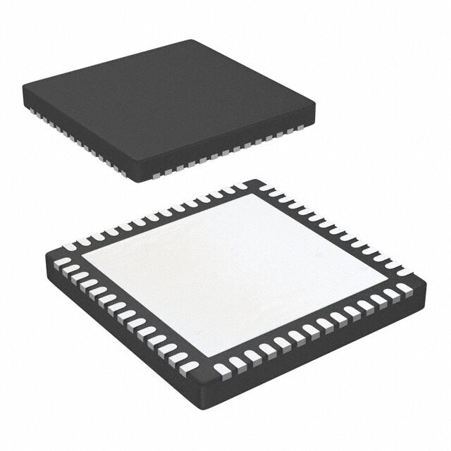
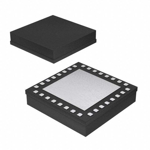
ICGOO电子元器件商城为您提供MAX2150ETI+由Maxim设计生产,在icgoo商城现货销售,并且可以通过原厂、代理商等渠道进行代购。 MAX2150ETI+价格参考¥78.86-¥78.86。MaximMAX2150ETI+封装/规格:RF 调制器, RF Modulator IC 700MHz ~ 2.3GHz 28-WFQFN Exposed Pad。您可以下载MAX2150ETI+参考资料、Datasheet数据手册功能说明书,资料中有MAX2150ETI+ 详细功能的应用电路图电压和使用方法及教程。
MAX2150ETI+ 是 Maxim Integrated(现为 Analog Devices, Inc.)生产的一款 RF 调制器,主要用于无线通信系统中的射频信号处理。它是一款高度集成的零中频 (Zero-IF) 调制器,适用于多种应用场景。

 主要应用场景:

1. 无线基础设施:
   - MAX2150ETI+ 广泛应用于基站、小基站和中继站等无线通信基础设施中。它能够将基带信号调制成射频信号,支持 GSM、CDMA、WCDMA 等多种通信标准,特别适合于 3G 和 4G 网络的部署。

2. 软件定义无线电 (SDR):
   - 在 SDR 系统中,MAX2150ETI+ 可以灵活地配置为不同的调制模式,适应多种无线协议。它的高集成度和低功耗特性使其成为便携式和嵌入式 SDR 设备的理想选择。

3. 点对点和点对多点通信:
   - 该器件适用于微波链路、Wi-Fi 扩展、无线回传等场景。其宽频带支持和高线性度确保了在长距离通信中的稳定性和可靠性。

4. 工业无线通信:
   - 在工业自动化和物联网 (IoT) 领域,MAX2150ETI+ 可用于构建可靠的无线传感网络和远程控制设备。它能够在复杂的电磁环境中提供稳定的射频传输性能。

5. 军事和航空航天:
   - 对于需要高可靠性和高性能的军事通信系统,MAX2150ETI+ 提供了卓越的抗干扰能力和精确的信号调制能力。它还可以用于卫星通信、无人机控制等应用。

6. 测试与测量设备:
   - 在射频测试仪器中,MAX2150ETI+ 可作为信号源或调制器,帮助工程师进行各种无线通信系统的测试和验证。

 特点和优势:

- 高集成度:内置多个功能模块,减少了外部元件数量,简化了设计。
- 低功耗:适用于电池供电的便携式设备,延长工作时间。
- 宽频带支持:覆盖从几百 MHz 到几 GHz 的频率范围,满足不同应用需求。
- 优异的线性度和噪声性能:确保高质量的信号传输,减少失真和干扰。

总之,MAX2150ETI+ 凭借其高性能和灵活性,成为众多无线通信系统中不可或缺的关键组件。
| 参数 | 数值 |
| 产品目录 | |
| 描述 | IC MODULATOR I/Q WIDE 28TQFN调节器/解调器 I/Q Mod w/Sig Delt Fractional-N Synth |
| DevelopmentKit | MAX2150EVKIT+ |
| 产品分类 | |
| LO频率 | 700MHz ~ 2.3GHz |
| 品牌 | Maxim Integrated |
| 产品手册 | |
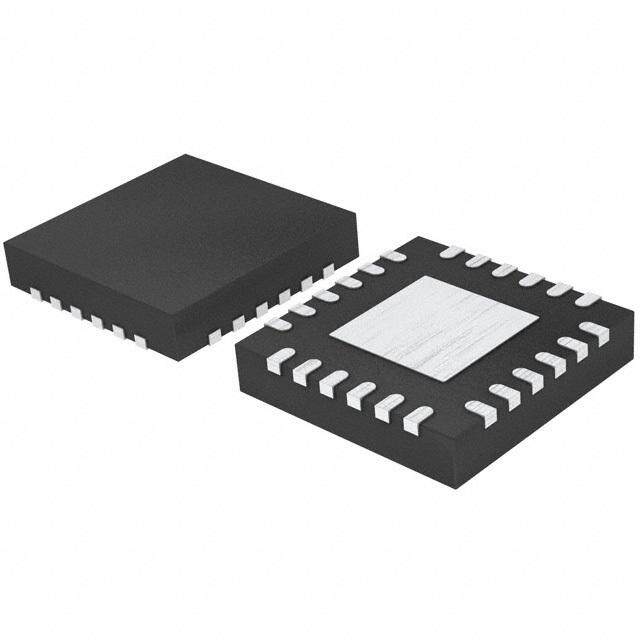
| 产品图片 |
|
| rohs | 符合RoHS无铅 / 符合限制有害物质指令(RoHS)规范要求 |
| 产品系列 | RF集成电路,调节器/解调器,Maxim Integrated MAX2150ETI+- |
| 数据手册 | |
| P1dB | 1dBm |
| 产品型号 | MAX2150ETI+ |
| RF频率 | 700MHz ~ 2.3GHz |
| 产品培训模块 | http://www.digikey.cn/PTM/IndividualPTM.page?site=cn&lang=zhs&ptm=25703http://www.digikey.cn/PTM/IndividualPTM.page?site=cn&lang=zhs&ptm=25705 |
| 产品种类 | 调节器/解调器 |
| 功能 | 调制器 |
| 包装 | 管件 |
| 商标 | Maxim Integrated |
| 安装风格 | SMD/SMT |
| 封装 | Tube |
| 封装/外壳 | 28-WFQFN 裸露焊盘 |
| 封装/箱体 | TQFN-28 |
| 工作温度范围 | - 40 C to + 85 C |
| 工作电压 | 2.7 V to 3.6 V |
| 工作电源电压 | 2.7 V to 3.6 V |
| 工厂包装数量 | 60 |
| 应用说明 | |
| 接口类型 | 3-Wire |
| 最大功率耗散 | 2 W |
| 最大工作温度 | + 85 C |
| 最小工作温度 | - 40 C |
| 本底噪声 | -148dBm/Hz |
| 标准包装 | 1 |
| 测试频率 | 1.75GHz |
| 电压-电源 | 2.7 V ~ 3.6 V |
| 电流-电源 | 46mA |
| 电源电流 | 107 mA |
| 系列 | MAX2150 |
| 调制类型 | Quadrature |
| 输出功率 | - 60 dBm |
| 零件号别名 | MAX2150 |


- 商务部:美国ITC正式对集成电路等产品启动337调查
- 曝三星4nm工艺存在良率问题 高通将骁龙8 Gen1或转产台积电
- 太阳诱电将投资9.5亿元在常州建新厂生产MLCC 预计2023年完工
- 英特尔发布欧洲新工厂建设计划 深化IDM 2.0 战略
- 台积电先进制程称霸业界 有大客户加持明年业绩稳了
- 达到5530亿美元!SIA预计今年全球半导体销售额将创下新高
- 英特尔拟将自动驾驶子公司Mobileye上市 估值或超500亿美元
- 三星加码芯片和SET,合并消费电子和移动部门,撤换高东真等 CEO
- 三星电子宣布重大人事变动 还合并消费电子和移动部门
- 海关总署:前11个月进口集成电路产品价值2.52万亿元 增长14.8%


PDF Datasheet 数据手册内容提取
19-2389; Rev 4; 6/08 Wideband I/Q Modulator with Sigma-Delta Fractional-N Synthesizer General Description Features M The MAX2150 is a complete wideband direct upconver- ♦ Single Voltage Supply (2.7V to 3.6V) A sion quadrature modulator IC incorporating a 28-bit ♦ 75MHz 3dB I/Q Input Bandwidth X sigma-delta fractional-N synthesizer. The device is tar- geted for applications in the 700MHz to 2300MHz fre- ♦ Wideband 50ΩRF Output: 700MHz to 2300MHz 2 quency range. ♦ Ultra-Fine Frequency Resolution: 100mHz 1 The super-high-resolution sigma-delta fractional-N syn- 5 ♦ High Reference Frequency for Fast-Switching thesizer is capable of better than 50mHz resolution 0 Applications when used with a 10MHz reference. Other features: fully differential I/Q modulation inputs, an internal LO ♦ Ultra-Low Phase Noise buffer, and a 50Ωwideband output driver amplifier. ♦ Low Spurious and Reference Emissions A standard 3-wire interface is provided for synthesizer ♦ -1dBm RMS Output Power programming and overall device configuration. An on- chip low-noise crystal oscillator amplifier is also includ- ♦ 60dB RF Muting Control ed and can be configured as a buffer when an external ♦ 34dBc Typical Carrier Suppression reference oscillator is used. ♦ 34dBc Typical Sideband Suppression The device typically achieves 34dBc of carrier and side- band suppression at a -1dBm output level. The wide- ♦ Software- and Hardware-Controlled Shutdown band, internally matched RF output can also Modes be disabled while the synthesizer and 3-wire bus remain powered up for continuous programming. Ordering Information The device consumes 72mA from a single +3.0V sup- ply and is packaged in an ultra-compact 28-pin QFN PART TEMP RANGE PIN-PACKAGE package (5mm ✕5mm) with an exposed pad. MAX2150ETI -40°C to +85°C 28 TQFN-EP* Applications MAX2150ETI+ -40°C to +85°C 28 TQFN-EP* *EP = Exposed paddle. Wireless Broadband +Denotes lead-free package. Satellite Uplink Pin Configuration/ LMDS Functional Diagram Wireless Base Station VCC_RF I+ I- Q+ Q- BUFENBUFOUT 28 27 26 25 24 23 22 TXEN 1 21 LO+ VCC_PA 2 20 LO- RFOUT 3 0 90 19 VCC_LO N.C. 4 18 VCC_D N.C. 5 MAX2150 1/N 17 VCC_A LOCK 6 ∑ Δ – MOD PFD CHP 16 CHP 1/R VCC_SD 7 PROGRAMMING 15 VCC_CHP AND CONTROL 8 9 10 11 12 13 14 CLK DATA EN SHDN SYNEN OSCIN VCC_XTAL QFN ________________________________________________________________Maxim Integrated Products 1 For pricing, delivery, and ordering information,please contact Maxim Directat 1-888-629-4642, or visit Maxim’s website at www.maxim-ic.com.
Wideband I/Q Modulator with Sigma-Delta Fractional-N Synthesizer 0 ABSOLUTE MAXIMUM RATINGS 5 VCCto GND...........................................................-0.3V to +6.0V Continuous Power Dissipation 1 RF Signals: LO+, LO-, OSCIN........................................+10dBm 28-Pin TQFN (TA = +70°C)..................................................2W 2 I+ to I-, Q+ to Q-.......................................................................2V (derate 28.5mW/°C above +70°C) LO+, LO-, I+, I-, Q+, Q-, BUFEN, TXEN, CLK, DATA, Operating Temperature Range...........................-40°C to +85°C X EN, SYNEN, OSCIN, OSCOUT, BUFOUT, CHP, Junction Temperature Range..........................................+150°C A SHDN,LOCK, VCC_CP to GND..............-0.3V to (VCC + 0.3V) Storage Temperature.........................................-65°C to +150°C Digital Input Current.........................................................±10mA Lead Temperature (soldering 10s)..................................+300°C M Short-Circuit Duration RFOUT, BUFOUT, OSCOUT, Lock, CHP...........................................................................10s Stresses beyond those listed under “Absolute Maximum Ratings” may cause permanent damage to the device. These are stress ratings only, and functional operation of the device at these or any other conditions beyond those indicated in the operational sections of the specifications is not implied. Exposure to absolute maximum rating conditions for extended periods may affect device reliability. CAUTION! ESD SENSITIVE DEVICE DC ELECTRICAL CHARACTERISTICS (MAX2150 EV kit. VCC= +2.7V to +3.6V, GND = 0V, SHDN= PLLEN = TXEN = high, BUFEN= low. No AC input signals. RFOUT and BUFOUT output ports are terminated in 50Ω. TA= -40°C to +85°C. Typical values are at VCC= +3V, TA= +25°C, unless otherwise noted.) (Note 1) PARAMETER CONDITIONS MIN TYP MAX UNITS SUPPLY Supply Voltage 2.7 3 3.6 V TX mode, SHDN = PLLEN = TXEN = high 72 107 BUFEN = low SYNTH mode, SHDN = PLLEN = high, TXEN = Supply Current 25 38 mA BUFEN = low MOD mode, SHDN = TXEN = high, SYNEN = 46 69 BUFEN = low LO Buffer Supply Current Additional current in all modes for BUFEN = high 3.3 5.5 mA HW_SHDN mode, SHDN = low 0.3 600 Shutdown Supply Current µA SW_SHDN mode, PWDN bit at logic low 35 600 CONTROL INPUT/OUTPUTS (SHDN, TXEN, SYNEN, BUFEN) Input Logic High 2 V Input Logic Low 0.5 V Input Logic High Current 1 µA Input Logic Low Current -1 µA Lock Detect High (Locked) 2 V Lock De tect Low ( Un l ocked ) 0.5 V Power-Up Time MOD mode 25 µs Power-Down Time MOD mode 1 µs 3-WIRE CONTROL INPUT (CLK, DATA, EN) VCC - Input Logic High V 0.5 Input Logic Low 0.5 V Input Logic High Current 1 µA Input Logic Low Current -1 µA 2 _______________________________________________________________________________________
Wideband I/Q Modulator with Sigma-Delta Fractional-N Synthesizer AC ELECTRICAL CHARACTERISTICS M (MAX2150 EV kit. VCC= +2.7V to +3.6V, SHDN= PLLEN = TXEN = high, BUFEN =low. Input I/Q signals: FI/Q = 500kHz, VI/Q = 1VP-P. A I+, Q+ single-ended input, driven from AC-coupled source. I-, Q- single-ended inputs are AC-coupled to GND. RFOUT and BUFOUT output ports are terminated in 50Ωloads. fLO=1750MHz, PLO= -10dBm, typical values are at VCC= +3V, TA= +25°C, unless other- X wise noted.) (Note 1) 2 PARAMETER CONDITIONS MIN TYP MAX UNITS 1 MODULATION INPUT 5 BW (-1dB) 26 0 I/Q Input Bandwidth MHz BW (-3dB) 75 Assumes a sine-wave input to achieve the RFOUT output I/Q Differential Input Level 1 VP-P power specified below I/Q DC Input Resistance 200 kΩ I/Q Common-Mode Input Range (Note 2) 1.5 1.6 1.7 V RF OUTPUT Frequency Range 700 2300 MHz TXEN = high, fRF = 1750MHz -7 -1 Output Power dBm TXEN = low, fRF = 1750MHz -60 Output 1dB Compression Point 1 dBm Output IP3 14 dBm Carrier Suppression fRF = 1750MHz 34 dBc Sideband Suppression fLO - fI/Q, fRF = 1750MHz 25 34 dBc RF Output Noise Floor fOFFSET > 40MHz (Note 2) -148 -143 dBm/Hz Output Return Loss (Note 3) -9 dB LO INPUT/OUTPUT Frequency Range 700 2300 MHz LO Input Power (Note 2) -12 -10 -7 dBm LO Input Return Loss fLO =2000MHz -15 dB LO Buffer Output Level BUFEN = high (Note 2) -14 -9.5 dBm SIGMA-DELTA FRACTIONAL-N SYNTHESIZER SYSTEM REQUIREMENTS Frequency Range (Note 2) 700 2300 MHz Phase-Detector Input-Referred fCOMP = fREF = 20MHz, CP0 = CP1 = CPX = 1 (Note 4) -138 dBc/Hz Phase Noise Floor fLO = 1740.005MHz, fCOMP = fREF = 20MHz, CP0 = CP1 In-Loop Spurious Emissions -40 dBc = CPX = 1 (Note 5) MAIN DIVIDER AND PHASE DETECTOR fCOMP/ Minimum Fractional-N Step Size 228 Phase-Detector Comparison 20 30 MHz Frequency Maximum N Division 251 Minimum N Division 35 _______________________________________________________________________________________ 3
Wideband I/Q Modulator with Sigma-Delta Fractional-N Synthesizer 0 AC ELECTRICAL CHARACTERISTICS (continued) 5 (MAX2150 EV kit. VCC= +2.7V to +3.6V, SHDN= PLLEN = TXEN = high, BUFEN = low. Input I/Q signals: FI/Q = 500kHz, VI/Q = 1VP-P. 1 I+, Q+ single-ended input, driven from AC-coupled source. I-, Q- single-ended inputs are AC-coupled to GND. RFOUT and BUFOUT 2 output ports are terminated in 50Ωloads. fLO=1750MHz, PLO= -10dBm, typical values are at VCC= +3V, TA= +25°C, unless other- wise noted.) (Note 1) X PARAMETER CONDITIONS MIN TYP MAX UNITS A REFERENCE OSCILLATOR AND DIVIDER M Input Frequency Range 10 50 MHz AC-Coupled Input Sensitivity AC-coupled, single ended (Note 2) 0.4 2.3 VP-P Reference Division Ratio (Notes 2, 6) 1 4 CHARGE-PUMP OUTPUT CPX = 0 0.12 0.17 0.22 CP1, CP0 = 00 CPX = 1 0.23 0.34 0.44 CPX = 0 0.23 0.35 0.46 CP1, CP0 = 01 CPX = 1 0.47 0.67 0.88 Charge-Pump Current (Note 7) mA CPX = 0 0.36 0.52 0.68 CP1, CP0 = 10 CPX = 1 0.70 1.00 1.30 CPX = 0 0.48 0.69 0.90 CP1, CP0 = 11 CPX = 1 0.91 1.31 1.70 Charge-Pump Voltage VCC - Sink/source currents match within ±5% 0.5 V Compliance 0.5 Note 1: Parameters are guaranteed by production testing at +25°C and +85°C. Minimum and maximum values over the tempera- ture and supply voltage range are guaranteed by design and characterization. Note 2: Guaranteed by design and characterization. Note 3: Measured with MAX2150 EV kit. Note 4: Measured with an on-chip crystal oscillator. Note 5: In-loop spurious emissions occur when synthesizing a frequency at an integer multiple of the comparison frequency with fractional offset within the PLL loop BW. Note 6: If an on-chip oscillator is used, a fundamental tone crystal is needed. Note 7: Minimum and maximum values at CPX = 1 are guaranteed by production testing. Values at CPX = 0 are guaranteed by design and characterization. 4 _______________________________________________________________________________________
Wideband I/Q Modulator with Sigma-Delta Fractional-N Synthesizer Typical Operating Characteristics M (MAX2150 EV kit. VCC= +3V, SHDN= PLLEN = TXEN = high, BUFEN = low. Input I/Q signals: FI/Q= 500kHz, VI/Q= 1VP-P. I+, Q+ sin- A gle-ended input, driven from AC-coupled source. I-, Q- single-ended inputs are AC-coupled to GND. RFOUT and BUFOUT output ports are terminated in 50Ωloads. fLO=1750MHz, PLO= -10dBm, TA= +25°C, unless otherwise noted.) X 2 SUPPLY CURRENT MODULATION OUTPUT POWER MODULATION OUTPUT POWER 1 vs. SUPPLY VOLTAGE vs. FREQUENCY vs. FREQUENCY 5 mA) 18000 TX MODE ++8255°°CC MAX2150 toc01 WER (dBm) 024 TXEN = HIGH -40°C MAX2150 toc02 WER (dBm) --5585 TXEN = L-O4W0°C MAX2150 toc03 0 SUPPLY CURRENT ( 4600 -40°C ULATION OUTPUT PO ----8642 +85°C +25°C ULATION OUTPUT PO --6641 ++8255°°CC 20 OD OD -67 M -10 M 0 -12 -70 2.7 3.0 3.3 3.6 700 1100 1500 1900 2300 700 1100 1500 1900 2300 SUPPLY VOLTAGE (V) FREQUENCY (MHz) FREQUENCY (MHz) CARRIER AND SIDEBAND MODULATOR OUTPUT POWER OUTPUT POWER vs. LO POWER SUPPRESSIONS vs. LO POWER vs. I/Q INPUT LEVEL OUTPUT POWER (dBm) ---------111111111.........876543210 MAX2150 toc04 RIER AND SIDEBAND SUPPRESSIONS (dB) 333333345678 SIDEBANCDA RSRUIPERP RSEUSPSPIORNESSION MAX2150 toc05 MODULATOR OUTPUT POWER (dBm) ---211--8404062 -40°C +85°C +25°C MAX2150 toc06 -1.9 AR C -2.0 32 -24 7 8 9 10 11 12 7 8 9 10 11 12 0 200 400 600 800 1000 1200 1400 LO POWER (dBm) LO POWER (dBm) I/Q INPUT LEVEL (mV) _______________________________________________________________________________________ 5
Wideband I/Q Modulator with Sigma-Delta Fractional-N Synthesizer 0 Typical Operating Characteristics (continued) 5 (MAX2150 EV kit. VCC= +3V, SHDN= PLLEN = TXEN = high, BUFEN = low. Input I/Q signals: FI/Q= 500kHz, VI/Q= 1VP-P. I+, Q+ 1 single-ended input, driven from AC-coupled source. I-, Q- single-ended inputs are AC-coupled to GND. RFOUT and BUFOUT output 2 ports are terminated in 50Ωloads. fLO=1750MHz, PLO= -10dBm, TA= +25°C, unless otherwise noted.) X LO PORT INPUT RETURN LOSS A MODULATOR OUTPUT IP3 vs. VCC MODULATOR OUTPUT P1dB vs. VCC vs. FREQUENCY MMODULATOR OUTPUT IP3 (dBm) 111111123456 ++-428055°°°CCC MAX2150 toc07 MODULATOR OUTPUT P1dB (dBm) 011223......0505050 ++-428055°°°CCC MAX2150 toc08 LO PORT RETURN LOSS (dB) ----2211-505050 MAX2150 toc09 -0.5 10 -1.0 -30 2.7 3.0 3.3 3.6 2.7 3.0 3.3 3.6 700 1100 1500 1900 2300 VCC (V) VCC (V) FREQUENCY (MHz) BUFOUT PORT RETURN LOSS LO BUFFER OUTPUT POWER LO BUFFER OUTPUT POWER vs. FREQUENCY vs. FREQUENCY vs. FREQUENCY LOSS (dB) -1-050 MAX2150 toc10 WER (dBm) ----7654 BUFEN = HIGH +85°C MAX2150 toc11 WER (dBm) --4430 BUFEN = LOW MAX2150 toc12 BUFOUT PORT RETURN ---221505 LO BUFFER OUTPUT PO ---111--21098 +25°C -40°C LO BUFFER OUTPUT PO ---544296 +85°C +25-°4C0°C -13 -30 -14 -55 700 1100 1500 1900 2300 700 1100 1500 1900 2300 700 1100 1500 1900 2300 FREQUENCY (MHz) FREQUENCY (MHz) FREQUENCY (MHz) 6 _______________________________________________________________________________________
Wideband I/Q Modulator with Sigma-Delta Fractional-N Synthesizer Typical Operating Characteristics (continued) M (MAX2150 EV kit. VCC= +3V, SHDN= PLLEN = TXEN = high, BUFEN = low. Input I/Q signals: FI/Q= 500kHz, VI/Q= 1VP-P. I+, Q+ A single-ended input, driven from AC-coupled source. I-, Q- single-ended inputs are AC-coupled to GND. RFOUT and BUFOUT output ports are terminated in 50Ωloads. fLO=1750MHz, PLO= -10dBm, TA= +25°C, unless otherwise noted.) X 2 OSCIN PORT SENSITIVITY 1 (SYNTHESIZER) vs. FREQUENCY OSCIN IMPEDANCE vs. FREQUENCY 5 OSCIN PORT SENSITIVITY (V) 23456 +25°+C85°C ++-428055°°°CCC MAX2150 toc13 00000.....2345600000 ΩOSCIN PORT IMPEDANCE ()--------8765432100000000000000000 REAL IMAGINARY MAX2150 toc14 0 1 0.10 -40°C -900 0 0 -1000 10 15 20 25 30 35 40 45 50 10 15 20 25 30 35 40 45 50 FREQUENCY (MHz) FREQUENCY (MHz) SYNTHESIZER PHASE NOISE I/Q MODULATOR OUTPUT SPURS --21000 -8.5dBm MAX2150 toc15 --21000 SUCP-PA3RR4EdRSBIEScRIONSIDMEABXA21N50D toc16 SUPPRESSION -30 -30 1 AVG -36dBc -40 -40 -50 -50 -60 -60 N/C = -99dBc/Hz -70 -70 -80 -80 -90 -90 -100 -100 CENTER = 1.75MHz SPAN = 20kHz CENTER = 1.75 GHz SPAN = 2 MHz _______________________________________________________________________________________ 7
Wideband I/Q Modulator with Sigma-Delta Fractional-N Synthesizer 0 Pin Description 5 1 PIN NAME FUNCTION 2 Modulator Enable Input. Set TXEN low to inhibit the RF and modulator circuits. This mode can be used 1 TXEN X for quiet frequency synthesis. A Supply Voltage Input for RFOUT Output Driver Circuits. Bypass as close to the pin as possible. The 2 VCC_PA M bypass capacitor should not share ground vias with other branches. Modulator RF Output. This is a wideband, internally matched 50Ω output. A DC-blocking capacitor is 3 RFOUT required. 4, 5 N.C. Do Not Connect. (These pins must be left floating.) 6 LOCK Lock Status of the PLL. A static logic-level high indicates that the PLL is in the locked condition. Supply Voltage Input for Sigma-Delta Modulator Circuits. Bypass as close to the pin as possible. The 7 VCC_SD bypass capacitor should not share ground vias with other branches. CLK, DATA, Input Pins from 3-Wire Serial Bus. An RC lowpass filter on each of these pins can be used to reduce 8, 9, 10 EN digital noise. Shutdown Control. Set SHDN low to disable all internal circuits for lowest power consumption. An RC 11 SHDN lowpass filter can be used to reduce digital noise. Synthesizer Enable Input. Set SYNTH low to disable the internal frequency synthesizer. An RC lowpass 12 SYNEN filter can be used to reduce digital noise. Reference Oscillator Input. Connect a parallel, resonant, fundamental-tone crystal between this pin and 13 OSCIN ground to facilitate a crystal oscillator circuit. For applications with an external reference oscillator, the OSCIN input can be driven through a large-value series capacitor. Supply Voltage Input for Crystal Oscillator. Bypass as close to the pin as possible. The bypass capacitor 14 VCC_XTAL should not share ground vias with other branches. Supply Voltage Input for Charge Pump. Bypass as close to the pin as possible. The bypass capacitor 15 VCC_CHP should not share ground vias with other branches. High-Impedance Charge-Pump Output. Connect to the tune input of the VCO through the PLL loop filter. 16 CHP Keep the line from this pin to the tune input as short as possible to prevent spurious pickup, and connect the loop filter as close to the tune input as possible. Supply Voltage Input for PLL. Bypass as close to the pin as possible. The bypass capacitor should not 17 VCC_A share ground vias with other branches. Supply Voltage Input for PLL. Bypass as close to the pin as possible. The bypass capacitor should not 18 VCC_D share ground vias with other branches. Supply Voltage Input for Internal LO Circuits. Bypass as close to the pin as possible. The bypass 19 VCC_LO capacitor should not share ground vias with other branches. Differential Local-Oscillator Input. These inputs require DC-blocking capacitors. The LO can be applied 20, 21 LO-, LO+ with a single-ended input to the LO+/LO- pin. In this mode, the other pin should be AC-grounded. 22 BUFOUT Buffered LO Output. Internally matched to 50Ω, requires a DC-blocking capacitor. LO Output Buffer Amplifier Enable. Set BUFEN high to enable the on-chip output LO buffer for driving 23 BUFEN external circuits. An RC lowpass filter can be used to reduce digital noise. Differential Q-Channel Baseband Inputs to the Modulator. These pins connect directly to the bases of 24, 25 Q-, Q+ a differential pair and require an external common-mode bias voltage of 1.6V. 8 _______________________________________________________________________________________
Wideband I/Q Modulator with Sigma-Delta Fractional-N Synthesizer Pin Description (continued) M PIN NAME FUNCTION A Differential I-Channel Baseband Inputs to the Modulator. These pins connect directly to the bases of a X 26, 27 I-, I+ differential pair and require an external common-mode bias voltage of 1.6V. 2 Supply Voltage Input for RF Circuits. Bypass as close to pin as possible. The bypass capacitor should 1 28 VCC_RF not share ground vias with other branches. 5 — Exposed pad Ground 0 Detailed Description The modulator can be shut down with both hardware (pin 1) and software (TE bit). This mode is useful for Internally, the MAX2150 includes a broadband I/Q quiet synthesizer programming or to mute the RF out- modulator, internally matched broadband output driver put signal. The hardware pin and software bits must be amplifier, fine-resolution fractional-N frequency synthe- set to logic-1 to enable the modulator. If the hardware sizer, an LO buffer amplifier, and an on-chip low-noise pin or software bit is set to logic-0, or if both are set to crystal oscillator circuit. logic-0, the modulator is disabled. A simple 3-wire interface is provided for synthesizer programming and device configuration and control. LO Buffer Amplifier Independent hardware and software power-down con- The broadband buffer amplifier output is internally trol of the I/Q modulator, frequency synthesizer, and LO matched and requires a DC-blocking capacitor to iso- buffer amplifier is provided, as well as the ability to shut late on-chip bias voltages. Power-down of the LO buffer down the entire chip. can be controlled by both BUFEN (pin 23), as well as BUFEN by software by setting the BUFEN (BE) bit I/Q Modulator through the 3-wire interface. The hardware pin and the The MAX2150 modulator is composed of a pair of software bit must be a logic-1 to enable the buffer. If matched double-balanced mixers, a broadband pas- the hardware or software bit is set to logic-0, the LO sive LO quadrature generator, and a summing amplifi- buffer is disabled. er. The mixers accept differential I/Q baseband signals that directly modulate the internal 0° and 90° LO sig- Frequency Synthesizer nals applied to the I/Q mixers. An external LO source The MAX2150 features an internal 28-bit sigma-delta drives an internal LO quadrature generator that shifts frequency synthesizer. This architecture enables the the phase of the LO signal applied to the Q mixer by use of very high (30MHz) comparison frequencies, 90° relative to the LO signal applied to the I-channel which significantly reduces the in-loop phase noise as mixer. The modulated output of the I/Q mixers is a result of reduced division ratios. The high comparison summed together, and the undesired sideband is sup- frequency also allows significantly increased PLL pressed. bandwidths for very fast switching speed applications. The I+, I-, Q+, and Q- input ports feature high-linearity Divider Programming buffer amplifiers with a typical -3dB bandwidth of The MAX2150 frequency programming is determined 75MHz and accept differential input voltages up to as follows. The overall division ratio (D) has an integer 1VP-P. The ports require external biasing and have an value (N), as well as a fractional component (F): input common-mode requirement of 1.6V. For single- D = N.F = N +F / 228 ended operation, bypass the I and Q ports to ground. See the Typical Application Circuitfor recommended The N and F values are encoded as straight binary component values. numbers. Determination of these values is illustrated by the following example: The broadband output driver amplifier is matched on chip across the entire operating frequency range and FLO= 1721.125MHz, FCOMP= 20MHz requires an output DC-blocking capacitor. For optimum Then: performance, the output match can be improved with D = 1721.125 / 20 = 86.05625 simple L-section and/or PI-section matching networks. Always ensure that DC blocking is provided, because Therefore: internal bias voltages are present at this output. N = 86 and F = 0.05625 x 228= 15,099,494 _______________________________________________________________________________________ 9
Wideband I/Q Modulator with Sigma-Delta Fractional-N Synthesizer 0 Converting each to binary representation results in the Fractional Spurs 5 following: When synthesizing a frequency that is an integer multi- 1 N register = 86 = 0101,0110 ple of the reference divider and having a fractional off- set with a value less than the PLL filter bandwidth, 2 F register value = fractional spurs can be observed at a typical level of X 0000,1110,0110,0110,0110,0110,0110 -40dBc. For example, to synthesize 1640.005MHz A The F-register value is then split between an upper 14 when using a 20MHz reference and a PLL bandwidth of bits and a lower 14 bits as follows: 25kHz, spurious products offset from the LO by 5kHz M can be observed. The 1640MHz is an integer multiple Upper 14 bits + address 00 = 0000,1110,0110,0100 of 20MHz, and the fractional offset of 5kHz is within the Lower 14 bits + address 01 = 1001,1001,1001,1001 PLL bandwidth. Synthesizer Shutdown It is possible to avoid the above-mentioned spurious The synthesizer can be disabled by setting SYNEN (pin products by using two reference oscillators with slightly 12) to a logic low. This mode is useful when an external offset frequencies or by using a higher reference fre- frequency synthesizer is employed. quency and changing the comparison frequency of the reference divider. Applications Information Crystal Oscillator Serial Interface and Register Definition The MAX2150 includes a simple-to-use on-chip low- 3-Wire Interface and Registers noise reference oscillator circuit. The oscillator is The MAX2150 is programmed through a simple formed by connecting a fundamental mode parallel res- 3-wire (CLK, DATA, EN) interface. The programming onant crystal from OSCIN to ground. The oscillator cir- data is contained within 16-bit words loaded into four cuit is useful from 10MHz to 50MHz. unique address locations. Each location contains pro- The phase noise of the MAX2150 can be improved by gramming information for setting operational modes using a precision high-frequency external reference and device configuration. Two words (address 00, 01) oscillator (TCXO). The external oscillator is connected control the fractional divide number in the sigma-delta through a DC-blocking capacitor directly to the OSCIN synthesizer. The third word (address 10) sets the inte- pin. ger divide value, reference divide value, charge-pump current, and charge-pump compensation DAC settings. Layout Considerations The fourth and final word (address 11) contains various A properly designed PC board is an essential part of device configuration registers and test registers, as any RF circuit. A ground plane is essential. Keep RF well as additional charge-pump compensation regis- signal lines as short as possible to reduce losses, radi- ters. See Tables 1 through 11 for details. ation, and inductance. The exposed pad on the under- side of the MAX2150 must be adequately grounded by 3-Wire Interface Timing Diagram ensuring that the exposed paddle of the device pack- Figure 1 shows the programming logic. The 16-bit shift age is soldered evenly to the board ground plane. Use register is programmed by clocking in data at the rising multiple, low-inductance vias to ground the exposed edge of CLK. Pulling enable low allows data to be paddle. clocked into the shift register; pulling enable high loads the register addressed. DATA B19 (MSB) B18 B0 A3 A1 A0 (LSB) tCS > 50ns tCH > 10ns tCWH > 50ns CLK tES > 50ns tCWL tCWL > 50ns tEW > 50ns tCS tCH tCWH tES EN tEW Figure 1. 3-Wire Interface Timing Diagram 10 ______________________________________________________________________________________
Wideband I/Q Modulator with Sigma-Delta Fractional-N Synthesizer Table 1. Register Tables M MSB SHIFT REGISTER DATA LSB ADDRESS A Upper (MSBs) Fractional Divider Value (F) 14 Bits (Default = 8192, 10000000000000) Address X 27 26 25 24 23 22 21 20 19 18 17 16 15 14 0 0 2 Lower (LSBs) Fractional Divider Value (F)14 Bits (Default 0 DEC, 00000000000000 Address 1 13 12 11 10 9 8 7 6 5 4 3 2 1 0 0 1 5 R Divider CP Bleed CP Current Integer Divide Value (N) 8 Bits 0 Address Default = 00 Default = 00 Default = 11 Default = 177 DEC R1 R0 LIN1 LIN0 CP1 CP0 7 6 5 4 3 2 1 0 1 0 Reset Delay Test Registers 6 Bits Control Register 6 Bits Address Default = 00 Default = 0 DEC Default = 15 DEC BL1 BL0 T5 T4 T3 T2 T1 T0 INT PD TE BE XX CPX 1 1 Table 2. Reference Divider R1 R0 REFERENCE DIVIDE VALUE 0 0 1 0 1 2 1 0 3 1 1 4 Table 3. Integer Divider-N* N7 N6 N5 N4 N3 N2 N1 N0 INTEGER DIVIDE VALUE 0 0 1 0 0 0 1 1 35 0 0 1 0 0 1 0 0 36 — — — — — — — — — 1 1 1 1 1 0 1 0 250 1 1 1 1 1 0 1 1 251 *N divider is limited to 35 < N < 251. Table 4. Fractional Divider-F (Upper 14 Bits) F27 F26 F25 F24 F23 F22 F21 F20 F19 F18 F17 F16 F15 F14 0 0 0 0 0 0 0 0 0 0 0 0 0 0 0 0 0 0 0 0 0 0 0 0 0 0 0 0 — — — — — — — — — — — — — — 1 1 1 1 1 1 1 1 1 1 1 1 1 1 Table 5. Fractional Divider-F (Lower 14 Bits) INTEGER DIVIDE F13 F12 F11 F10 F9 F8 F7 F6 F5 F4 F3 F2 F1 F0 VALUE 0 0 0 0 0 0 0 0 0 0 0 0 0 0 1 0 0 0 0 0 0 0 0 0 0 0 0 0 1 2 — — — — — — — — — — — — — — — 1 1 1 1 1 1 1 1 1 1 1 1 1 0 268435454 1 1 1 1 1 1 1 1 1 1 1 1 1 1 268435455 ______________________________________________________________________________________ 11
Wideband I/Q Modulator with Sigma-Delta Fractional-N Synthesizer 0 Table 6. Control Register 5 1 BIT PWR-UP BIT LOCATION BIT ID FUNCTION NAME STATE 0 = LSB 2 X A logic high doubles the charge pump current selected through registers CPX CP_MULT 1 0 CP1 and CP0. Logic low sets the charge-pump current to the value A selected by registers CP1 and CP0. M XX XX XX 1 Unused. BE BUFEN 1 2 High enables the VCO buffer. Low disables this output. Low enables SW_MUTE mode, which shuts down the RF circuits while TE TXEN 1 3 leaving the 3-wire interface, register, and PLL circuits active. Low enables register-based shutdown. This mode shuts down all circuits PD PWDN 0 4 except the 3-wire interface and internal registers. Logic high disables the sigma-delta modulator. Logic low enables the INT INT_MODE 0 5 sigma-delta modulator for normal operation. Table 7. Device Modes SOFTWARE CONTROL HW PINS MODE BITS DESCRIPTION SHDN TXEN SYNEN BUFEN PWDN TXEN BUFEN TX H H H H/L H H H/L All circuits active. Modulator circuits active. Synthesizer MOD H H L H/L H H H/L blocks disabled. Mode is used with external PLL circuit. Serial interface and synthesizer blocks active. RF and modulator blocks disabled. SYNTH H L H H/L H X H/L Mode is used to gate RF ON/OFF with external logic control. Serial interface and synthesizer blocks all active. Modulator blocks disabled. Mode is SW_MUTE H H H H/L H L H/L used to gate RF ON/OFF with software control. All circuits disabled. Lowest current mode HW_SHDN L X X X X X X of operation. Serial interface and registers active, all other circuits inactive regardless of the SW_SHDN H X X X L X X state of the HW pins with the exception of HW_SHDN. Power-Supply (VCC) Bypassing and share no common vias with any other ground con- Proper voltage-supply bypassing is essential to reduce nection. See the Typical Operating Circuitfor suggest- the spurious emissions mentioned above. It is recom- ed bypass component values. mended that each VCCpin be bypassed independently 12 ______________________________________________________________________________________
Wideband I/Q Modulator with Sigma-Delta Fractional-N Synthesizer Table 8. TXEN Pin and Software Bit Table 11. BUFEN Pin and Software Bit M Definitions Definitions A TXEN BUFEN X TX MODE BUF MODE PIN BIT PIN BIT 2 0 0 TX off 0 0 Buffer off 1 0 1 TX off 0 1 Buffer off 5 1 0 TX off 1 0 Buffer off 0 1 1 TX enabled 1 1 Buffer on Table 9. Charge-Pump Registers Chip Information CPX CP1 CP0 ICP (µA) TRANSISTORCOUNT: 16,321 0 0 0 170 0 0 1 350 0 1 0 520 0 1 1 690 Package Information 1 0 0 340 For the latest package outline information and land patterns, go 1 0 1 670 to www.maxim-ic.com/packages. 1 1 0 1000 1 1 1 1310 PACKAGE TYPE PACKAGE CODE DOCUMENT NO. 28 TQFN-EP T2855-3 21-0140 Table 10. Test Register Definition (Default 0 Dec)* TEST MODE T5 T4 T3 T2 T1 T0 TEST PIN Normal Operating 0 0 0 0 0 0 — Mode Charge Pump Forced to 0 0 0 0 0 1 CP Source Icp Charge Pump Forced to Sink 0 0 0 0 1 0 CP Icp Reference 0 1 0 0 0 0 Lock Divider Output Main Divider 0 1 1 0 0 0 Lock Output *All other logic states are undefined. ______________________________________________________________________________________ 13
Wideband I/Q Modulator with Sigma-Delta Fractional-N Synthesizer 0 Typical Operating Circuit 5 1 J1 J2 31-5239-52RFX 31-5239-52RFX 2 I IN Q QN X C50 C52 0.1μF 0.1μF A R31 R1 VCC 3.3kΩ OPEN M R29 3R.33k2Ω ORPE2N VCC OPEN BUFEN R4 DCIN 3R.33k3Ω ORPE3N OPEN C28 0.1μF 3R.33k4Ω 0.C1μ1F VCC VCC JJ67 C1μ25F C0.311μF 0.C1μ3F VCC 10C02pF CO5PENR01Ω2 CO6PEN J13BUFOUT GND 28 27 26 25 24 23 22 VCC_RF I+ I- Q+ Q- BUFEN BUFOUT 0C.13μ3F J14 1 TXEN LO+ 21 LO C7 C32 VCC OPEN 0.1μF C17 100pF 2 VCC_PA LO- 20 J15LOn C8 C20 22pF 0.1μF RFOUTJ8 R01Ω3 0C.11μ8F 3 RFOUT VCC_LO 19 VCC 1C001p2F 7 U2 V17C530RB03A5203F0U9J6I7/ C15 C16 1VT GNDVSW6 OPEN OPEN U1 VCC C4 J16 4 TEST2 MAX2150 VCC_D 18 100pF 2GND GND5 3 4 VCCGNDOUT VCC C10 8 J17 5 TEST1 VCC_A 17 C11 100pF 100pF VCC_VCO LOCK VCCJ20 6 LOCK CHP 16 C682020pF C10305pF C0.314μF J19 JJ151 VCCVCO VCCSD 7 VCC_SD VCC_CHP 15 VCC 10C09pF GND C1.207μF C10104pF CLK DATA EN SHDN SYNEN OSCIN VCC_XTAL 0C.11μ9F R24 R25 8 9 10 11 12 13 14 1.1kΩ 1.1kΩ EN JUMP_PAD SHDN R24253Ω C24 C26 C37VCC VCC 680pF 470pF 0.1μF C23 R35 .068μF OPEN C13 C21 VTUNE_OUT L1 100pF 0.1μF TUNEOUT OPEN C36 R18 LOCK CLK ENn DATA 0.1μF FILTVCC SHDNn TXEN SYNEN VCOSEL 0Ω Y1 C30 J10–1 J10–3 J10–5 J10–7 J10–9 J10–11 J10–13 J10–15 J10–17 J10–19 0.1μF J18 REFL In J10–2 J10–4 J10–6 J10–8 J10–10 J10–12 J10–14 J10–16 J10–18 J10–20 14 ______________________________________________________________________________________
Wideband I/Q Modulator with Sigma-Delta Fractional-N Synthesizer Revision History M A REVISION REVISION PAGES DESCRIPTION X NUMBER DATE CHANGED 2 4 6/08 Updated table in Package Information 13 1 5 0 Maxim cannot assume responsibility for use of any circuitry other than circuitry entirely embodied in a Maxim product. No circuit patent licenses are implied. Maxim reserves the right to change the circuitry and specifications without notice at any time. Maxim Integrated Products, 120 San Gabriel Drive, Sunnyvale, CA 94086 408-737-7600 ____________________15 © 2008 Maxim Integrated Products is a registered trademark of Maxim Integrated Products, Inc.
Mouser Electronics Authorized Distributor Click to View Pricing, Inventory, Delivery & Lifecycle Information: M axim Integrated: MAX2150ETI+ MAX2150ETI+T