ICGOO在线商城 > 射频/IF 和 RFID > RF 调制器 > HMC497LP4E
 Datasheet下载
- 型号: HMC497LP4E
- 制造商: Hittite
- 库位|库存: xxxx|xxxx
- 要求:
| 数量阶梯 | 香港交货 | 国内含税 |
| +xxxx | $xxxx | ¥xxxx |
查看当月历史价格
查看今年历史价格
HMC497LP4E产品简介:
ICGOO电子元器件商城为您提供HMC497LP4E由Hittite设计生产,在icgoo商城现货销售,并且可以通过原厂、代理商等渠道进行代购。 HMC497LP4E价格参考。HittiteHMC497LP4E封装/规格:RF 调制器, RF Modulator IC 100MHz ~ 4GHz 24-VFQFN Exposed Pad。您可以下载HMC497LP4E参考资料、Datasheet数据手册功能说明书,资料中有HMC497LP4E 详细功能的应用电路图电压和使用方法及教程。
HMC497LP4E 是由 Analog Devices Inc.(ADI)生产的一款 RF 调制器,属于高性能射频集成电路。该型号的主要应用场景包括:

1. 无线通信系统:HMC497LP4E 可用于蜂窝基站、中继站和其他无线基础设施设备中,提供高效的信号调制功能,支持多种通信标准。

2. 雷达与国防应用:在雷达系统和国防通信中,这款调制器可用于生成高精度的调制信号,满足复杂环境下的探测和通信需求。

3. 测试与测量设备:由于其卓越的线性度和带宽性能,HMC497LP4E 适用于高端信号发生器、频谱分析仪等测试仪器,帮助工程师精确评估射频信号特性。

4. 卫星通信:在卫星地面站或用户终端中,这款器件可以实现高质量的上变频调制,确保数据传输的可靠性和效率。

5. 宽带通信系统:支持宽带信号处理,适用于光纤到户(FTTH)、点对点微波链路以及其他需要高速数据传输的应用场景。

HMC497LP4E 的特点在于其宽带操作能力(高达 2 GHz),低插入损耗以及出色的线性度,使其成为上述领域中关键组件的理想选择。此外,其紧凑的封装形式(4x4 mm QFN)也便于集成到小型化设计中。
| 参数 | 数值 |
| 产品目录 | |
| 描述 | IC MODULATOR SIGE DIRECT 24-QFN |
| 产品分类 | |
| LO频率 | 100MHz ~ 4GHz |
| 品牌 | Hittite Microwave Corporation |
| 数据手册 | |
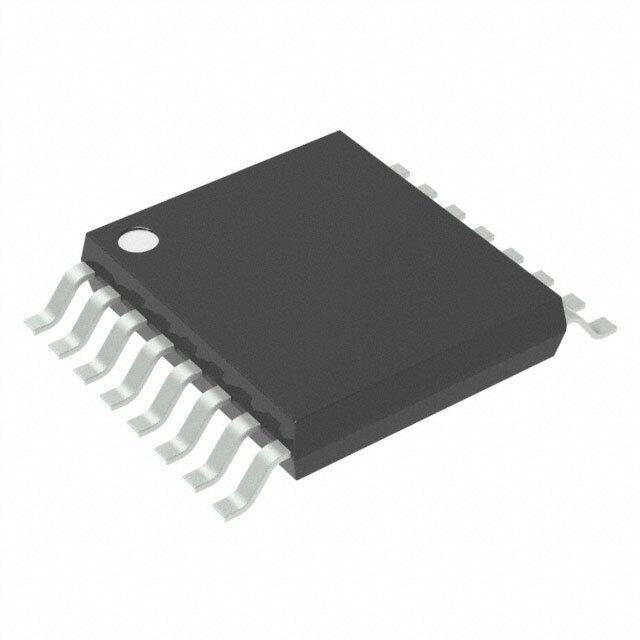
| 产品图片 |
|
| P1dB | 8dBm |
| 产品型号 | HMC497LP4E |
| RF频率 | 100MHz ~ 4GHz |
| rohs | 无铅 / 符合限制有害物质指令(RoHS)规范要求 |
| 产品系列 | - |
| 其它名称 | 1127-1431 |
| 功能 | 调制器 |
| 包装 | 散装 |
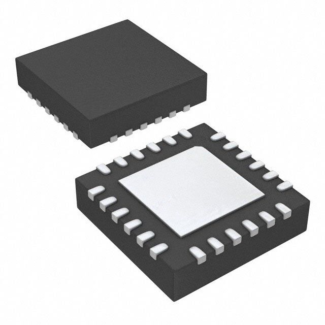
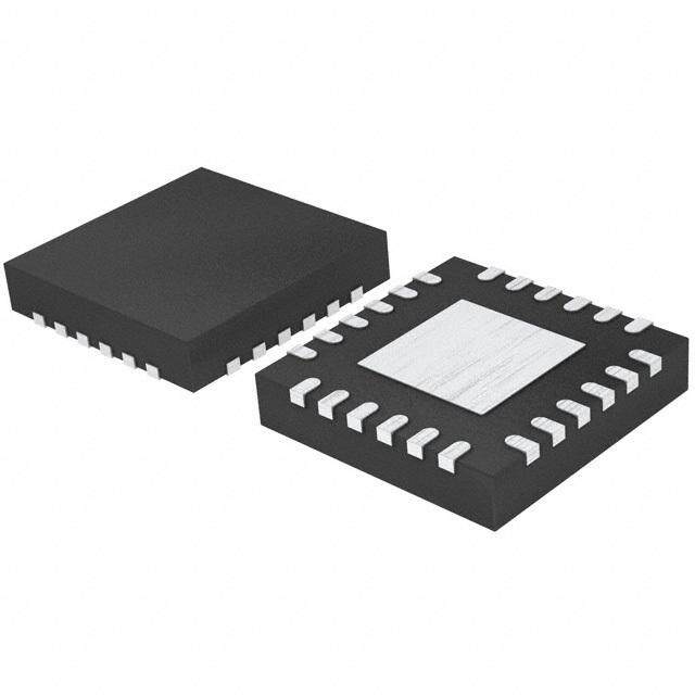
| 封装/外壳 | 24-VQFN 裸露焊盘 |
| 本底噪声 | -159dBm/Hz |
| 标准包装 | 100 |
| 测试频率 | 1.7GHz ~ 2.2GHz |
| 特色产品 | http://www.digikey.cn/product-highlights/zh/direct-iq-modulators/52283 |
| 电压-电源 | 4.5 V ~ 5.5 V |
| 电流-电源 | 168mA |
| 输出功率 | 5dBm |


- 商务部:美国ITC正式对集成电路等产品启动337调查
- 曝三星4nm工艺存在良率问题 高通将骁龙8 Gen1或转产台积电
- 太阳诱电将投资9.5亿元在常州建新厂生产MLCC 预计2023年完工
- 英特尔发布欧洲新工厂建设计划 深化IDM 2.0 战略
- 台积电先进制程称霸业界 有大客户加持明年业绩稳了
- 达到5530亿美元!SIA预计今年全球半导体销售额将创下新高
- 英特尔拟将自动驾驶子公司Mobileye上市 估值或超500亿美元
- 三星加码芯片和SET,合并消费电子和移动部门,撤换高东真等 CEO
- 三星电子宣布重大人事变动 还合并消费电子和移动部门
- 海关总署:前11个月进口集成电路产品价值2.52万亿元 增长14.8%


PDF Datasheet 数据手册内容提取
HMC497LP4 497LP4E / v04.1108 SiGe WIDEBAND DIRECT MODULATOR RFIC, 100 - 4000 MHz Typical Applications Features The HMC497LP4(E) is ideal for: Very Low Noise Floor: -161 dBm/Hz • UMTS, GSM or CDMA Basestations Very High Linearity: +22 dBm OIP3 • Fixed Wireless or WLL High Output Power: +9 dBm Output P1dB E • ISM Transceivers, 900 & 2400 MHz High Modulation Accuracy • GMSK, QPSK, QAM, SSB Modulators DC - 700 MHz Baseband Input T 10 Functional Diagram General Description The HMC497LEP4(E) is a low noise high linearity Direct Quadrature Modulator RFIC which is ideal T for digital modulation applications from 100 - 4000 M MHz including; Cellular/3G, Broadband Wireless L S Access & ISM circuits. Housed in a compact 4x4 - mm (LP4) SMT QFN package, the RFIC requires E minimal external components & provides a low cost O R alternative to more complicated double upconversion U architectures. The RF output port is single-ended and T matched to 50 Ohms with no external components. A The LO requires -6 to +6 dBm and can be driven in S R either differential or single-ended mode while the D baseband inputs will support modulation inputs from A DC - 700 MHz typical. This device is optimized for U B a supply voltage of +4.5V to +5.5V and consumes Q 170 mA @ +5V supply. T C O E R I Electrical Specifi cations, See Test Conditions on following page herein. D Parameter Min. Typ. Max. Min. Typ. Max. Min. Typ. Max. Min. Typ. Max. Units - Frequency Range, RF 450 - 960 1700 - 2200 2200 - 2700 3400 - 4000 MHz S R Output P1dB +8 +8 +7 +6 dBm O Output Noise Floor -161 -159 -157 -150 dBm/Hz Output IP3 +22 +22 +20 +17 dBm T A Output Power +4 +6 +3 +5 +2 +5 0 +3 dBm L Carrier Feedthrough (uncalibrated) -38 -36 -32 -30 dBm U Sideband Suppression 43 42 33 22 dBc D (uncalibrated) O LO Port Return Loss 25 15 14 13 dB M RF Port Return Loss 11 20 17 11 dB Information furnishedF boyr Apnarliocg eD,e vdiceesl iivs ebrelyie,v ead ntod b teo a cpcularacte ea nod rrdelieabrlse., Hpowleevaers, eno coFnotra pcrtic He, itdteitlieve Mry,i carnodw toa vpela cCe oorrdpeorsr:a Atinoanlo:g Devices, Inc., responsibility is assumed by Analog Devices for its use, nor for any infringements of patents or other One Technology Way, P.O. Box 9106, Norwood, MA 02062-9106 10 - 24 rliicgehntss eo fi sth girrda nptaerdti ebsy t hima2tp ml0icaa ytA iorenls puolrht ofartohm eRr witsois ueas eud.n ,dS epCre cahinfiyec apltmiaotnessn ts fouorb rjpedactt,e t noMt crhiAgahn tgs0 eo1 wf 8Aithn2oa4ulot g nP oDtihecveoi.c eNnsoe. : 9Ph7o8n-e2: 57801--332394-437 0 F0 a(cid:127) xO:r d9e7r 8on-l2in5e0 a-t 3w3w7w3.analog.com Trademarks and registered trademarks are the property of their resOpecrtdivee orw nOerns.-line at www.hAipttpiltieca.ctioonm Support: Phone: 1-800-ANALOG-D
HMC497LP4 / 497LP4E v04.1108 SiGe WIDEBAND DIRECT MODULATOR RFIC, 100 - 4000 MHz Electrical Specifi cations, (continued) Parameter Conditions Min. Typ. Max. Units RF Output RF Frequency Range 100 4000 MHz RF Return Loss 15 dB E LO Input LO Frequency Range 100 4000 MHz LO Input Power -6 0 +6 dBm LO Port Return Loss T15 dB Baseband Input Port 10 Baseband Port Bandwidth 3 dB Bandwidth with 50Ω source. DC 700 MHz Baseband Input DC Voltage (Vbbdc) E +1.4 +1.5 +1.6 V Baseband Input DC Bias Current (Ibbdc) Single-ended. 90 μA Single-ended Baseband Input Capacitance De-embed to the lead of the device. 4.5 pF T DC Power Requirements See Test Conditions Below M L Supply Voltage (Vcc1, Vcc2) +4.5 +5.0 +5.5 V S Supply Current (Icc1, Icc2) 168 mA - E O Test Conditions: Unless Otherwise Specifi ed, the Following Test Conditions Were Used R Parameter Condition U Temperature +25 °C T A Baseband Input Frequency 200 kHz S R Baseband Input DC Voltage (Vbbdc) +1.5V D Baseband Input AC Voltage (Peak to Peak Differential, I and Q) 1.6V Baseband Input AC Voltage for OIP3 Measurement (Peak to Peak Differential, I and Q) 800 mV per tone @ 150 & 250 kHz A Frequency Offset for Output Noise MeasuBrements 20 MHz U Q Supply (Vcc1, Vcc2) +5.0V LO Input Power 0 dBm T LO Input Mode Single-Ended through LON C O Mounting Confi guration Refer to HMC497LP4 Application Schematic Herein E Sideband & Carrier Feedthrough Uncalibrated R I D Calibrated vs. Uncalibrated Test Results - During the Uncalibrated Sideband and Carrier Suppression tests, care is taken to ensure that the I/Q signal paths from S the Vector Signal Generator (VSG) to the Device Under Test (DUT) are equal. The “Uncalibrated, +25 °C” Sideband R and Carrier Suppression plots were measured at room temperature, while the “Uncalibrated, over Temperature” O Sideband and Carrier Suppression plots represent the worst case uncalibrated suppression levels measured at T= T -40 °C, +25 °C, and +85 °C. A L The “Calibrated, + 25 °C” Sideband Suppression data was plotted after a manual adjustment of the I/Q amplitude U balance and I/Q phase offset (skew) at +25 °C, and at each LO input power level. The +25 °C adjustment settings D were held constant during tests over temperature. The “Calibrated, over Temperature” plots represent the worst case O calibrated Sideband Suppression levels at T= -40 °C, +25 °C, and +85 °C. M The “Calibrated, +25 °C” Carrier Suppression data was plotted after a manual adjustment of the Ip/In & Qp/Qn DC offsets at +25 °C, and at each LO input power level. The +25 °C adjustment settings were held constant during tests over temperature. The “Calibrated, over Temperature” plots represent the worst case Carrier Suppression levels measured at T= -40 °C, +25 °C, and +85 °C. Information furnishedF boyr Apnarliocg eD,e vdiceesl iivs ebrelyie,v ead ntod b teo a cpcularacte ea nod rrdelieabrlse., Hpowleevaers, eno coFnotra pcrtic He, itdteitlieve Mry,i carnodw toa vpela cCe oorrdpeorsr:a Atinoanlo:g Devices, Inc., responsibility is assumed by Analog Devices for its use, nor for any infringements of patents or other One Technology Way, P.O. Box 9106, Norwood, MA 02062-9106 rights of third parties tha2t m0a yA relspulht farom R itso uased. ,S pCechifiecaltmionss sfuobrjedct, t oM chAan g0e1 w8ith2o4ut nPotihceo. Nnoe : 9Ph7o8n-e2: 57801--332394-437 0 F0 a(cid:127) xO:r d9e7r 8on-l2in5e0 a-t 3w3w7w3.analog.com 10 - 25 license is granted by implication or otherwise under any patent or patent rights of Analog Devices. Trademarks and registered trademarks are the property of their resOpecrtdivee orw nOerns.-line at www.hAipttpiltieca.ctioonm Support: Phone: 1-800-ANALOG-D
HMC497LP4 / 497LP4E v04.1108 SiGe WIDEBAND DIRECT MODULATOR RFIC, 100 - 4000 MHz Output IP3, P1dB & Noise Floor Wideband Performance vs. Frequency @ 20 MHz Offset vs. Frequency 10 m) 30 -120OU OUTPUT POWER (dBm) -505 ++ -284550CCC P1dB (dBm), OUTPUT IP3 (dB 12000 OUTPUT ++T-428 055IPCCC3 OUTPEUT P1dB ---111543000TPUT NOISE FLOOR @ 20 M 10 -100 400 800 1200 1600 2000 2400 2800 3200 3600 4000 OUTPUT --21000 400 N80O0IESE1 2F0L0O1O6R00 2000 2S4E00T-U28P0 N0O3I2S0E0 F3L6O0O0R400--0117600Hz (dBm/Hz) FREQUENCY (MHz) FREQUENCY (MHz) T M Uncalibrated Carrier Feedthrough [1] CalLibrated Carrier Feedthrough [1] S vs. Frequency vs. Frequency - 10 10 E m) 0 O m) 0 R B B d d U UGH ( -10 ++2855CC UGH ( -10 AT HRO -20 -40C HRO -20 ++2855CC T -30 T -30 -40C D S D R E E FE -40 FE -40 D R R A RIE -50 RIE -50 R R U CA -60 B CA -60 Q -70 -70 0 400 800 1200 1600 2000 2400 2800 3200 3600 4000 0 400 800 1200 1600 2000 2400 2800 3200 3600 4000 T FREQUENCY (MHz) FREQUENCY (MHz) C O E R I Sideband Suppression vs. Frequency Return Loss vs. Frequency D 10 0 - S Bc) 0 -5 RF d LO R ON ( -10 +25C B) -10 O SSI -20 +-4805CC S (d LAT D SUPPRE --4300 TURN LOS --2105 U BAN -50 RE -25 E D SID -60 -30 O -70 -35 M 0 400 800 1200 1600 2000 2400 2800 3200 3600 4000 0 400 800 1200 1600 2000 2400 2800 3200 3600 4000 FREQUENCY (MHz) FREQUENCY (MHz) [1] See note titled “Calibrated vs. Uncalibrated test results” herein. Information furnishedF boyr Apnarliocg eD,e vdiceesl iivs ebrelyie,v ead ntod b teo a cpcularacte ea nod rrdelieabrlse., Hpowleevaers, eno coFnotra pcrtic He, itdteitlieve Mry,i carnodw toa vpela cCe oorrdpeorsr:a Atinoanlo:g Devices, Inc., responsibility is assumed by Analog Devices for its use, nor for any infringements of patents or other One Technology Way, P.O. Box 9106, Norwood, MA 02062-9106 10 - 26 rliicgehntss eo fi sth girrda nptaerdti ebsy t hima2tp ml0icaa ytA iorenls puolrht ofartohm eRr witsois ueas eud.n ,dS epCre cahinfiyec apltmiaotnessn ts fouorb rjpedactt,e t noMt crhiAgahn tgs0 eo1 wf 8Aithn2oa4ulot g nP oDtihecveoi.c eNnsoe. : 9Ph7o8n-e2: 57801--332394-437 0 F0 a(cid:127) xO:r d9e7r 8on-l2in5e0 a-t 3w3w7w3.analog.com Trademarks and registered trademarks are the property of their resOpecrtdivee orw nOerns.-line at www.hAipttpiltieca.ctioonm Support: Phone: 1-800-ANALOG-D
HMC497LP4 / 497LP4E v04.1108 SiGe WIDEBAND DIRECT MODULATOR RFIC, 100 - 4000 MHz Wideband Performance Output IP3, P1dB & Noise Floor @ 20 MHz vs. Frequency Over LO Power [3] Offset vs. Frequency Over LO Power [3] 10 0 m) 30 -120OU POWER (dBm) 05 OUTPUT POWER --3105SIDEBAND SUPP m), OUTPUT IP3 (dB 1200 OUTPUT IP3 OUTPEUT P1dB --114300TPUT NOISE FLOO OUTPUT -5 SIDEBAND SUPPRESSION -45RESSION P1dB (dB 0 NOISE FLOOR T -150R @ 20 M -100 400 800 1200 1600 2000 2400 2800 3200 3600 400-060 (dBc) OUTPUT --21000 400 800E1200 1600 2000 2S40E0T-2U8P0 0NO32IS0E0 F3L6O0O0R400--0117600Hz (dBm/Hz) 10 FREQUENCY (MHz) FREQUENCY (MHz) T M Uncalibrated Carrier Feedthrough [2] CalLibrated Carrier Feedthrough [2] S vs. Frequency vs. Frequency - 10 10 E m) 0 O m) 0 B B R d d GH ( -10 -6 dBm GH ( -10 U U 0 dBm U HRO -20 +6 dBm HRO -20 - 06 ddBBmm AT T -30 T -30 +6 dBm D S D E E R FE -40 FE -40 R R D RIE -50 RIE -50 A R R CA -60 B CA -60 U -70 -70 Q 0 400 800 1200 1600 2000 2400 2800 3200 3600 4000 0 400 800 1200 1600 2000 2400 2800 3200 3600 4000 T FREQUENCY (MHz) FREQUENCY (MHz) C O Output IP3, P1dB & Noise Floor E Wideband Performance @ 20 MHz vs. Offset Frequency R vs. Frequency Over Supply Voltage [1] Over Supply Voltage [1] I D 10 0 m) 30 -120 - ER (dBm) 5 OUTPUT POWER -----221155050 SIDEBAND S UTPUT IP3 (dB 1200 OUTPUT IP3 OUTPUT P1dB --114300OUTPUT NO ORS OUTPUT POW -50 SIDEBAND SUPPRESSION ----44335050 UPPRESSION P1dB (dBm), O 0 NOISE FLOOR -150ISE FLOOR (d ULAT -10 ---655050 (dBc) OUTPUT --2100 MEASUREMENT NOISE FLOOR --117600Bm/Hz) OD 0 400 800 1200 1600 2000 2400 2800 3200 3600 4000 0 400 800 1200 1600 2000 2400 2800 3200 3600 4000 M FREQUENCY (MHz) FREQUENCY (GHz) [1] See note titled “Calibrated vs. Uncalibrated test results” herein. [2] Supply voltage from +4.5 to +5.5V. [3] LO Power from -6 dBm to +6 dBm Information furnishedF boyr Apnarliocg eD,e vdiceesl iivs ebrelyie,v ead ntod b teo a cpcularacte ea nod rrdelieabrlse., Hpowleevaers, eno coFnotra pcrtic He, itdteitlieve Mry,i carnodw toa vpela cCe oorrdpeorsr:a Atinoanlo:g Devices, Inc., responsibility is assumed by Analog Devices for its use, nor for any infringements of patents or other One Technology Way, P.O. Box 9106, Norwood, MA 02062-9106 rights of third parties tha2t m0a yA relspulht farom R itso uased. ,S pCechifiecaltmionss sfuobrjedct, t oM chAan g0e1 w8ith2o4ut nPotihceo. Nnoe : 9Ph7o8n-e2: 57801--332394-437 0 F0 a(cid:127) xO:r d9e7r 8on-l2in5e0 a-t 3w3w7w3.analog.com 10 - 27 license is granted by implication or otherwise under any patent or patent rights of Analog Devices. Trademarks and registered trademarks are the property of their resOpecrtdivee orw nOerns.-line at www.hAipttpiltieca.ctioonm Support: Phone: 1-800-ANALOG-D
HMC497LP4 / 497LP4E v04.1108 SiGe WIDEBAND DIRECT MODULATOR RFIC, 100 - 4000 MHz ACPR & Output Noise Output Noise @ 20 MHz Offset for W-CDMA @ 2140 MHz vs. LO Power Over Temperature -60 -130O -140 UT Hz) 2 Carrier ACPR PUT Bm/-145 RF Power +5 dBm ACPR (dBc)--7605 1 Carrier1 NCFarrier ACPR --115400 NOISE @ 20 MHz O NOISE @20 MHz (d--115550 TTT=== ++-428055CCC E 10 -75 2 Carrier NF -160ffset (d UTPUT -160 T B O m -80 -170/H -165 -30 -27 -24 -21 -18 -15 -12 -9 -6 -3 0 z) -6 -5 -4 E-3 -2 -1 0 1 2 3 4 5 6 CARRIER OUTPUT POWER (dBm) LO POWER (dBm) T M PowLer & Linearity @ 2140 MHz S Compression Characteristic @ 2140 MHz vs. Baseband Voltage - 10 10 25 E O 9 R 0 8 OUTPUT IP3 20 U Bm) 7 DRAT POWER (dBm) ---321000 32r Td OONREDSE OR UINTTPEURTM POODW (EdRB m(d)Bm) S TPUT POWER (d 3456 OUTPUT POWER 1105 OIP3 (dBm) U A O 2 5 -40 U B 1 Q -50 0 0 0.8 0.9 1 2 0.8 0.9 1 2 T INPUT BASEBAND VOLTAGE PER TONE (Vp-p diff) INPUT BASEBAND VOLTAGE (Vp-p diff) C SOingle Tone Single Tone E R EVM vs. LO Harmonic Level & Sideband EVM vs. LO Harmonic Level & Sideband I Rejection for EDGE @ 900 MHz Rejection for EDGE @ 1900 MHz D 1200 2000 - S 1100 1800 R 1000 SBR: -40 dBc2 1600 LO 3rd Harmonic Level O %rms) 900 %rms)1400 --7300 ddBBcc T m 800 LO 2nd Harmonic Level m SBR: -42 dBc2 A M ( -30 dBc M (1200 V 700 V L E -16 dBc E1000 U 600 D 500 SBR: -48 dBc2 800 SBR: -48 dBc2 600 O 400 M -70 -65 -60 -55 -50 -45 -40 -35 -30 -30 -25 -20 -15 -10 -5 LO 3rd Harmonic Level (dBc) LO 2nd Harmonic Level (dBc) Note 1: W-CDMA (Modulation Set-up for ACPR Mode); The Baseband I and Q input signals were generated using “Test Model 1 with 64 channels” settings in the Agilent E3844C. Note 2: The I/Q baseband amplitude and phase inputs were offset to achieve Sideband Rejection (SBR) levels. LO = +6 dBm, SSB Power = 0 dBm Information furnishedF boyr Apnarliocg eD,e vdiceesl iivs ebrelyie,v ead ntod b teo a cpcularacte ea nod rrdelieabrlse., Hpowleevaers, eno coFnotra pcrtic He, itdteitlieve Mry,i carnodw toa vpela cCe oorrdpeorsr:a Atinoanlo:g Devices, Inc., responsibility is assumed by Analog Devices for its use, nor for any infringements of patents or other One Technology Way, P.O. Box 9106, Norwood, MA 02062-9106 10 - 28 rliicgehntss eo fi sth girrda nptaerdti ebsy t hima2tp ml0icaa ytA iorenls puolrht ofartohm eRr witsois ueas eud.n ,dS epCre cahinfiyec apltmiaotnessn ts fouorb rjpedactt,e t noMt crhiAgahn tgs0 eo1 wf 8Aithn2oa4ulot g nP oDtihecveoi.c eNnsoe. : 9Ph7o8n-e2: 57801--332394-437 0 F0 a(cid:127) xO:r d9e7r 8on-l2in5e0 a-t 3w3w7w3.analog.com Trademarks and registered trademarks are the property of their resOpecrtdivee orw nOerns.-line at www.hAipttpiltieca.ctioonm Support: Phone: 1-800-ANALOG-D
HMC497LP4 / 497LP4E v04.1108 SiGe WIDEBAND DIRECT MODULATOR RFIC, 100 - 4000 MHz Absolute Maximum Ratings Vcc1, Vcc2 0V to +6V ELECTROSTATIC SENSITIVE DEVICE LO Input Power +18 dBm OBSERVE HANDLING PRECAUTIONS Baseband Input Voltage (AC + DC) 0.0V to +2.8V (Reference to GND) E Channel Temperature 150 °C Continuous Pdiss (T = 85°C) 1.8 Watts (Derate 30 mW/°C above 85°C) Thermal Resistance (Rth) 34 °C/W T (junction to lead) 10 Storage Temperature -65 to +150 °C Operating Temperature -40 to +85 °C E ESD Sensitivity (HBM) Class 1A T M L S Outline Drawing - E O R U T A S R D A B U Q T C O E NOTES: R 1. LEADFRAME MATERIAL: COPPER ALLOY I D 2. DIMENSIONS ARE IN INCHES [MILLIMETERS]. 3. LEAD SPACING TOLERANCE IS NON-CUMULATIVE - 4. PAD BURR LENGTH SHALL BE 0.15mm MAXIMUM. PAD BURR HEIGHT SHALL BE 0.05mm MAXIMUM. S 5. PACKAGE WARP SHALL NOT EXCEED 0.05mm. R 6. ALL GROUND LEADS AND GROUND PADDLE MUST O BE SOLDERED TO PCB RF GROUND. 7. REFER TO HITTITE APPLICATION NOTE FOR SUGGESTED T PCB LAND PATTERN. A Package Information L U Part Number Package Body Material Lead Finish MSL Rating Package Marking [3] D HMC497LP4 Low Stress Injection Molded Plastic Sn/Pb Solder MSL1 [1] H497 O XXXX M HMC497LP4E RoHS-compliant Low Stress Injection Molded Plastic 100% matte Sn MSL1 [2] H497 XXXX [1] Max peak refl ow temperature of 235 °C [2] Max peak refl ow temperature of 260 °C [3] 4-Digit lot number XXXX Information furnishedF boyr Apnarliocg eD,e vdiceesl iivs ebrelyie,v ead ntod b teo a cpcularacte ea nod rrdelieabrlse., Hpowleevaers, eno coFnotra pcrtic He, itdteitlieve Mry,i carnodw toa vpela cCe oorrdpeorsr:a Atinoanlo:g Devices, Inc., responsibility is assumed by Analog Devices for its use, nor for any infringements of patents or other One Technology Way, P.O. Box 9106, Norwood, MA 02062-9106 rights of third parties tha2t m0a yA relspulht farom R itso uased. ,S pCechifiecaltmionss sfuobrjedct, t oM chAan g0e1 w8ith2o4ut nPotihceo. Nnoe : 9Ph7o8n-e2: 57801--332394-437 0 F0 a(cid:127) xO:r d9e7r 8on-l2in5e0 a-t 3w3w7w3.analog.com 10 - 29 license is granted by implication or otherwise under any patent or patent rights of Analog Devices. Trademarks and registered trademarks are the property of their resOpecrtdivee orw nOerns.-line at www.hAipttpiltieca.ctioonm Support: Phone: 1-800-ANALOG-D
HMC497LP4 / 497LP4E v04.1108 SiGe WIDEBAND DIRECT MODULATOR RFIC, 100 - 4000 MHz Pin Descriptions Pin Number Function Description Interface Schematic 1,6, 7, 13, 15 N/C Not connected. 2, 5, 8, 11, 12, 14, 17, 19, GND These pins and the ground paddle should be E connected to a high quality RF/DC ground. 20, 23 T LO inputs. Need DC decoupling capacitors. 10 3, 4 LOP, LON The ports could be driven single ended or differentially. E T M Q channel differential baseband input. These high impedance ports should be biased arouLnd 1.5V DC. 9, 10 QN, QP S Nominal recommended baseband input is around 1.6V pp differential. - E O R U T A 16 RFOUT RF output. S50 Ohms. Needs DC blocking capacitor. R D A U B Q T 18 Vcc1 Souuptppluyt vsotlataggees 7fo9rm thAe @m i+xe5r. 0aVn.d C O E R DI I channel differential baseband input. 21, 22 IP, IN These high impedance ports should be at the - same bias voltage (VbbDC) as Qn & Qp. S R O T 24 Vcc2 Supply voltage for the LO stage 88mA @ +5V. A L U D O M Information furnishedF boyr Apnarliocg eD,e vdiceesl iivs ebrelyie,v ead ntod b teo a cpcularacte ea nod rrdelieabrlse., Hpowleevaers, eno coFnotra pcrtic He, itdteitlieve Mry,i carnodw toa vpela cCe oorrdpeorsr:a Atinoanlo:g Devices, Inc., responsibility is assumed by Analog Devices for its use, nor for any infringements of patents or other One Technology Way, P.O. Box 9106, Norwood, MA 02062-9106 10 - 30 rliicgehntss eo fi sth girrda nptaerdti ebsy t hima2tp ml0icaa ytA iorenls puolrht ofartohm eRr witsois ueas eud.n ,dS epCre cahinfiyec apltmiaotnessn ts fouorb rjpedactt,e t noMt crhiAgahn tgs0 eo1 wf 8Aithn2oa4ulot g nP oDtihecveoi.c eNnsoe. : 9Ph7o8n-e2: 57801--332394-437 0 F0 a(cid:127) xO:r d9e7r 8on-l2in5e0 a-t 3w3w7w3.analog.com Trademarks and registered trademarks are the property of their resOpecrtdivee orw nOerns.-line at www.hAipttpiltieca.ctioonm Support: Phone: 1-800-ANALOG-D
HMC497LP4 / 497LP4E v04.1108 SiGe WIDEBAND DIRECT MODULATOR RFIC, 100 - 4000 MHz Evaluation PCB E T 10 E T M L S - E O R U T A S R D A B U Q T C O E R List of Materials for Evaluation PCB 108962 [1] I D The circuit board used in the fi nal application should Item Description use RF circuit design techniques. Signal lines - J1 - J7 PC Mount SMA Connector S should have 50 ohm impedance while the package J8, J9 DC Molex Connector R ground leads and exposed paddle should be con- C1 - C3 100 pF Chip Capacitor, 0402 Pkg. O nected directly to the ground plane similar to that C4, C5 1000 pF Chip Capacitor, 0402 Pkg. T shown. A sufficient number of via holes should be A C6, C7 4.7 uF, Case A, Tantulum used to connect the top and bottom ground planes. L U1 HMC497LP4 Modulator The evaluation circuit board shown is available from U PCB [2] 108960 Eval Board Hittite upon request. D [1] Reference this number when ordering complete evaluation PCB O [2] Circuit Board Material: Rogers 4350 M Information furnishedF boyr Apnarliocg eD,e vdiceesl iivs ebrelyie,v ead ntod b teo a cpcularacte ea nod rrdelieabrlse., Hpowleevaers, eno coFnotra pcrtic He, itdteitlieve Mry,i carnodw toa vpela cCe oorrdpeorsr:a Atinoanlo:g Devices, Inc., responsibility is assumed by Analog Devices for its use, nor for any infringements of patents or other One Technology Way, P.O. Box 9106, Norwood, MA 02062-9106 rights of third parties tha2t m0a yA relspulht farom R itso uased. ,S pCechifiecaltmionss sfuobrjedct, t oM chAan g0e1 w8ith2o4ut nPotihceo. Nnoe : 9Ph7o8n-e2: 57801--332394-437 0 F0 a(cid:127) xO:r d9e7r 8on-l2in5e0 a-t 3w3w7w3.analog.com 10 - 31 license is granted by implication or otherwise under any patent or patent rights of Analog Devices. Trademarks and registered trademarks are the property of their resOpecrtdivee orw nOerns.-line at www.hAipttpiltieca.ctioonm Support: Phone: 1-800-ANALOG-D
HMC497LP4 / 497LP4E v03.0307 SiGe WIDEBAND DIRECT MODULATOR RFIC, 100 - 4000 MHz Application & Evaluation PCB Schematic E T 10 E T M L S - E O R U T A S R D A U B Q Characterization Set-up T C O E R I D - S R O T A L U D O M Information furnishedF boyr Apnarliocg eD,e vdiceesl iivs ebrelyie,v ead ntod b teo a cpcularacte ea nod rrdelieabrlse., Hpowleevaers, eno coFnotra pcrtic He, itdteitlieve Mry,i carnodw toa vpela cCe oorrdpeorsr:a Atinoanlo:g Devices, Inc., responsibility is assumed by Analog Devices for its use, nor for any infringements of patents or other One Technology Way, P.O. Box 9106, Norwood, MA 02062-9106 10 - 32 rliicgehntss eo fi sth girrda nptaerdti ebsy t hima2tp ml0icaa ytA iorenls puolrht ofartohm eRr witsois ueas eud.n ,dS epCre cahinfiyec apltmiaotnessn ts fouorb rjpedactt,e t noMt crhiAgahn tgs0 eo1 wf 8Aithn2oa4ulot g nP oDtihecveoi.c eNnsoe. : 9Ph7o8n-e2: 57801--332394-437 0 F0 a(cid:127) xO:r d9e7r 8on-l2in5e0 a-t 3w3w7w3.analog.com Trademarks and registered trademarks are the property of their resOpecrtdivee orw nOerns.-line at www.hAipttpiltieca.ctioonm Support: Phone: 1-800-ANALOG-D
HMC497LP4 / 497LP4E v03.0307 SiGe WIDEBAND DIRECT MODULATOR RFIC, 100 - 4000 MHz Notes: E T 10 E T M L S - E O R U T A S R D A B U Q T C O E R I D - S R O T A L U D O M Information furnishedF boyr Apnarliocg eD,e vdiceesl iivs ebrelyie,v ead ntod b teo a cpcularacte ea nod rrdelieabrlse., Hpowleevaers, eno coFnotra pcrtic He, itdteitlieve Mry,i carnodw toa vpela cCe oorrdpeorsr:a Atinoanlo:g Devices, Inc., responsibility is assumed by Analog Devices for its use, nor for any infringements of patents or other One Technology Way, P.O. Box 9106, Norwood, MA 02062-9106 rights of third parties tha2t m0a yA relspulht farom R itso uased. ,S pCechifiecaltmionss sfuobrjedct, t oM chAan g0e1 w8ith2o4ut nPotihceo. Nnoe : 9Ph7o8n-e2: 57801--332394-437 0 F0 a(cid:127) xO:r d9e7r 8on-l2in5e0 a-t 3w3w7w3.analog.com 10 - 33 license is granted by implication or otherwise under any patent or patent rights of Analog Devices. Trademarks and registered trademarks are the property of their resOpecrtdivee orw nOerns.-line at www.hAipttpiltieca.ctioonm Support: Phone: 1-800-ANALOG-D