ICGOO在线商城 > 射频/IF 和 RFID > RF 调制器 > AD8346ARUZ

 Datasheet下载
- 型号: AD8346ARUZ
- 制造商: Analog
- 库位|库存: xxxx|xxxx
- 要求:
| 数量阶梯 | 香港交货 | 国内含税 |
| +xxxx | $xxxx | ¥xxxx |
查看当月历史价格
查看今年历史价格
AD8346ARUZ产品简介:
ICGOO电子元器件商城为您提供AD8346ARUZ由Analog设计生产,在icgoo商城现货销售,并且可以通过原厂、代理商等渠道进行代购。 AD8346ARUZ价格参考¥44.62-¥53.54。AnalogAD8346ARUZ封装/规格:RF 调制器, RF Modulator IC 800MHz ~ 2.5GHz 16-TSSOP (0.173", 4.40mm Width)。您可以下载AD8346ARUZ参考资料、Datasheet数据手册功能说明书,资料中有AD8346ARUZ 详细功能的应用电路图电压和使用方法及教程。
AD8346ARUZ是Analog Devices Inc.(亚德诺半导体)生产的RF调制器,主要应用于无线通信系统中。该器件是一款高性能、宽带宽的直接变频调制器,支持多种调制方式,如QPSK、16-QAM等,广泛用于射频和微波通信领域。

 应用场景

1. 无线基站:
   AD8346ARUZ在无线基站中发挥重要作用,尤其是在3G、4G LTE以及新兴的5G基站中。它能够实现高效的信号调制,确保数据传输的稳定性和可靠性。通过直接变频技术,它可以减少系统的复杂性并提高频谱利用率,降低功耗和成本。

2. 点对点微波通信:
   在点对点微波通信系统中,AD8346ARUZ可以用于调制高频信号,确保长距离、高带宽的数据传输。其宽带特性使得它适用于不同频率范围的微波链路,提高了系统的灵活性和适应性。

3. 卫星通信:
   卫星通信系统对调制器的性能要求极高,AD8346ARUZ凭借其低噪声、高线性度和宽带特性,能够满足卫星通信中的严苛要求。它可以在上行链路中将基带信号转换为射频信号,确保信号的高质量传输。

4. 软件定义无线电(SDR):
   在SDR应用中,AD8346ARUZ可以作为核心调制组件,支持多种调制格式,并且可以通过软件配置灵活调整工作参数。这使得SDR系统能够在不同通信标准之间快速切换,增强了系统的多用途性和可扩展性。

5. 军事与安全通信:
   军事通信系统对信号的安全性和抗干扰能力有严格要求。AD8346ARUZ具备优异的线性度和低相位噪声特性,能够在复杂的电磁环境中保持稳定的信号传输,适用于战术通信、雷达和电子战等领域。

6. 测试与测量设备:
   在射频测试仪器中,AD8346ARUZ可以用于生成精确的调制信号,帮助工程师进行射频性能测试和分析。其高精度和稳定性使得它成为高端测试设备的理想选择。

总之,AD8346ARUZ凭借其出色的性能和广泛的适用性,在多个领域的射频通信系统中扮演着重要角色,推动了现代通信技术的发展。
| 参数 | 数值 |
| 产品目录 | |
| 描述 | IC QUADRATURE MOD .8GHZ 16-TSSOP调节器/解调器 2.5GHz Direct Conversion Quadratre |
| DevelopmentKit | AD8346-EVALZ |
| 产品分类 | |
| LO频率 | 800MHz ~ 2.5GHz |
| 品牌 | Analog Devices Inc |
| 产品手册 | |
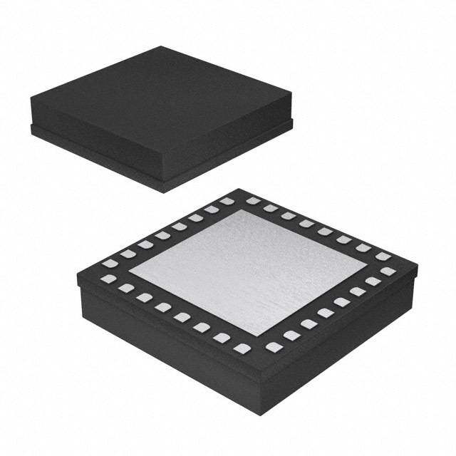
| 产品图片 |
|
| rohs | 符合RoHS无铅 / 符合限制有害物质指令(RoHS)规范要求 |
| 产品系列 | RF集成电路,调节器/解调器,Analog Devices AD8346ARUZ- |
| 数据手册 | |
| P1dB | -3dBm |
| 产品型号 | AD8346ARUZ |
| RF频率 | 800MHz ~ 2.5GHz |
| 产品目录页面 | |
| 产品种类 | 调节器/解调器 |
| 功能 | 调制器 |
| 包装 | 管件 |
| 商标 | Analog Devices |
| 安装风格 | SMD/SMT |
| 封装 | Tube |
| 封装/外壳 | 16-TSSOP(0.173",4.40mm 宽) |
| 封装/箱体 | TSSOP-16 |
| 工作温度范围 | - 40 C to + 85 C |
| 工作电压 | 2.7 V to 5.5 V |
| 工作电流 | 45 mA |
| 工作电源电压 | 2.7 V to 5.5 V |
| 工厂包装数量 | 96 |
| 接口类型 | LO |
| 最大功率耗散 | 500 mW |
| 最大工作温度 | + 85 C |
| 最小工作温度 | - 40 C |
| 本底噪声 | -147dBm/Hz |
| 标准包装 | 96 |
| 测试频率 | 1.9GHz |
| 电压-电源 | 2.7 V ~ 5.5 V |
| 电流-电源 | 55mA |
| 电源电流 | 45 mA |
| 类型 | Modulator |
| 系列 | AD8346 |
| 视频文件 | http://www.digikey.cn/classic/video.aspx?PlayerID=1364138032001&width=640&height=505&videoID=2245193150001 |
| 调制类型 | Quadrature |
| 输出功率 | -6dBm |


- 商务部:美国ITC正式对集成电路等产品启动337调查
- 曝三星4nm工艺存在良率问题 高通将骁龙8 Gen1或转产台积电
- 太阳诱电将投资9.5亿元在常州建新厂生产MLCC 预计2023年完工
- 英特尔发布欧洲新工厂建设计划 深化IDM 2.0 战略
- 台积电先进制程称霸业界 有大客户加持明年业绩稳了
- 达到5530亿美元!SIA预计今年全球半导体销售额将创下新高
- 英特尔拟将自动驾驶子公司Mobileye上市 估值或超500亿美元
- 三星加码芯片和SET,合并消费电子和移动部门,撤换高东真等 CEO
- 三星电子宣布重大人事变动 还合并消费电子和移动部门
- 海关总署:前11个月进口集成电路产品价值2.52万亿元 增长14.8%


PDF Datasheet 数据手册内容提取
0.8 GHz to 2.5 GHz Quadrature Modulator AD8346 FEATURES FUNCTIONAL BLOCK DIAGRAM High accuracy 1 degree rms quadrature error @ 1.9 GHz IBBP 1 16 QBBP 0.2 dB I/Q amplitude balance @ 1.9 GHz IBBN 2 15 QBBN Broad frequency range: 0.8 GHz to 2.5 GHz Sideband suppression: −46 dBc @ 0.8 GHz COM1 3 14 COM4 Sideband suppression: −36 dBc @ 1.9 GHz COM1 4 13 COM4 Modulation bandwidth: dc to 70 MHz LOIN 5 12 VPS2 0 dBm output compression level @ 0.8 GHz PHASE Noise floor: −147 dBm/Hz LOIP 6 SPLITTER 11 VOUT Single 2.7 V to 5.5 V supply VPS1 7 10 COM3 Quiescent operating current: 45 mA AD8346 S1t6a-lnedabdy T cSuSrOrePn t: 1 μA ENBL 8 BIAS 9 COM2 05335-001 Figure 1. APPLICATIONS Digital and spread spectrum communication systems Cellular/PCS/ISM transceivers Wireless LAN/wireless local loop QPSK/GMSK/QAM modulators Single-sideband (SSB) modulators Frequency synthesizers Image reject mixer GENERAL DESCRIPTION The AD8346 is a silicon RFIC I/Q modulator for use from This quadrature modulator can be used as the transmit mod- 0.8 GHz to 2.5 GHz. Its excellent phase accuracy and amplitude ulator in digital systems such as PCS, DCS, GSM, CDMA, and balance allow high performance direct modulation to RF. ISM transceivers. The baseband quadrature inputs are directly modulated by the LO signal to produce various QPSK and The differential LO input is applied to a polyphase network QAM formats at the RF output. phase splitter that provides accurate phase quadrature from 0.8 GHz to 2.5 GHz. Buffer amplifiers are inserted between Additionally, this quadrature modulator can be used with direct two sections of the phase splitter to improve the signal-to- digital synthesizers in hybrid phase-locked loops to generate noise ratio. The I and Q outputs of the phase splitter drive the signals over a wide frequency range with millihertz resolution. LO inputs of two Gilbert-cell mixers. Two differential V-to-I The AD8346 comes in a 16-lead TSSOP package, measuring converters connected to the baseband inputs provide the 6.5 mm × 5.1 mm × 1.1 mm. It is specified to operate over a baseband modulation signals for the mixers. The outputs of −40°C to +85°C temperature range and a 2.7 V to 5.5 V supply the two mixers are summed together at an amplifier which is voltage range. The device is fabricated on Analog Devices’ high designed to drive a 50 Ω load. performance 25 GHz bipolar silicon process. Rev. A Information furnished by Analog Devices is believed to be accurate and reliable. However, no responsibility is assumed by Analog Devices for its use, nor for any infringements of patents or other rights of third parties that may result from its use. One Technology Way, P.O. Box 9106, Norwood, MA 02062-9106, U.S.A. Specifications subject to change without notice. No license is granted by implication or otherwise under any patent or patent rights of Analog Devices. Trademarks and Tel: 781.329.4700 www.analog.com registered trademarks are the property of their respective companies. Fax: 781.461.3113 © 2005 Analog Devices, Inc. All rights reserved.
AD8346 TABLE OF CONTENTS Specifications.....................................................................................3 Bias...............................................................................................10 Absolute Maximum Ratings............................................................4 Basic Connections......................................................................11 ESD Caution..................................................................................4 LO Drive......................................................................................11 Pin Configuration and Function Descriptions.............................5 RF Output....................................................................................11 Equivalent Circuits...........................................................................6 Interface to AD9761 TXDAC®..................................................12 Typical Performance Characteristics.............................................7 AC-Coupled Interface...............................................................13 Circuit Description.........................................................................10 Evaluation Board............................................................................14 Overview......................................................................................10 Characterization Setups.................................................................16 LO Interface.................................................................................10 SSB Setup.....................................................................................16 V-to-I Converter.........................................................................10 CDMA Setup...............................................................................17 Mixers..........................................................................................10 Outline Dimensions.......................................................................18 Differential-to-Single-Ended Converter.................................10 Ordering Guide..........................................................................18 REVISION HISTORY 6/05—Rev. 0 to Rev. A Updated Format..................................................................Universal Changes to Figures 30, 31, 32........................................................14 Update Outline Dimensions.........................................................18 Changes to Ordering Guide..........................................................18 3/99—Revision 0: Initial Version Rev. A | Page 2 of 20
AD8346 SPECIFICATIONS V = 5 V; T = 25°C; LO frequency = 1900 MHz; LO level = –10 dBm; BB frequency = 100 kHz; BB inputs are dc-biased to 1.2 V; BB input S A level = 1.0 V p-p each pin for 2.0 V p-p differential drive; LO source and RF output load impedances are 50 Ω, dBm units are referenced to 50 Ω unless otherwise noted. Table 1. Parameters Conditions Min Typ Max Unit RF OUTPUT Operating Frequency 0.8 2.5 GHz Quadrature Phase Error See Figure 35 for setup 1 Degree rms I/Q Amplitude Balance See Figure 35 for setup 0.2 dB Output Power I and Q channels in quadrature −13 −10 −6 dBm Output VSWR 1.25:1 Output P1 dB −3 dBm Carrier Feedthrough −42 −35 dBm Sideband Suppression −36 −25 dBc IM3 Suppression −60 dBc Equivalent Output IP3 20 dBm Output Noise Floor 20 MHz offset from LO −147 dBm/Hz RESPONSE TO CDMA IS95 BASEBAND SIGNALS ACPR (Adjacent Channel Power Ratio) See Figure 35 for setup −72 dBc EVM (Error Vector Magnitude) See Figure 35 for setup 2.5 % Rho (Waveform Quality Factor) See Figure 35 for setup 0.9974 MODULATION INPUT Input Resistance 12 kΩ Modulation Bandwidth −3 dB 70 MHz LO INPUT LO Drive Level −12 −6 dBm Input VSWR 1.9:1 ENABLE ENBL HI Threshold 2.0 V ENBL LO Threshold 0.5 V ENBL Turn-On Time Settle to within 0.5 dB of final SSB 2.5 μs output power ENBL Turn-Off Time Time for supply current to drop below 12 μs 2 mA POWER SUPPLIES Voltage 2.7 5.5 V Current Active (ENBL HI) 35 45 55 mA Current Standby (ENBL LO) 1 20 μA Rev. A | Page 3 of 20
AD8346 ABSOLUTE MAXIMUM RATINGS Table 2. Stresses above those listed under Absolute Maximum Ratings Parameter Min Rating may cause permanent damage to the device. This is a stress Supply Voltage VPS1, VPS2 5.5 V rating only; functional operation of the device at these or any Input Power LOIP, LOIN (relative to 50 Ω) 10 dBm other condition s above those indicated in the operational Min Input Voltage IBBP, IBBN, QBBP, QBBN 0 V section of this specification is not implied. Exposure to absolute Max Input Voltage IBBP, IBBN, QBBP, QBBN 2.5 V maximum rating conditions for extended periods may affect Internal Power Dissipation 500 mW device reliability. θJA 125°C/W Operating Temperature Range −40°C to +85°C Storage Temperature Range −65°C to +150°C Lead Temperature (Soldering 60 sec) 300°C ESD CAUTION ESD (electrostatic discharge) sensitive device. Electrostatic charges as high as 4000 V readily accumulate on the human body and test equipment and can discharge without detection. Although this product features proprietary ESD protection circuitry, permanent damage may occur on devices subjected to high energy electrostatic discharges. Therefore, proper ESD precautions are recommended to avoid performance degradation or loss of functionality. Rev. A | Page 4 of 20
AD8346 PIN CONFIGURATION AND FUNCTION DESCRIPTIONS IBBP 1 16 QBBP IBBN 2 15 QBBN COM1 3 14 COM4 COM1 4 AD8346 13 COM4 TOPVIEW LOIN 5 (NottoScale) 12 VPS2 LOIP 6 11 VOUT VPS1 7 10 COM3 ENBL 8 9 COM2 05335-002 Figure 2. Pin Configuration Table 3. Pin Function Descriptions Equivalent Pin No. Mnemonic Description Circuit 1 IBBP I Channel Baseband Positive Input Pin. Input should be dc-biased to approximately 1.2 V. Circuit A Nominal characterized ac swing is 1 V p-p (0.7 V to 1.7 V). This makes the differential input 2 V p-p when IBBN is 180 degrees out of phase from IBBP. 2 IBBN I Channel Baseband Negative Input Pin. Input should be dc-biased to approximately 1.2 V. Circuit A Nominal characterized ac swing is 1 V p-p (0.7 V to 1.7 V). This makes the differential input 2 V p-p when IBBN is 180 degrees out of phase from IBBP. 3 COM1 Ground Pin for the LO phase splitter and LO buffers. 4 COM1 Ground Pin for the LO phase splitter and LO buffers. 5 LOIN LO Negative Input Pin. Internal dc bias (approximately VPS1 to 800 mV) is supplied. This Circuit B pin must be ac coupled. 6 LOIP LO Positive Input Pin. Internal dc bias (approximately VPS1 to 800 mV) is supplied. This pin Circuit B must be ac-coupled. 7 VPS1 Power Supply Pin for the bias cell and LO buffers. This pin should be decoupled using local 100 pF and 0.01 μF capacitors. 8 ENBL Enable Pin. A high level enables the device; a low level puts the device in sleep mode. Circuit C 9 COM2 Ground Pin for the input stage of output amplifier. 10 COM3 Ground Pin for the output stage of output amplifier. 11 VOUT 50 Ω DC-Coupled RF Output. User must provide ac coupling on this pin. Circuit D 12 VPS2 Power Supply Pin for baseband input voltage to current converters and mixer core. This pin should be decoupled using local 100 pF and 0.01 μF capacitors. 13 COM4 Ground Pin for baseband input voltage to current converters and mixer core. 14 COM4 Ground Pin for baseband input voltage to current converters and mixer core. 15 QBBN Q Channel Baseband Negative Input. Input should be dc biased to approximately 1.2 V. Circuit A Nominal characterized ac swing is 1 V p-p. This makes the differential input 2 V p-p when QBBN is 180° out of phase from QBBP. 16 QBBP Q Channel Baseband Positive Input. Input should be dc-biased to approximately 1.2 V. Circuit A Nominal characterized ac swing is 1 V p-p. This makes the differential input 2 V p-p when QBBN is 180° out of phase from QBBP. Rev. A | Page 5 of 20
AD8346 EQUIVALENT CIRCUITS VPS2 VPS1 BUFFER TO MIXER CORE 75kΩ 9kΩ 75kΩ TSOTA BRIATUSP F/OR INPUT 30kΩ SHUTDOWN ENBL 3kΩ ACTIVE LOADS 05335-003 40kΩ 780Ω 05335-005 Figure 3. Circuit A Figure 5. Circuit C VPS1 VPS2 LOIN PHASE SPLITTER 43Ω CONTINUES VOUT LOIP 05335-004 43Ω 05335-006 Figure 4. Circuit B Figure 6. Circuit D Rev. A | Page 6 of 20
AD8346 TYPICAL PERFORMANCE CHARACTERISTICS –6 2 T = 25°C –7 1 VP = 5.5V 0 –8 B) m) –9 VP = 5V ON (d –1 ER (dB–10 VP = 3V ARIATI ––23 W V O–11 R B P VP = 2.7V WE –4 S–12 O S P –5 T –13 PU –6 T U ––1145 05335-007 O ––780.1 1 10 10005335-010 800 1000 1200 1400 1600 1800 2000 2200 2400 LO FREQUENCY (MHz) BASEBAND FREQUENCY (MHz) Figure 7. Single Sideband (SSB) Output Power (POUT) vs. LO Frequency (FLO). Figure 10. I and Q Input Bandwidth. FLO =1900 MHz, I or Q inputs I and Q inputs driven in quadrature at baseband frequency driven with differential amplitude of 2.00 V p-p. (FBB) = 100 kHz with differential amplitude of 2.00 V p-p. –6 2 LO = 800MHz,–6dBm VP = 5V T = +85°C –7 0 VP = 5V SSB OUTPUT POWER (dBm)––––110189 LO = 1900LMOHL =zO, 1–=91 08000dM0BMHmHz,z–,6–d10BdmBm SSB OUTPUT P1dB (dBm)–1––––02468 VT P= =– 420.7°VC VT P= =+ 825.7°VCT =–40°C ––1123–40 –30 –20 –10 0 10 20 30 40 50 60 70 80 05335-008 ––1124800 1000 1200 1400 1600 1800 2000 2200 2400 05335-011 TEMPERATURE (°C) LO FREQUENCY (MHz) Figure 8. SSB POUT vs. Temperature. I and Q inputs driven in quadrature Figure 11. SSB Output 1 dB Compression Point (OP 1 dB) vs. FLO. with differential amplitude of 2.00 V p-p at FBB = 100 kHz. I and Q inputs driven in quadrature at FBB = 100 kHz. –35 30 T = +85°C T =–40°C –37 25 VP = 5.5V m)–39 dB 20 ROUGH (––4413 VP = 5V ENTAGE15 H C EDT–45 VP = 3V PER E 10 F R RIE–47 VP = 2.7V R 5 A C––4591–40 –30 –20 –10 0 10 20 30 40 50 60 70 80 05335-009 0–90 –86 –82 –78 –74 –70 –66 –62 –58 –54 –50 –4605335-012 TEMPERATURE (°C) CARRIER FEEDTHROUGH (dBm/ AFTER NULLING TO <–60dBm @ 25°C) Figure 9. Carrier Feedthrough vs. Temperature. Figure 12. Histogram Showing Carrier Feedthrough Distributions FLO = 1900 MHz, LO input level = –10 dBm. at the Temperature Extremes after Nulling at Ambient at FLO = 1900 MHz, LO Input Level = –10 dBm. Rev. A | Page 7 of 20
AD8346 –7 –30 –8 –32 VP = 5.5V –9 R (dBm)–10 VP = 3V ON (dBc) ––3346 VP = 3V VP = 5.5V OWE–11 VP = 5V ESSI UTPUT P–12 VP = 2.7V B SUPPR ––3480 VP = 5V VP = 2.7V B O–13 S S S –42 ––1145 05335-013 –44 05335-016 –40 –30 –20 –10 0 10 20 30 40 50 60 70 80 0 2 4 6 8 10 12 14 16 18 20 TEMPERATURE (°C) BASEBAND FREQUENCY (MHz) Figure 13. SSB POUT vs. Temperature. FLO = 1900 MHz, I and Q inputs driven in Figure 16. Sideband Suppression vs. FBB. FLO = 1900 MHz, I and Q inputs quadrature with differential amplitude of 2.00 V p-p at FBB = 100 kHz. driven in quadrature with differential amplitude of 2.00 V p-p. –35 –36 T = 25°C –38 VP = 5.5V –40 m) B–40 GH (d–42 VP = 3V ONICc)–45 VP = 5V U MB EEDTHRO––4446 VP = 5V HIRD HARORTION (d––5505 VP = 2.7V VP = 3V ER F–48 VP = 2.7V UT TDIST ARRI–50 INP –60 C ––5524 05335-014 ––6750 VP = 5.5V 05335-017 800 1000 1200 1400 1600 1800 2000 2200 2400 –40 –30 –20 –10 0 10 20 30 40 50 60 70 80 LO FREQUENCY (MHz) TEMPERATURE (°C) Figure 14. Carrier Feedthrough vs. FLO. Figure 17. Third Harmonic Distortion vs. Temperature. LO input level = –10 dBm. FLO =1900 MHz, I and Q inputs driven in quadrature with differential amplitude of 2.00 V p-p at FBB = 100 kHz. –32 0 T = 25°C VP = 5.5V –2 –34 c) –4 dB–36 ON ( VP = 5V B) –6 T = +25°C T =–40°C SSI–38 S (d –8 E S R O D SUPP––4402 VP = 3V TURN L––1102 T = +85°C N E BA R–14 E–44 D SI VP = 2.7V –16 ––4468 05335-015 ––2108 05335-018 900 1100 1300 1500 1700 1900 2100 2300 2500 800 1000 1200 1400 1600 1800 2000 2200 2400 LO FREQUENCY (MHz) FREQUENCY (MHz) Figure 15. Sideband Suppression vs. FLO. VPOS = 2.7 V, I and Q inputs driven in Figure 18. Return Loss of LOIN Input vs. FLO. quadrature with differential amplitude of 2.00 V p-p at FBB = 100 kHz. VPOS = 5.0 V, LOIP pin ac-coupled to ground. Rev. A | Page 8 of 20
AD8346 –30 –40 VP = 2.7V –32 –34 VP = 3V NIC –45 VP = 3V Bc) MOB)c PPRESSION (d––3368 VP = 5.5V VP = 5V VP = 2.7V UT THIRD HARDISTORTION (d––5505 VP = 5V VP = 5.5V SU–40 NP B I S –60 –42 –44 05335-019 –65 05335-022 –40 –30 –20 –10 0 10 20 30 40 50 60 70 80 0 2 4 6 8 10 12 14 16 18 20 TEMPERATURE (°C) BASEBAND FREQUENCY (MHz) Figure 19. Sideband Suppression vs. Temperature. Figure 22. Third Harmonic Distortion vs. FBB. FLO = 1900 MHz, I and Q inputs driven in quadrature FLO =1900 MHz, I and Q inputs driven in quadrature with differential amplitude of 2.00 V p-p at FBB = 100 kHz. with differential amplitude of 2.00 V p-p. –30 –6 52 –35 SSB POUT –8 50 –40 NIC –45 ––1102dBm) T (mA) 4486 VP = 5.5V MOBc)–50 R ( EN VP = 5V INPUT THIRD HARDISTORTION (d––––56675050 3RD HARMONIC –––111468SSB OUTPUT POWE SUPPLY CURR 444420 VP = 2.7VVP = 3V ––78500.5 1.0BASEBAN1D.5 DIFFEREN2T.I0AL INPUT2.5 3.0––2202 05335-020 3386–40 –20 0TEMPER2A0TURE (°4C0) 60 80 05335-023 VOLTAGE (Vp-p) Figure 20. Third Harmonic Distortion and SSB Output Figure 23. Power Supply Current vs. Temperature Power vs. Baseband Differential Input Voltage Level. FLO = 1900 MHz, I and Q inputs driven in quadrature at FBB = 100 kHz. 0 0 –5 –5 –10 –10 B) T =–40°C B) S (d–15 S (d–15 T =–40°C S S LO–20 LO–20 N N R R TU–25 TU–25 E E R T = +25°C R T = +25°C –30 –30 T = +85°C ––4305 T = +85°C 05335-021 ––4305 05335-024 800 1000 1200 1400 1600 1800 2000 2200 2400 800 1000 1200 1400 1600 1800 2000 2200 2400 FREQUENCY (MHz) FREQUENCY (MHz) Figure 21. Return Loss of VOUT Output vs. FLO. Figure 24. Return Loss of VOUT Output vs. FLO. VPOS = 2.7 V. VPOS = 5.0 V. Rev. A | Page 9 of 20
AD8346 CIRCUIT DESCRIPTION OVERVIEW V-TO-I CONVERTER The AD8346 can be divided into the following sections: local Each baseband input pin is connected to an op amp driving an oscillator (LO) interface, mixer, voltage-to-current (V-to-I) emitter follower. Feedback at the emitter maintains a current converter, differential-to-single-ended (D-to-S) converter, and proportional to the input voltage through the transistor. This bias. A detailed block diagram of the part is shown in Figure 25. current is fed to the two mixers in differential form. The LO interface generates two LO signals, with 90° of phase MIXERS difference between them, to drive two mixers in quadrature. There are two double-balanced mixers, one for the in-phase Baseband voltage signals are converted into current form in channel (I-channel) and one for the quadrature channel the V-to-I converters, feeding into two mixers. The output of (Q channel). Each mixer uses the gilbert cell design with four the mixers are combined to feed the D-to-S converter which cross-connected transistors. The bases of the transistors are provides the 50 Ω output interface. Bias currents to each driven by the LO signal of the corresponding channel. The section are controlled by the Enable (ENBL) signal. Detailed output currents from the two mixers are summed together in descriptions of each section follows. two resistors in series with two coupled on-chip inductors. The signal developed across the R-L loads is sent to the D-to-S stage. LO INTERFACE The differential LO inputs allow the user to drive the LO differ- DIFFERENTIAL-TO-SINGLE-ENDED CONVERTER entially in order to achieve maximum performance. The LO can The differential-to-single-ended converter consists of two be driven single-endedly but the LO feedthrough performance emitter followers driving a totem-pole output stage. Output is degraded, especially towards the higher end of the frequency impedance is established by the emitter resistors in the output range. The LO interface consists of interleaved stages of transistors. The output of this stage is connected to the output polyphase network phase splitters and buffer amplifiers. The (VOUT) pin. phase-splitter contains resistors and capacitors connected in a circular manner to split the LO signal into I and Q paths in BIAS precise quadrature with each other. The signal on each path A band gap reference circuit based on the Δ-V principle BE goes through a buffer amplifier to make up for the loss and high generates the proportional-to-absolute-temperature (PTAT) frequency roll-off. The two signals then go through another currents used by the different sections as references. The band polyphase network to enhance the quadrature accuracy. The gap voltage is also used to generate a temperature-stable current broad operating frequency range of 0.8 GHz to 2.5 GHz is in the V-to-I converters to produce a temperature-independent achieved by staggering the RC time constants in each stage of slew rate. When the band gap reference is disabled by pulling the phase-splitters. The outputs of the second phase-splitter are down the ENBL pin, all other sections are shut off accordingly. fed into the driver amplifiers for the mixers’ LO inputs. IBBP IBBN V-TO-I V-TO-I AD8346 MIXER LOIN PHASE PHASE SPLITTER SPLITTER D-TO-S VOUT 1 2 LOIP MIXER ENBL BIAS CELL V-TO-I V-TO-I 05335-025 QBBP QBBN Figure 25. Detailed Block Diagram Rev. A | Page 10 of 20
AD8346 BASIC CONNECTIONS The basic connections for operating the AD8346 are shown in have a bias level about 800 mV below supply. An LO drive Figure 27. A single power supply of between 2.7 V and 5.5 V is level of between −6 dBm and −12 dBm is required. For optimal applied to pins VPS1 and VPS2. A pair of ESD protection performance, a drive level of −10 dBm is recommended, diodes are connected internally between VPS1 and VPS2 so although a level of −6 dBm results in more stable temperature these must be tied to the same potential. Both pins should be performance (see Figure 8). Higher levels degrade linearity individually decoupled using 100 pF and 0.01 μF capacitors, while lower levels tend to increase the noise floor. located as close as possible to the device. For normal operation, 100pF the enable pin, ENBL, must be pulled high. The turn-on LO LOIP threshold for ENBL is 2 V. To put the device in its power-down mode, ENBL must be pulled below 0.5 V. Pins COM1 to COM4 AD8346 should all be tied to a low impedance ground plane. The I and Q ports should be driven differentially. This is con- 100pF LOIN 05335-026 venient as most modern high speed DACs have differential Figure 26. Single-Ended LO Drive outputs. For optimal performance, the drive signal should be a 2 V p-p (differential) signal with a bias level of 1.2 V, that is, The LO terminal can be driven single-ended, as shown in each input swings from 0.7 V to 1.7 V. The I and Q inputs have Figure 26 at the expense of slightly higher LO feedthrough. input impedances of 12 kΩ. By dc coupling the DAC to the LOIN is ac coupled to ground using a capacitor and LOIP is AD8346 and applying small offset voltages, the LO feedthrough driven through a coupling capacitor from a (single-ended) can be reduced to well below its nominal value of −42 dBm 50 Ω source (this scheme could also be reversed with LOIP (see Figure 12). being ac-coupled to ground). LO DRIVE RF OUTPUT The return loss of the LO port is shown in Figure 18. No add- The RF output is designed to drive a 50 Ω load, but must be ac- itional matching circuitry is required to drive this port from a coupled, as shown in Figure 27. If the I and Q inputs are driven 50 Ω source. For maximum LO suppression at the output, a in quadrature by 2 V p-p signals, the resulting output power is differential LO drive is recommended. In Figure 27, this is about −10 dBm (see Figure 7 for variations in output power achieved using a balun (M/A-COM Part Number ETC1-1-13). over frequency). The output of the balun is ac-coupled to the LO inputs which IP 1 IBBP QBBP 16 QP 2 IBBN QBBN 15 IN AD8346 QN 3 COM1 COM4 14 C6 LO 5 1 100pF 4 COM1 COM4 13 C1 C2 +VS T1 C7 5 LOIN VPS2 12 100pF 0.01μF ETC1-1-13 2 100pF 6 LOIP VOUT 11 VOUT 4 3 C5 7 VPS1 COM3 10 100pF +VS 0.01μCF4 C1030pF 8 ENBL COM2 9 05335-027 Figure 27. Basic Connections Rev. A | Page 11 of 20
AD8346 INTERFACE TO AD9761 TXDAC® Figure 28 shows a dc-coupled current output DAC interface. 10 mA, giving a voltage swing of 0 V to 1 V (at the DAC The use of dual-integrated DACs, such as the AD9761 with output). This results in a 0.5 V p-p swing at the I and Q inputs specified ±0.02 dB and ±0.004 dB gain and offset matching of the AD8346 (resulting in a 1 V p-p differential swing). characteristics, ensures minimum error contribution (over Note that the ratio matching characteristics of the resistive temperature) from this portion of the signal chain. The use of a network, as opposed to its absolute accuracy, is critical in precision thin-film resistor network sets the bias levels precisely preserving the gain and offset balance between the I and Q to prevent the introduction of offset errors, which increase LO signal path. feedthrough. For instance, selecting resistor networks with a 0.1% ratio matching characteristics maintains 0.03 dB gain and By applying small dc offsets to the I and Q signals from the offset matching performance. DAC, the LO suppression can be reduced from its nominal value of −42 dBm to as low as −60 dBm while holding to Using resistive division, the dc bias level at the I and Q inputs approximately −50 dBm over temperature (see Figure 12 for to the AD8346 is set to approximately 1.2 V. Each of the four a plot of LO feedthrough over temperature for an offset current outputs of the DAC delivers a full-scale current of compensated circuit). 5V +5V 634Ω 0.1μF DVDD DCOM AVDD 500Ω 500Ω VPS1 VPS2 100Ω IOUTA 500Ω IBBP LATICH 2× DAIC IOUTB CFILTER VOUT 100Ω 500Ω IBBN Σ DAC DATA INPUTS AD9761 500Ω 500Ω LOIP 100Ω PHASE QOUTA 500Ω QBBP SPLITTER LAQTCH 2× DAQC QOUTB CFILTER LOIN 500Ω QBBN SELECT 100Ω MUX 0.5V p-p EACH PIN AD8346 WRITE CONTROL WITH VCM = 1.2V CLOCK SLEEP FS ADJ REFIO R2SkEΩT 0.1μF 05335-028 Figure 28. AD8346 Interface to AD9761 TxDAC Rev. A | Page 12 of 20
AD8346 AC-COUPLED INTERFACE An ac-coupled interface can also be implemented, as shown in The network shown has a high-pass corner frequency of Figure 29. This is an advantage because there is almost no approximately 14.3 kHz (note that the 12 kΩ input impedance voltage loss due to the biasing network, allowing the AD8346 of the AD8346 has been factored into this calculation). inputs to be driven by the full 2 V p-p differential signal from Increasing the resistors in the network or increasing the the AD9761 (each of the DAC’s 4 outputs delivering 1 V p-p). coupling capacitance reduces the corner frequency further. As in the dc-coupled case, the bias levels on the I and Q inputs Note that the LO suppression can be manually optimized by should be set to as precise a level as possible, relative to each replacing a portion of the four top 2.43 kΩ resistors with other. This prevents the introduction of additional input offset potentiometers. In this case, the bottom four resistors in the voltages. In Figure 29, the bias level on each input is set to biasing network no longer need to be precision devices. approximately 1.2 V. The 2.43 kΩ resistors should have a ratio tolerance of 0.1% or better. 5V 5V 1kΩ 0.1μF DVDD DCOM AVDD 2.43kΩ 2.43kΩ IOUTA 100Ω 0.01μF IBBP VPS1 VPS2 LATICH 2× DAIC IOUTB CFILTER 2.43kΩ VOUT 100Ω 0.01μF 2.43kΩ IBBN Σ DAC DATA AD9761 INPUTS LOIP 100Ω 0.01μF 2.43kΩ 2.43kΩ PHASE QOUTA QBBP SPLITTER LAQTCH 2× DQAC QOUTB CFILTER 2.43kΩ LOIN QBBN SELECT 100Ω 0.01μF AD8346 MUX 2.43kΩ WRITE CONTROL 1V p-p EACH PIN CLOCK SLEEP FS ADJ REFIO WITH VCM = 1.2V R2SkEΩT 0.1μF 05335-029 Figure 29. AC-Coupled DAC Interface Rev. A | Page 13 of 20
AD8346 EVALUATION BOARD The schematic of the AD8346 evaluation board is shown in All connectors are of the SMA type. The I and Q inputs are Figure 30. This is a 4-layer FR4 board; the two center layers are provided with pads for implementing a simple RC filter used as ground planes and the top and bottom layers are used network. The local oscillator input is driven through a balun for signal and power. Figure 31 shows the layout and Figure 32 (M/A-COM Part Number ETC1-1-13). shows the silkscreen. The evaluation board circuit closely follows the basic connections circuit shown in Figure 27. Slide SW1 to the A position to connect the ENBL pin to +V S via the 10 kΩ pull-up resistor REP. Slide SW1 to the B position to disable the device by grounding the ENOP pin through the 49.9 Ω pull-down resistor REG. The device may be enabled via an external voltage applied to the SMA connector ENOP or TP2. CIP CQP RIP OPEN AD8346 OPEN RQP IP 1 IBBP QBBP 16 QP 0Ω RIS RQS 0Ω RIN OPEN OPEN RQN IN 2 IBBN QBBN 15 QN 0Ω CIN CQN 0Ω OPEN OPEN 3 COM1 COM4 14 4 COM1 COM4 13 RLON CLON OPEN 100pF R2 LO RLOS 5 T1 1 CLOP 5 LOIN VPS2 12 C4 0Ω C3 +VS OPEN ETC1-1-13 2 100pF 100pF 0.01μF 6 LOIP VOUT 11 4 3 RLOP CVO OPEN 7 VPS1 COM3 10 100pF TP2 VOUT ENOP +VS 8 ENBL COM2 9 C1 R7 C2 0.01μF 0Ω 100pF REP 10kΩ A ENOP SW1 B R49E.G9kΩ 05335-030 Figure 30. Evaluation Board Schematic Rev. A | Page 14 of 20
AD8346 05335-031 Figure 31. Layout of Evaluation Board 05335-032 Figure 32. Silkscreen of Evaluation Board Rev. A | Page 15 of 20
AD8346 CHARACTERIZATION SETUPS SSB SETUP Two main setups were used to characterize this product. These the AD8346 evaluation board can be found in Figure 30). setups are shown in Figure 33 and Figure 35. Figure 33 shows The two HP34907 plug-ins were used to provide additional the setup used to evaluate the product as an SSB. The AD8346 miscellaneous dc and control signals to the motherboard. The motherboard had circuitry that converted the single-ended LO was driven by an RF signal generator (through the balun on I and Q inputs from the arbitrary function generator to differ- the evaluation board to present a differential LO signal to the ential inputs with a dc bias of approximately 1.2 V. In addition, device) and the output was measured with a spectrum analyzer. the motherboard also provided connections for power supply With the I channel driven with a sine wave and the Q channel routing. The HP34970A and its associated plug-in 34901 were driven with a cosine wave, the lower sideband is the single used to monitor power supply currents and voltages being sideband output. The typical SSB output spectrum is shown in supplied to the AD8346 evaluation board (a full schematic of Figure 34. IEEE HP34970A D1 D2 D3 34901 34907 34907 D1 D2 D3 TEKAFG2020 +15V MAX VPS1 IIN OUTPUT1 COM AD8346 QIN OUTPUT2 IEEE IEEE +–2255VV MMAAXX VN MOTHERBOARD ARB FUNC. GEN GND HP3631 VP P1 IN IP QP QN IP QP HP8593E IN AD8346 QN HP8648C EVAL BOARD SWEEP OUT IEEE RFOUT LO VOUT RF I/P 28VOLT ENBL P1 CAL OUT IEEE IEEE SAPNEACLTYRZUEMR 05335-033 PC CONTROLLER Figure 33. Evaluation Board SSB Test Setup 0 –10 –20 –30 –40 –50 –60 –70 –80 ––10900 05335-034 CENTER 1.9GHz 50kHz/ SPAN 500kHz Figure 34. Typical SSB Output Spectrum Rev. A | Page 16 of 20
AD8346 CDMA SETUP For evaluating the AD8346 with CDMA waveforms, the setup For measuring ACPR, the I/Q input signals used were generated shown in Figure 35 was used. This is essentially the same setup with Pilot (Walsh Code 00), Sync (WC 32), Paging (WC 01), as that used for the single sideband characterization, except that and 6 Traffic (WC 08, 09, 10, 11, 12, 13) channels active. The the AFG2020 was replaced with the AWG2021 for providing the I/Q SIM software was set for 32× oversampling and was using a I and Q input signals, and the spectrum analyzer used to monitor BS equifilter. Figure 36 shows the typical output spectrum for the output was changed to an FSEA30 Rohde & Schwarz analyzer this configuration. The ACPR was measured 885 kHz away with vector demodulation capability. The I/Q input signals for from the carrier frequency. these measurements were IS95 baseband signals generated with For performing EVM, Rho, phase, and amplitude balance Tektronix I/Q SIM software and downloaded to the AWG2021. measurements, the I/Q input signals used were generated with only the pilot channel (Walsh Code 00) active. The I/Q SIM software was set for 32× oversampling using a CDMA equifilter. IEEE HP34970A D1 D2 D3 34901 34907 34907 D1 D2 D3 TEKAFG2020 +15V MAX VPS1 IIN OUTPUT1 COM AD8346 QIN OUTPUT2 IEEE IEEE +–2255VV MMAAXX VN MOTHERBOARD ARB FUNC. GEN GND HP3631 VP P1 IN IP QP QN IP QP IN AD8346 QN HP8648C EVAL BOARD FSEA30 IEEE RFOUT LO VOUT RF I/P IEEE ENBL P1 SPECTRUM ANALYZER IEPECE CONTROLLER 05335-035 Figure 35. Evaluation Board CDMA Test Setup –20 –30 –40 –50 –60 CH PWR =–20.7dBm ACP UPR =–71.8dBc –70 ACP LWR =–71.7dBc –80 –90 –100 ––111200 05335-036 CENTER 1.9GHz 187.5kHz/ SPAN 1.875MHz Figure 36. Typical CDMA Output Spectrum Rev. A | Page 17 of 20
AD8346 OUTLINE DIMENSIONS 5.10 5.00 4.90 16 9 4.50 6.40 4.40 BSC 4.30 1 8 PIN 1 1.20 MAX 0.15 0.20 0.05 0.09 0.75 0.30 8° 0.60 0.65 0.19 SEATING 0° 0.45 BSC PLANE COPLANARITY 0.10 COMPLIANT TO JEDEC STANDARDS MO-153AB Figure 37.16-Lead Thin Shrink Small Outline Package [TSSOP] (RU-16) Dimensions shown in millimeters ORDERING GUIDE Model Temperature Range Package Description Package Option AD8346ARU −40°C to +85°C 16-Lead Thin Shrink Small Outline Package (TSSOP) RU-16 AD8346ARU-REEL −40°C to +85°C 16-Lead (TSSOP) 13" Tape and Reel RU-16 AD8346ARU-REEL7 −40°C to +85°C 16-Lead (TSSOP) 7" Tape and Reel RU-16 AD8346ARUZ-REEL1 −40°C to +85°C 16-Lead (TSSOP) 13" Tape and Reel RU-16 AD8346ARUZ-REEL71 −40°C to +85°C 16-Lead (TSSOP) 7" Tape and Reel RU-16 AD8346-EVAL Evaluation Board 1 Z = Pb-free part. Rev. A | Page 18 of 20
AD8346 NOTES Rev. A | Page 19 of 20
AD8346 NOTES ©2005 Analog Devices, Inc. All rights reserved. Trademarks and registered trademarks are the property of their respective companies. C05335–0–6/05(A) Rev. A | Page 20 of 20