ICGOO在线商城 > 射频/IF 和 RFID > RF 调制器 > ADL5386ACPZ-R7
 Datasheet下载
- 型号: ADL5386ACPZ-R7
- 制造商: Analog
- 库位|库存: xxxx|xxxx
- 要求:
| 数量阶梯 | 香港交货 | 国内含税 |
| +xxxx | $xxxx | ¥xxxx |
查看当月历史价格
查看今年历史价格
ADL5386ACPZ-R7产品简介:
ICGOO电子元器件商城为您提供ADL5386ACPZ-R7由Analog设计生产,在icgoo商城现货销售,并且可以通过原厂、代理商等渠道进行代购。 ADL5386ACPZ-R7价格参考。AnalogADL5386ACPZ-R7封装/规格:RF 调制器, RF Modulator IC 50MHz ~ 2.2GHz 40-VFQFN Exposed Pad, CSP。您可以下载ADL5386ACPZ-R7参考资料、Datasheet数据手册功能说明书,资料中有ADL5386ACPZ-R7 详细功能的应用电路图电压和使用方法及教程。
ADL5386ACPZ-R7 是 Analog Devices Inc. 生产的一款 RF 调制器,主要用于射频 (RF) 和微波通信系统。这款器件在多种应用场景中具有广泛的应用价值,特别是在需要高效、低失真调制的场合。

 应用场景

1. 无线通信系统:
   ADL5386ACPZ-R7 可用于无线基站、蜂窝网络和 Wi-Fi 设备中的 RF 发射链路。它能够将基带信号调制成 RF 信号,支持多种调制方式,如 QAM、QPSK 等。其高线性度和低噪声特性使其非常适合于要求严格的通信标准,如 LTE、5G 和 WiMAX。

2. 卫星通信:
   在卫星通信系统中,ADL5386ACPZ-R7 可以用于上变频器部分,将中频 (IF) 信号转换为射频信号,以便通过卫星链路传输。其宽带宽和高动态范围特性使得它能够在不同频率范围内工作,适应不同的卫星通信需求。

3. 测试与测量设备:
   对于 RF 测试仪器,如信号发生器和频谱分析仪,ADL5386ACPZ-R7 可以提供精确的调制功能,帮助工程师进行复杂的信号分析和测试。其优异的相位噪声性能和稳定性确保了测试结果的准确性。

4. 雷达系统:
   在雷达应用中,ADL5386ACPZ-R7 可用于发射机部分,生成高质量的调制信号。其快速响应时间和低失真特性有助于提高雷达系统的分辨率和探测精度,适用于气象雷达、军事雷达等多种类型。

5. 物联网 (IoT) 设备:
   随着 IoT 设备的普及,对高效 RF 传输的需求也在增加。ADL5386ACPZ-R7 可用于 IoT 网关和传感器节点中的 RF 发射模块,支持多种无线协议,如 Zigbee、LoRa 等,确保数据传输的可靠性和稳定性。

 总结

ADL5386ACPZ-R7 凭借其卓越的性能和灵活性,在无线通信、卫星通信、测试测量、雷达系统和物联网等领域展现出强大的应用潜力。其高集成度和易于使用的特点,使得设计人员可以更方便地将其应用于各种复杂系统中,满足多样化的需求。
| 参数 | 数值 |
| 产品目录 | |
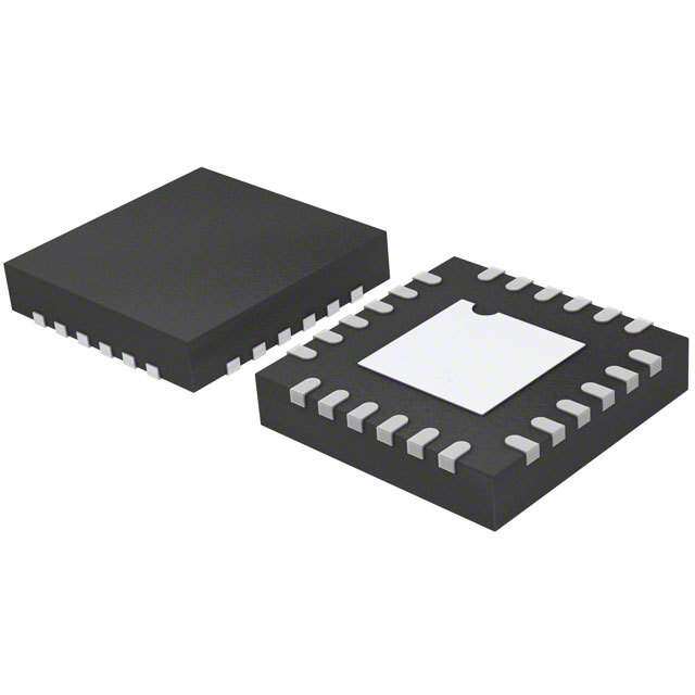
| 描述 | IC QUADRATURE MOD 50MHZ 40LFCSP |
| 产品分类 | |
| LO频率 | - |
| 品牌 | Analog Devices Inc |
| 数据手册 | |
| 产品图片 |
|
| P1dB | 8.4dBm |
| 产品型号 | ADL5386ACPZ-R7 |
| RF频率 | 50MHz ~ 2.2GHz |
| rohs | 无铅 / 符合限制有害物质指令(RoHS)规范要求 |
| 产品系列 | - |
| 其它名称 | ADL5386ACPZ-R7DKR |
| 功能 | 调制器 |
| 包装 | Digi-Reel® |
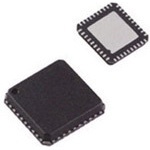
| 封装/外壳 | 40-VFQFN 裸露焊盘,CSP |
| 本底噪声 | -160dBm/Hz |
| 标准包装 | 1 |
| 测试频率 | 2.15GHz |
| 电压-电源 | 4.75 V ~ 5.5 V |
| 电流-电源 | 230mA |
| 视频文件 | http://www.digikey.cn/classic/video.aspx?PlayerID=1364138032001&width=640&height=505&videoID=2245193150001 |
| 输出功率 | 2.5dBm |


- 商务部:美国ITC正式对集成电路等产品启动337调查
- 曝三星4nm工艺存在良率问题 高通将骁龙8 Gen1或转产台积电
- 太阳诱电将投资9.5亿元在常州建新厂生产MLCC 预计2023年完工
- 英特尔发布欧洲新工厂建设计划 深化IDM 2.0 战略
- 台积电先进制程称霸业界 有大客户加持明年业绩稳了
- 达到5530亿美元!SIA预计今年全球半导体销售额将创下新高
- 英特尔拟将自动驾驶子公司Mobileye上市 估值或超500亿美元
- 三星加码芯片和SET,合并消费电子和移动部门,撤换高东真等 CEO
- 三星电子宣布重大人事变动 还合并消费电子和移动部门
- 海关总署:前11个月进口集成电路产品价值2.52万亿元 增长14.8%


PDF Datasheet 数据手册内容提取
50 MHz to 2200 MHz Quadrature Modulator with Integrated Detector and VVA ADL5386 FEATURES In addition, the ADL5386 incorporates a standalone logarithmic power detector, as well as a voltage variable Output frequency range: 50 MHz to 2200 MHz attenuator (VVA). The attenuator has its own separate input and 1 dB output compression: 11 dBm @ 350 MHz output pins for easy cascading with filters and buffer amplifiers. Noise floor: −160 dBm/Hz @ 350 MHz The wide dynamic range of the power detector and VVA provides Sideband suppression: −46 dBc @ 350 MHz flexibility in the choice of the signal monitoring point in the Carrier feedthrough: −38 dBm @ 350 MHz transmitter system. 30 dB of linear AGC dynamic range @ 350 MHz Single supply: 4.75 V to 5.5 V The wide baseband input bandwidth of 700 MHz allows for 40-lead, Pb-free LFCSP_VQ with exposed paddle either baseband drive or a drive from a complex IF signal. Typical applications are in IF or direct-to-RF radio-link transmitters, cable modem termination systems, broadband APPLICATIONS wireless access systems, and cellular infrastructure equipment. Radio-link infrastructures The ADL5386 takes signals from two differential baseband inputs Cable modem termination systems and modulates them onto two carriers in quadrature with each Wireless/cellular infrastructure systems other. The two internal carriers are derived from a single-ended, Wireless local loops external local oscillator (LO) input signal at twice the frequency WiMAX/broadband wireless access systems as the desired output. The output amplifier is designed to drive a 50 Ω load. GENERAL DESCRIPTION The ADL5386 consists of two die, one fabricated using the The ADL5386 is a quadrature modulator with unmatched Analog Devices, Inc., advanced SiGe bipolar process, and the other integration levels for low intermediate frequency (IF) and radio using an external GaAs process. The ADL5386 is packaged in a frequency (RF) transmitters within broadband wireless access 40-lead, Pb-free LFCSP_VQ with an exposed paddle. Performance systems, microwave radio links, cable modem termination is specified over the −40°C to +85°C range. A Pb-free evaluation systems, and cellular infrastructure equipment. The ADL5386 board is also available. operates over a frequency range of 50 MHz to 2200 MHz. Its excellent phase accuracy and amplitude balance supports high data rate, complex modulation for next-generation communication infrastructure equipment. FUNCTIONAL BLOCK DIAGRAM VPOS VPOS ENBL MODOUTATTI NC 38 37 36 35 23 22 21 24 10 12 9 IBBP 25 IBBN 26 IQ MOD BIAS 17ATTCM 14ATTCM LOIP 33 QUADRATURE 15dB PHASE 20ATTO LOIN 34 SPLITTER ADL5386 6 VREF QBBN 29 QBBP 30 I V 7 VDET/VCTL LOG 4 CLPF DETECTOR TEMPERATURE SENSOR I V 3 VSET TE8MP IN1LO IN2HI TA3D9J 5 11 13 15C16OM18M19 27 28 31 32 40 07664-001 Figure 1. Rev. 0 Information furnished by Analog Devices is believed to be accurate and reliable. However, no responsibility is assumed by Analog Devices for its use, nor for any infringements of patents or other One Technology Way, P.O. Box 9106, Norwood, MA 02062-9106, U.S.A. rights of third parties that may result from its use. Specifications subject to change without notice. No license is granted by implication or otherwise under any patent or patent rights of Analog Devices. Tel: 781.329.4700 www.analog.com Trademarks and registered trademarks are the property of their respective owners. Fax: 781.461.3113 ©2009 Analog Devices, Inc. All rights reserved.
ADL5386 TABLE OF CONTENTS Features .............................................................................................. 1 Open-Loop Power Control Mode ............................................ 21 Applications ....................................................................................... 1 Power Supply and Grounding .................................................. 22 General Description ......................................................................... 1 Device Enable and Disable ........................................................ 22 Functional Block Diagram .............................................................. 1 Baseband Inputs ......................................................................... 22 Revision History ............................................................................... 2 LO Input ...................................................................................... 22 Specifications ..................................................................................... 3 AGC Mode .................................................................................. 22 Typical Input and Output Impedances ...................................... 8 Setting the TADJ Resistor .......................................................... 24 Absolute Maximum Ratings ............................................................ 9 Using the Detector in Standalone Measurement Mode ........ 25 ESD Caution .................................................................................. 9 DAC Modulator Interfacing ..................................................... 25 Pin Configuration and Function Descriptions ........................... 10 Spectral Products from Harmonic Mixing ............................. 27 Typical Performance Characteristics ........................................... 12 LO Generation Using PLLs ....................................................... 27 Modulator .................................................................................... 12 Transmit DAC Options ............................................................. 28 Voltage Variable Attentuator ..................................................... 16 Modulator/Demodulator Options ........................................... 28 Detector ....................................................................................... 17 Evaluation Board ............................................................................ 29 Closed-Loop AGC Mode........................................................... 18 Characterization Setup .................................................................. 31 Circuit Description ......................................................................... 19 SSB Setup ..................................................................................... 31 Overview ...................................................................................... 19 Detector Setup ............................................................................ 31 Quadrature Modulator Section ................................................ 19 VVA S-Paramters Setup ............................................................. 32 Logarithmic Detector ................................................................. 20 VVA Intermodulation Test Setup ............................................. 32 Voltage Variable Attenuator (VVA) ......................................... 20 Outline Dimensions ....................................................................... 33 Basic Connections .......................................................................... 21 Ordering Guide .......................................................................... 33 REVISION HISTORY 1/09—Revision 0: Initial Version Rev. 0 | Page 2 of 36
ADL5386 SPECIFICATIONS Unless otherwise noted, V = 5 V, T = 25°C, LO = −7 dBm, I/Q inputs = 1.4 V p-p differential sine waves in quadrature on a 500 mV dc S A bias, baseband frequency = 1 MHz, LO source and RF output load impedances are 50 Ω. Table 1. Parameter Conditions Min Typ Max Unit MODULATOR DYNAMIC CHARACTERISTICS Operating Frequency Range 50 2200 MHz External LO Frequency Range External LO frequency is twice output frequency 100 4400 MHz Output Frequency = 50 MHz Output Power Single (lower) sideband output 5.6 dBm Modulator Voltage Gain −1.3 dB Output P1dB 10.8 dBm Output Return Loss −21 dB Carrier Leakage Unadjusted (nominal drive level) −43 dBm At 85°C after optimization at 25°C −63 dBm At −40°C after optimization at +25°C −63 dBm Sideband Suppression Unadjusted (nominal drive level) −48 dBc At 85°C after optimization at 25°C −60 dBc At −40°C after optimization at +25°C −60 dBc Quadrature Error −0.2 Degrees I/Q Amplitude Balance 0.05 dB Second Harmonic (f − (2 × f )), P = 5 dBm −80 dBc LO BB OUT Third Harmonic (f + (3 × f )), P = 5 dBm −58 dBc LO BB OUT Output IP2 F1 = 3.5 MHz, F2 = 4.5 MHz, P = −3 dBm per tone 76 dBm OUT Output IP3 F1 = 3.5 MHz, F2 = 4.5 MHz, P = −3 dBm per tone 26 dBm OUT Noise Floor 20 MHz offset from LO, all BB inputs at a bias of 500 mV −159 dBm/Hz Output Frequency = 140 MHz Output Power Single (lower) sideband output 5.7 dBm Modulator Voltage Gain −1.2 dB Output P1dB 11.1 dBm Output Return Loss −21 dB Carrier Leakage Unadjusted (nominal drive level) −42 dBm At 85°C after optimization at 25°C −62 dBm At −40°C after optimization at +25°C −62 dBm Sideband Suppression Unadjusted (nominal drive level) −57 dBc At 85°C after optimization at 25°C −60 dBc At −40°C after optimization at +25°C −60 dBc Quadrature Error −0.2 Degrees I/Q Amplitude Balance 0.05 dB Second Harmonic (f − (2 × f )), P = 5 dBm −79 dBc LO BB OUT Third Harmonic (f + (3 × f )), P = 5 dBm −56 dBc LO BB OUT Output IP2 F1 = 3.5 MHz, F2 = 4.5 MHz, P = −3 dBm per tone 75 dBm OUT Output IP3 F1 = 3.5 MHz, F2 = 4.5 MHz, P = −3 dBm per tone 25 dBm OUT Noise Floor 20 MHz offset from LO, all BB inputs at a bias of 500 mV −160 dBm/Hz Output Frequency = 350 MHz Output Power Single (lower) sideband output 4 5.5 7 dBm Modulator Voltage Gain −1.4 dB Output P1dB 11.1 dBm Output Return Loss −19 dB Carrier Leakage Unadjusted (nominal drive level) −38 dBm At 85°C after optimization at 25°C −58 dBm At −40°C after optimization at +25°C −58 dBm Rev. 0 | Page 3 of 36
ADL5386 Parameter Conditions Min Typ Max Unit Sideband Suppression Unadjusted (nominal drive level) −46 dBc At 85°C after optimization at 25°C −57 dBc At −40°C after optimization at +25°C −57 dBc Quadrature Error −0.5 Degrees I/Q Amplitude Balance 0.05 dB Second Harmonic (f − (2 × f )), P = 5 dBm −76 dBc LO BB OUT Third Harmonic (f + (3 × f )), P = 5 dBm −53 dBc LO BB OUT Output IP2 F1 = 3.5 MHz, F2 = 4.5 MHz, P = −3 dBm per tone 74 dBm OUT Output IP3 F1 = 3.5 MHz, F2 = 4.5 MHz, P = −3 dBm per tone 25 dBm OUT Noise Floor 20 MHz offset from LO, all BB inputs at a bias of 500 mV −160 dBm/Hz 20 MHz offset from LO, output power = −5 dBm −156 dBm/Hz Output Frequency = 860 MHz Output Power Single (lower) sideband output 3.8 5.3 6.8 dBm Modulator Voltage Gain −1.6 dB Output P1dB 11.4 dBm Output Return Loss −15 dB Carrier Leakage Unadjusted (nominal drive level) −37 dBm At 85°C after optimization at 25°C −56 dBm At −40°C after optimization at +25°C −56 dBm Sideband Suppression Unadjusted (nominal drive level) −39 dBc At 85°C after optimization at 25°C −55 dBc At −40°C after optimization at +25°C −55 dBc Quadrature Error −0.9 Degrees I/Q Amplitude Balance 0.05 dB Second Harmonic (f − (2 × f )), P = 5 dBm −72 dBc LO BB OUT Third Harmonic (f + (3 × f )), P = 5 dBm −49 dBc LO BB OUT Output IP2 F1 = 3.5 MHz, F2 = 4.5 MHz, P = −3 dBm per tone 73 dBm OUT Output IP3 F1 = 3.5 MHz, F2 = 4.5 MHz, P = −3 dBm per tone 25 dBm OUT Noise Floor 20 MHz offset from LO, all BB inputs at a bias of 500 mV −160 dBm/Hz 20 MHz offset from LO, output power = −5 dBm −157 dBm/Hz Output Frequency = 1450 MHz Output Power Single (lower) sideband output 4.3 dBm Modulator Voltage Gain −2.6 dB Output P1dB 10.6 dBm Output Return Loss −15 dB Carrier Leakage Unadjusted (nominal drive level) −35 dBm At 85°C after optimization at 25°C −50 dBm At −40°C after optimization at +25°C −50 dBm Sideband Suppression Unadjusted (nominal drive level) −43 dBc At 85°C after optimization at 25°C −45 dBc At −40°C after optimization at +25°C −45 dBc Quadrature Error −0.2 Degrees I/Q Amplitude Balance 0.03 dB Second Harmonic (f − (2 × f )), P = 5 dBm −67 dBc LO BB OUT Third Harmonic (f + (3 × f )), P = 5 dBm −45 dBc LO BB OUT Output IP2 F1 = 3.5 MHz, F2 = 4.5 MHz, P = −3 dBm per tone 63 dBm OUT Output IP3 F1 = 3.5 MHz, F2 = 4.5 MHz, P = −3 dBm per tone 25 dBm OUT Noise Floor 20 MHz offset from LO, all BB inputs at a bias of 500 mV −160 dBm/Hz Rev. 0 | Page 4 of 36
ADL5386 Parameter Conditions Min Typ Max Unit Output Frequency = 1900 MHz Output Power Single (lower) sideband output 3.2 dBm Modulator Voltage Gain −3.7 dB Output P1dB 9.2 dBm Output Return Loss −13 dBm Carrier Leakage Unadjusted (nominal drive level) −35 dBm At 85°C after optimization at 25°C −53 dBm At −40°C after optimization at +25°C −53 dBm Sideband Suppression Unadjusted (nominal drive level) −30 dBc At 85°C after optimization at 25°C −45 dBc At −40°C after optimization at +25°C −45 dBc Quadrature Error −3 Degrees I/Q Amplitude Balance 0.02 dB Second Harmonic (f − (2 × f )), P = 5 dBm −59 dBc LO BB OUT Third Harmonic (f + (3 × f )), P = 5 dBm −45 dBc LO BB OUT Output IP2 F1 = 3.5 MHz, F2 = 4.5 MHz, P = −3 dBm per tone 55 dBm OUT Output IP3 F1 = 3.5 MHz, F2 = 4.5 MHz, P = −3 dBm per tone 23 dBm OUT Noise Floor 20 MHz offset from LO, all BB inputs at a bias of 500 mV −160 dBm/Hz 20 MHz offset from LO, output power = −5 dBm −156 dBm/Hz Output Frequency = 2150 MHz Output Power Single (lower) sideband output 2.5 dBm Modulator Voltage Gain −4.4 dB Output P1dB 8.4 dBm Output Return Loss −11 dB Carrier Leakage Unadjusted (nominal drive level) −35 dBm At 85°C after optimization at 25°C −48 dBm At −40°C after optimization at +25°C −46 dBm Sideband Suppression Unadjusted (nominal drive level) −34 dBc At 85°C after optimization at 25°C −45 dBc At −40°C after optimization at +25°C −45 dBc Quadrature Error −1.2 Degrees I/Q Amplitude Balance 0.03 dB Second Harmonic (f − (2 × f )), P = 5 dBm −56 dBc LO BB OUT Third Harmonic (f + (3 × f )), P = 5 dBm −48 dBc LO BB OUT Output IP2 F1 = 3.5 MHz, F2 = 4.5 MHz, P = −3 dBm per tone 53 dBm OUT Output IP3 F1 = 3.5 MHz, F2 = 4.5 MHz, P = −3 dBm per tone 21 dBm OUT Noise Floor 20 MHz offset from LO, all BB inputs at a bias of 500 mV −160 dBm/Hz 20 MHz offset from LO, output power = −5 dBm −155 dBm/Hz LO Inputs Pin LOIP and Pin LOIN LO Drive Level Characterization performed at typical level −13 −7 +2 dBm Characterization performed at typical level (<140 MHz) −7 −7 +2 dBm Input Impedance 50 Ω Input Return Loss 350 MHz, LOIN ac-coupled to ground −7 dB Baseband Inputs Pin IBBP, Pin IBBN, Pin QBBP, Pin QBBN I and Q Input Bias Level 500 mV Input Bias Current −60 μA Bandwidth (0.1 dB) f = 2 × 900 MHz, P ≈ −4 dBm 50 MHz LO OUT Bandwidth (3 dB) f = 2 × 900 MHz, P ≈ −4 dBm 700 MHz LO OUT Rev. 0 | Page 5 of 36
ADL5386 Parameter Conditions Min Typ Max Unit VOLTAGE VARIABLE ATTENUATOR Pin VCTL, Pin ATTI, and Pin ATTO, open-loop mode, attenuation control applied to VCTL Output Frequency = 50 MHz Insertion Loss Minimum attenuation, V = 2 V 1.7 dB VCTL Attenuation Range Attenuation at V = 2 V − Attenuation at V = 0 V 37.8 dB VCTL VCTL Return Loss 17 dB Input IP3 Minimum attenuation, V = 2 V, Δf = 1 MHz, 36 dBm VCTL input power = −3 dBm per tone Output Frequency = 140 MHz Insertion Loss Minimum attenuation, V = 2 V 1.9 dB VCTL Attenuation Range Attenuation at V = 2 V − Attenuation at V = 0 V 37 dB VCTL VCTL Return Loss 17 dB Input IP3 Minimum attenuation, V = 2 V, Δf = 1 MHz, 36 dBm VCTL input power = −3 dBm per tone Output Frequency = 350 MHz Insertion Loss Minimum attenuation, V = 2 V 2.2 dB VCTL Attenuation Range Attenuation at V = 2 V − Attenuation at V = 0 V 26.2 dB VCTL VCTL Return Loss 17 dB Input IP3 Minimum attenuation, V = 2 V, Δf = 1 MHz, 35 dBm VCTL input power = −3 dBm per tone Output Frequency = 860 MHz Insertion Loss Minimum attenuation, V = 2 V 2.5 dB VCTL Attenuation Range Attenuation at V = 2 V − Attenuation at V = 0 V 21 dB VCTL VCTL Return Loss 14 dB Input IP3 Minimum attenuation, V = 2 V, Δf = 1 MHz, 35 dBm VCTL input power = −3 dBm per tone Output Frequency = 1900 MHz Insertion Loss Minimum attenuation, V = 2 V 3 dB VCTL Attenuation Range Attenuation at V = 2 V − Attenuation at V = 0 V 19 dB VCTL VCTL Return Loss 13 dB Input IP3 Minimum attenuation, V = 2 V, Δf = 1 MHz, 36 dBm VCTL input power = −3 dBm per tone Output Frequency = 2150 MHz Insertion Loss Minimum attenuation, V = 2 V 3.3 dB VCTL Attenuation Range Attenuation at V = 2 V − Attenuation at V = 0 V 17 dB VCTL VCTL Return Loss 13 dB Input IP3 Minimum attenuation, V = 2 V, Δf = 1 MHz, 35 dBm VCTL input power = −3 dBm per tone SWITCHING CHARACTERISTICS ATTCM (Pin 14 and Pin 17) = 1000 pF VCTL Response Time Frequency = 350 MHz, V = 2 V to 0 V; measured from 125 ns VCTL 50 % of V to10% of RF envelope VCTL Frequency = 350 MHz, V = 0 V to 2 V; measured from 15 ns VCTL 50 % of V to 90% of RF envelope VCTL LOG DETECTOR In measurement mode, VDET/VCTL is shorted to VSET; in controller mode, the setpoint voltage is applied to VSET; the CW input signal is applied at INHI f = 50 MHz R = 22.1 kΩ TADJ ±1 dB Dynamic Range T = 25°C 28 dB A Slope1 −21 mV/dB Intercept1 18.2 dBm VDET or VSET Voltage P = −10 dBm 0.59 V IN P = −30 dBm 1.01 V IN Rev. 0 | Page 6 of 36
ADL5386 Parameter Conditions Min Typ Max Unit f = 140 GHz R = 22.1 kΩ TADJ ±1 dB Dynamic Range T = 25°C 28 dB A Slope1 −21.1 mV/dB Intercept1 17.8 dBm VDET or VSET Voltage P = −10 dBm 0.59 V IN P = −30 dBm 1.01 V IN f = 350 MHz R = 22.1 kΩ TADJ ±1 dB Dynamic Range T = 25°C 26 dB A Slope1 −21.3 mV/dB Intercept1 17.1 dBm VDET or VSET Voltage P = −10 dBm 0.58 V IN P = −30 dBm 1.0 V IN f = 860 MHz R = 22.1 kΩ TADJ ±1 dB Dynamic Range T = 25°C 25 dB A Slope1 −21.6 mV/dB Intercept1 16.2 dBm VDET or VSET Voltage P = −10 dBm 0.57 V IN P = −30 dBm 1.00 V IN f = 1900 MHz R = 22.1 kΩ TADJ ±1 dB Dynamic Range T = 25°C 26 dB A Slope1 −22.7 mV/dB Intercept1 13.5 dBm VDET or VSET Voltage P = −10 dBm 0.54 V IN P = −30 dBm 0.99 V IN f = 2150 MHz R = 22.1 kΩ TADJ ±1 dB Dynamic Range T = 25°C 24 dB A Slope1 −23.2 mV/dB Intercept1 12.6 dBm VDET or VSET Voltage P = −10 dBm 0.53 V IN P = −30 dBm 0.99 V IN LOG DETECTOR OUTPUT INTERFACE VDET VDET Voltage Swing V = 0 V, INHI = open, controller mode 2 V VSET V = 2 V, INHI = open, controller mode 10 mV VSET Small Signal Bandwidth Simulated, INHI = −10 dBm, from CLPF to VOUT >100 MHz Output Noise INHI = 2.2 GHz, –10 dBm, f = 100 kHz, C = open 73 nV/√Hz NOISE CLPF Fall Time Input level = no signal to −10 dBm, 90% to 10%, C = 8 pF 42 ns CLPF Input level = no signal to −10 dBm, 90% to 10%, C = 0.1 μF 178 μs CLPF Rise Time Input level = −10 dBm to no signal, 10% to 90%, C = 8 pF 29 ns CLPF Input level = −10 dBm to no signal, 10% to 90%, C = 0.1 μF 174 μs CLPF Video Bandwidth 15 MHz VSET Incremental Input Resistance P = 0 dBm, AGC mode, V = 0.9 V to 1 V 33,000 dV/dI OUT VSET VSET Input Bias Current P = 0 dBm, AGC mode, V = 1 V 25 μA OUT VSET TADJ INTERFACE TADJ Input Resistance TADJ = 0.9 V, sourcing 50 μA 13 kΩ Disable Threshold Voltage TADJ = open V − 0.4 V VPOS TEMPERATURE SENSOR OUTPUT TEMP Output Voltage T = 27.15°C, 300K, R = 1 MΩ (after full warmup) 1.45 V A L Temperature Slope −40°C ≤ T ≤ +85°C, R = 1 MΩ 4.6 mV/°C A L Output Impedance 1 kΩ Rev. 0 | Page 7 of 36
ADL5386 Parameter Conditions Min Typ Max Unit ENABLE INPUT ENBL Input Bias Current ENBL = 5 V 0.5 μA ENBL = 0 V −0.7 μA ENBL High Level (Logic 1) 1.5 V ENBL Low Level (Logic 0) 0.4 V POWER SUPPLIES Pin VPOS Voltage 4.75 5.5 V Supply Current ENBL = high 230 245 mA In sleep mode, ENBL = low and TADJ = high 2.2 mA In detector disabled mode, ENBL = high and TADJ = high 215 mA 1 Slope and intercept are determined by calculating the best-fit line between the power levels of −33 dBm and −10 dBm at the specified input frequency. TYPICAL INPUT AND OUTPUT IMPEDANCES Unless otherwise noted, V = 5 V, T = 25°C. All impedances are normalized to 50 Ω. The effects of the test fixture are de-embedded up to S A the pins of the device. Table 2. Frequency (MHz) LO Input Impedance at 2× Frequency Modulator Output Impedance Detector Input Impedance 50 1.393 − j0.027 0.847 − j0.016 28.463 − j11.386 140 1.406 + j0.013 0.839 + j0.019 15.159 − j15.234 350 1.441 + j0.039 0.82 + j0.065 4.661 − j10.6 860 1.66 + j0.077 0.764 + j0.166 1.158 − j4.58 1450 2.261 − j0.304 0.799 + j0.231 0.567 − j2.545 1900 1.436 − j1.898 0.856 + j0.371 0.375 − j1.866 2150 0.517 − j1.446 0.862 + j0.51 0.308 − j1.652 Rev. 0 | Page 8 of 36
ADL5386 ABSOLUTE MAXIMUM RATINGS Stresses above those listed under Absolute Maximum Ratings Table 3. may cause permanent damage to the device. This is a stress Parameter Rating rating only; functional operation of the device at these or any Supply Voltage, VPOS 5.5 V other conditions above those indicated in the operational IBBP, IBBN, QBBP, QBBN Range 0 V to 2.0 V section of this specification is not implied. Exposure to absolute LOIP and LOIN 13 dBm maximum rating conditions for extended periods may affect Internal Power Dissipation 1.4 W device reliability. θ (Exposed Paddle Soldered Down) 38°C/W JA Maximum Junction Temperature 150°C Operating Temperature Range −40°C to +85°C ESD CAUTION Storage Temperature Range −65°C to +150°C Rev. 0 | Page 9 of 36
ADL5386 PIN CONFIGURATION AND FUNCTION DESCRIPTIONS VPOS VPOS ENBL MODOUT ATTI NC 38 37 36 35 23 22 21 24 10 12 9 IBBP 25 IBBN 26 IQ MOD BIAS 17 ATTCM 14 ATTCM LOIP 33 QUADRATURE 15dB PHASE 20 ATTO LOIN 34 SPLITTER ADL5386 6 VREF QBBN 29 QBBP 30 I V 7 VDET/VCTL LOG 4 CLPF DETECTOR TEMPERATURE SENSOR I V 3 VSET 8 1 2 39 5 11 13 15 16 18 19 27 28 31 32 40 TEMP INLO INHI TADJ COMM N12..O NCTCOE NS=N NEOC TC OTHNEN EECXTP.OSEDPADTO GROUND VIA A LOW IMPEDANCEPATH. 07664-002 Figure 2. Pin Configuration Table 4. Pin Function Descriptions Pin No. Mnemonic Description 1 INLO Detector Common. This pin should be ac-coupled to ground. 2 INHI Detector Input. When operating in AGC mode, a portion of the signal at the output of the VVA (or at the output of a subsequent stage) is coupled back to this input. The signal should be ac-coupled into INHI. To provide a 50 Ω match at INHI, a 50 Ω resistor should be connected between INHI and ground (with the ac-coupling capacitor placed between the resistor and the INHI pin). 3 VSET Setpoint Input. Setpoint input for controller mode or feedback input for measurement mode. 4 CLPF AGC Loop Filter Capacitor. The ground-referenced capacitor that is connected to this pin sets the loop bandwidth of the AGC circuit. 5, 11, 13, 15, COMM Device Common. Connect these pins to the same low impedance ground plane. 16, 18, 19, 27, 28, 31, 32, 40 6 VREF Attenuator Control Voltage Reference. In AGC mode, this pin should be left open. In open-loop mode, when the VVA is being controlled externally, a 2 V reference voltage should be applied to this pin. 7 VDET/VCTL Detector Output/VVA Control Voltage Input. When the VVA is being controlled externally (open-loop mode), the attenuation is controlled by the external voltage applied to this pin. The VVA control range is from 0 V (maximum attenuation) to 2 V (minimum attenuation). In this mode, VREF (Pin 6) should be tied to approximately 2 V. When the VVA is being operated in AGC mode, this pin is left open with the voltage on the pin representing the AGC drive voltage to the VVA. If the VVA is not being used, the AGC log amp can be used as a standalone detector by connecting this pin to VSET. In this mode, the log amp output voltage is available at this pin. 8 TEMP Temperature Sensor Output. This pin provides a standalone temperature sensor output voltage. At room temperature, the nominal output voltage is equal to 1.45 V. The slope of the output voltage is equal to 4.6 mV/°C. 9 NC No Connect. Do not connect this pin. 10 MODOUT RF Output of IQ Modulator. Single-ended, 50 Ω internally biased RF output. MODOUT is generally ac-coupled to the input of the VVA (either ATTI or ATTO). 12, 20 ATTI, ATTO VVA RF Input/Output. ATTI is normally ac-coupled to MODOUT. However, because the VVA is completely reversible, MODOUT can also drive ATTO with ATTI operating as the VVA output. 14, 17 ATTCM VVA Input/Output Common. These pins should be ac-coupled to ground. 21 to 23, VPOS Power Supply. Positive supply voltage pins. All pins should be connected to the same supply (VS). To ensure 35 to 38 adequate external bypassing, connect a 0.1 μF capacitor between each pin and ground. Rev. 0 | Page 10 of 36
ADL5386 Pin No. Mnemonic Description 24 ENBL IQ Modulator Enable. The IQ modulator is enabled by connecting this pin to VPOS and is disabled by connecting ENBL to ground. 25, 26, 29, 30 IBBP, IBBN, Differential In-Phase and Quadrature Baseband Inputs. These high impedance inputs should be dc-biased to 0.5 V. QBBN, QBBP Nominal characterized ac signal swing is 700 mV p-p on each pin, resulting in a differential drive of 1.4 V p-p on each input pair. These inputs are not self-biased and have to be externally biased. 33 LOIP Local Oscillator Input. The local oscillator signal, at two times the output frequency, should be ac-coupled into this pin. 34 LOIN Local Oscillator Common. This pin should be ac-coupled to ground. 39 TADJ Temperature Compensation Adjustment Pin and Detector Enable/Disable. This pin is primarily used to provide temperature compensation to the on-chip log amp based AGC circuit. The correct compensation current is set by connecting a ground-referenced resistor to this pin. A value of 22.1 kΩ is recommended for the frequencies over which the ADL5386 is specified. The TADJ pin can also be used to power down the detector section of the ADL5386 by connecting it to VPOS. The detector must be disabled when the modulator/VVA is operating in open loop mode. 41 (EPAD) Exposed Connect the exposed pad to ground via a low impedance path. Pad (EPAD) Rev. 0 | Page 11 of 36
ADL5386 TYPICAL PERFORMANCE CHARACTERISTICS MODULATOR Unless otherwise noted, V = 5 V, T = 25°C, LO = −7 dBm, I/Q inputs = 1.4 V p-p differential sine waves in quadrature on a 500 mV dc bias, baseband S A frequency = 1 MHz, LO source and RF output load impedances are 50 Ω. 14 c) OUTPUT P1dB B –20 15 dBm) 1132 VVSS == 55..50VV ERON (d SSB OUTPUT POWER SSB OUTPUT POWER, OUTPUT P1dB ( 111098765432150 SSB OU5T5P0UOTU PTOPWUTE R1F0R5E0QUENCY (1M5H50z) VS = 240.7550V 07664-003 SECOND-ORDER DISTORTION (dBc),THIRD-ORDER DISTORTION (dBc), CARRIFEEDTHROUGH (dBm), SIDEBAND SUPPRESSI ––––––3456780000000.1 SIDECBADARINRFDFIE ESRRU FEPENPETRDIEATSLHS BRIOAOSNUEG1B.H0AND VOSDLTEISACTTDGOOHISENRIRT D(TOVD-IOO-RpORNT-pRDIO)DENERR 10150–––051105 SSB OUTPUT POWER (dBm)07664-006 Figure 3. Single Sideband (SSB) Output Power (POUT), Output P1dB vs. Figure 6. Second- and Third-Order Distortion, Carrier Feedthrough, Sideband Output Frequency and Power Supply Suppression, and SSB Output Power vs. Differential Baseband Voltage, Output Frequency = 860 MHz 14 90 dBm) 1132 OUTPUT P1dB ++–482055°°°CCC 80 OIP2 ++–482055°°°CCC 1dB ( 11 m) 70 OUTPUT P 1098 ND IP3 (dB 6500 TPUT POWER, 7654 SSB OUTPUT POWER OUTPUT IP2 A 432000 OIP3 U SSB O 321 07664-004 100 07664-007 50 550 1050 1550 2050 50 550 1050 1550 2050 OUTPUT FREQUENCY (MHz) OUTPUT FREQUENCY (MHz) Figure 4. Single Sideband (SSB) Output Power (POUT), Output P 1 dB vs. Figure 7. Output IP2 and IP3 vs. Output Frequency and Temperature Output Frequency and Temperature c) 2 B –20 15 RN (d B) 1 EO d SECOND-ORDER DISTORTION (dBc),THIRD-ORDER DISTORTION (dBc), CARRIFEEDTHROUGH (dBm), SIDEBAND SUPPRESSI ––––––3456780000000.1SCIADRERBIAEDNRID FF FSEEUERDPEPTSNHRSTREBISAO OSLUI UGOBTHANPSUET1B. 0PAONWD EVROLTASDGEIESC TDT(OVHOISN IRpRTD-TODp-IO-RO)ORTNRIDODENERR10150–––051105 SSB OUTPUT POWER (dBm)07664-005 BASEBAND FREQUENCY RESPONSE (–1–––––––––098765432101 1B0B FREQUENCY (MH1z0)0 10007664-0080 Figure 5. Second- and Third-Order Distortion, Carrier Feedthrough, Sideband Figure 8. Baseband Frequency Response Normalized to Response for 1 MHz Suppression, and SSB Output Power vs. Differential Baseband Voltage, BB Signal, Carrier Frequency = 500 MHz Output Frequency = 350 MHz Rev. 0 | Page 12 of 36
ADL5386 –20 0 +85°C +85°C +25°C +25°C –40°C –10 –40°C –30 UGH (dBm)–40 SION (dBc) ––2300 O S FEEDTHR–50 D SUPPRE ––4500 ER –60 AN –60 CARRI–70 SIDEB –70 –80 07664-009 ––8900 07664-012 50 550 1050 1550 2050 50 550 1050 1550 2050 OUTPUT FREQUENCY (MHz) OUTPUT FREQUENCY (MHz) Figure 9. Carrier Feedthrough Distribution vs. Output Frequency and Figure 12. Sideband Suppression vs. Output Frequency and Temperature Temperature 0 0 +85°C +85°C –10 +–4205°°CC –10 +–4205°°CC Bm) –20 Bc) –20 d d H ( N ( G –30 O –30 OU SSI HR –40 RE –40 DT PP E –50 U –50 E S RIER F –60 BAND –60 F E CAR –70 SID –70 ––8900 07664-010 ––8900 07664-013 50 550 1050 1550 2050 50 550 1050 1550 2050 OUTPUT FREQUENCY (MHz) OUTPUT FREQUENCY (MHz) Figure 10. Carrier Feedthrough Distribution at Temperature Extremes, Figure 13. Sideband Suppression Distribution at Temperature Extremes, After Nulling to < −65 dBm at TA = 25°C vs. Output Frequency After Sideband Suppression Nulled to < −50 dBc at TA = 25°C vs. Output Frequency 0.010 0.20 94 0.008 I OFFSET PEAK IQ AMPLITUDE OFFSET Q OFFSET 0.15 IQ PHASE 93 0.006 dB) 0.10 92 0.004 ET ( es) S 0.05 91 e OFFSET (V)–00..0000220 MPLITUDE OFF –0.050 9809 Q PHASE (Degr –0.004 A I Q –0.10 88 –0.006 I –0.15 87 –0.008 –0.01050 550 OUTPUT 1F0R5E0QUENCY (1M5H50z) 2050 07664-011 –0.2050 550OUTPUT F1R05E0QUENCY (1M5H50z) 2050 86 07664-014 Figure 11. Distribution of I Offset and Q Offset Required to Null Carrier Figure 14. Distribution of Peak Q Amplitude to Null Undesired Sideband Feedthrough vs. Output Frequency (Peak I Amplitude Held Constant at 0.7 V) and Distribution of IQ Phase to Null Undesired Sideband vs. Output Frequency Rev. 0 | Page 13 of 36
ADL5386 j1 j0.5 j2 –20 –30 m) 2250MHz B H (d –40 G U RO –50 50MHz 50MHz 100MHz DTH 350MHz S11 OF LOIP 50MHz EE –60 S22 OF MOD OUTPUT R F S11 OF DETECTOR INPUT E RI –70 R A C –80 4500MHz –90–7 –6 –5 –L4O AM–P3LITUD–E2 (dBm–1) 0 1 207664-015 –j0.5 –j1 2250MHz –j2 07664-018 Figure 15. Carrier Feedthrough Distribution vs. LO Amplitude Figure 18. Modulator Output Impedance, LO Input Impedance and Detector at 50 MHz and 350 MHz Input Impedance (Unterminated) vs. Frequency –20 0 50MHz –30 350MHz c) B d –5 N ( –40 O B) SI d SUPPRES ––5600 RN LOSS ( –10 BAND –70 RETU DE –15 SI –80 –90 07664-016 –20 07664-019 –7 –6 –5 –4 –3 –2 –1 0 1 2 0 0.5 1.0 1.5 2.0 2.5 3.0 3.5 4.0 4.5 LO AMPLITUDE (dBm) LOIP FREQUENCY (GHz) Figure 16. Sideband Suppression Distribution vs. LO Amplitude Figure 19. LO Port Input Return Loss vs. LOIP Frequency at 50 MHz and 350 MHz –20 30 25 c) –30 B d ON ( TS 20 RESSI –40 F PAR P O 15 D SUP –50 MBER AN NU 10 B E D SI –60 5 –70 07664-017 0 07664-020 1 10 100 2 0 8 6 4 2 0 8 6 4 2 0 8. 8. 7. 7. 7. 7. 7. 6. 6. 6. 6. 6. BASEBAND FREQUENCY (MHz) 15 15 15 15 15 15 15 15 15 15 15 15 – – – – – – – – – – – – OFFSET FROM OUTPUT FREQUENCY (dBm/Hz at 20MHz) Figure 17. Sideband Suppression vs. Baseband Frequency, Figure 20. 20 MHz Offset Noise Floor Distribution, Output Frequency = 360 MHz, Output Frequency = 350 MHz POUT = −5 dBm, QPSK Carrier, Symbol Rate = 3.84 MSPS Rev. 0 | Page 14 of 36
ADL5386 35 30 250 26 VS= 5.5V NUMBER OF PARTS 2211505050 –156.0 –155.8 –155.6 –155.4 –155.2 –155.0 –154.8 –154.6 –154.4 –154.2 –154.0 07664-021 MODULATOR SUPPLY CURRENT (mA)22111120752075050505 VVSS== –544..070V5V WPAITONHWD M ED2ORWE5APD TISTNOUEUHDCLWP ATMDPETOELROORYT DSR E EUCU CDNLUPTIAARPSOTBRLAROLYEB ER DNLCD ITE8EUS5DNRAARBBELLENEDTD 22211114208642 DETECTOR SUPPLY CURRENT (mA)07664-022 OFFSET FROM OUTPUT FREQUENCY (dBm/Hz at 20MHz) TEMPERATURE (°C) Figure 21. 20 MHz Offset Noise Floor Distribution, Output Frequency = Figure 22. Power Supply Current vs. Temperature and Supply Voltage 860 MHz, POUT = −5 dBm, 64 QAM Carrier, Symbol Rate = 5 MSPS Rev. 0 | Page 15 of 36
ADL5386 VOLTAGE VARIABLE ATTENTUATOR Unless otherwise noted, V = 5 V, T = 25°C. S A 80 25 80 25 +85°C 70 20 70 +25°C INPUT IP2 20 m)INPUTIP3AND INPUT IP2(dB––––432112345600000000000 ++–482A055T°°°TCCCENUATION INPUT IP2RETURN LINOPSUST IP3 –––––––0511533221105505050 TTENUATIONAND RETURNLOSS(dB) INPUTIP3AND INPUT IP2(dBm)––––432112345600000000000 –40°C ATTENUIANTPIUOTN IPR3ETURN LOSS –––––––0511533221105505050 ATTENUATIONAND RETURNLOSS(dB) A –50 –40 –50 –40 –600 0.2 0.4 0.6 0.8VVC1T.L0 (V)1.2 1.4 1.6 1.8 2.0–45 07664-023 –600 0.2 0.4 0.6 0.8VVC1T.L0 (V)1.2 1.4 1.6 1.8 2.0–45 07664-026 Figure 23. IIP3, IIP2, Attenuation, and Return Loss vs. Figure 26. IIP3, IIP2, Attenuation, and Return Loss vs. VVCTL Voltage and Temperature at 140 MHz VVCTL Voltage and Temperature at 1450 MHz 80 25 80 25 70 +85°C INPUT IP2 20 70 INPUT IP2 20 60 +–4205°°CC 15 dB) 60 15 dB) m)INPUTIP3AND INPUT IP2(dB––––4321123450000000000 ATTENUATION RETURN LOSSINPUT IP3 –––––––05153322110505050 TTENUATIONAND RETURNLOSS( INPUTIP3AND INPUT IP2(dBm)––––4321123450000000000 ++–482055°°°CCC ATITNEPNURUTEA ITPTU3IORNN LOSS –––––––05153322110505050 ATTENUATIONAND RETURNLOSS( A –50 –40 –50 –40 –600 0.2 0.4 0.6 0.8VVC1T.L0 (V)1.2 1.4 1.6 1.8 2.0–45 07664-024 –600 0.2 0.4 0.6 0.8VVC1T.L0 (V)1.2 1.4 1.6 1.8 2.0–45 07664-027 Figure 24. IIP3, IIP2, Attenuation, and Return Loss vs. Figure 27. IIP3, IIP2, Attenuation, and Return Loss vs. VVCTL Voltage and Temperature at 350 MHz VVCTL Voltage and Temperature at 1900 MHz 80 25 80 25 70 +85°C INPUT IP2 20 70 INPUT IP2 20 m)INPUTIP3AND INPUT IP2(dB––––432112345600000000000 +–4205°°CC ATTEINNPUUATT IIOP3N RETURN LOSS –––––––0511533221105505050 TTENUATIONAND RETURNLOSS(dB) INPUTIP3AND INPUT IP2(dBm)––––432112345600000000000 ++8255°°CC AINTPTUETN UIPA3TIORNETURN LOSS –––––––0511533221105505050 ATTENUATIONAND RETURNLOSS(dB) –50 –40 A –50 –40°C –40 –600 0.2 0.4 0.6 0.8VVC1T.L0 (V)1.2 1.4 1.6 1.8 2.0–45 07664-025 –600 0.2 0.4 0.6 0.8VVC1T.L0 (V)1.2 1.4 1.6 1.8 2.0–45 07664-028 Figure 25. IIP3, IIP2, Attenuation, and Return Loss vs. Figure 28. IIP3, IIP2, Attenuation, and Return Loss vs. VVCTL Voltage and Temperature at 860 MHz VVCTL Voltage and Temperature at 2150 MHz Rev. 0 | Page 16 of 36
ADL5386 DETECTOR Unless otherwise noted, V = 5 V, T = 25°C. S A 1.50 3 1.50 3 +85°C +85°C 1.25 +–4205°°CC 2 1.25 +–4205°°CC 2 V/V(V)VDETVSET 100...075050 –110 POWER ERROR (dB) V/V(V)VDETVSET 100...075050 –110 POWER ERROR (dB) 0.25 –2 0.25 –2 0 –3 07664-029 0–45 –35 –25 –15 –5 5 –3 07664-031 –45 –35 –25 –15 –5 5 PIN (dBm) PIN (dBm) Figure 29. VVDET/VVSET Voltage and Log Conformance vs. Input Amplitude at Figure 31. VVDET/VVSET Voltage and Log Conformance vs. Input 350 MHz, RTADJ = 22.1 kΩ Amplitude at 1450 MHz, RTADJ = 22.1 kΩ 1.50 3 1.50 3 1.25 ++8255°°CC 2 1.25 ++8255°°CC 2 –40°C –40°C V/V(V)VDETVSET 100...075050 –110 POWER ERROR (dB) V/V(V)VDETVSET 100...075050 –110 POWER ERROR (dB) 0.25 –2 0.25 –2 0 –3 07664-030 0–45 –35 –25 –15 –5 5 –3 07664-032 –45 –35 –25 –15 –5 5 PIN (dBm) PIN (dBm) Figure 30. VVDET/VVSET Voltage and Log Conformance vs. Input Amplitude at Figure 32. VVDET/VVSET Voltage and Log Conformance vs. Input 860 MHz, RTADJ = 22.1 kΩ Amplitude at 2150 MHz, RTADJ = 22.1 kΩ Rev. 0 | Page 17 of 36
ADL5386 CLOSED-LOOP AGC MODE Unless otherwise noted, V = 5 V, T = 25°C, LO = −7 dBm, I/Q inputs = 1.4 V p-p differential sine waves in quadrature on a 500 mV dc bias, S A baseband frequency = 1 MHz, LO source and RF output load impedances are 50 Ω. For AGC mode characterization setup, refer to Figure 42. 5 4 5 4 +85°C 0 3 0 +25°C 3 –40°C +85°C –5 +25°C 2 –5 2 –40°C –10 1 –10 1 m) B) m) B) (dBUT –15 0 ROR (d (dBUT –15 0 ROR (d O R O R P –20 –1 E P –20 –1 E –25 –2 –25 –2 –30 –3 –30 –3 –350.5 0.6 0.7 0.8 0.9 1.0 1.1 1.2 1.3 1.4–4 07664-033 –350.5 0.6 0.7 0.8 0.9 1.0 1.1 1.2 1.3 1.4–4 07664-036 VVSET(V) VVSET(V) Figure 33. POUT and Error vs. VVSET at 140 MHz Figure 36. POUT and Error vs. VVSET at 1450 MHz 5 4 5 4 0 3 0 3 –5 –++482055°°°CCC 2 –5 ++–482055°°°CCC 2 –10 1 –10 1 m) B) m) B) (dBUT –15 0 ROR (d (dBUT –15 0 ROR (d O R O R P –20 –1 E P –20 –1 E –25 –2 –25 –2 ––33500.5 0.6 0.7 0.8 0.9 1.0 1.1 1.2 1.3 1.4––43 07664-034 ––33500.5 0.6 0.7 0.8 0.9 1.0 1.1 1.2 1.3 1.4––43 07664-037 VSET(V) VVSET(V) Figure 34. POUT and Error vs. VVSET at 350 MHz Figure 37. POUT and Error vs. VVSET at 1900 MHz 5 4 5 4 +85°C +25°C 0 3 0 –40°C 3 +85°C –5 +25°C 2 –5 2 –40°C –10 1 –10 1 m) B) m) B) (dBUT –15 0 ROR (d (dBUT –15 0 ROR (d O R O R P –20 –1 E P –20 –1 E –25 –2 –25 –2 –30 –3 –30 –3 –350.5 0.6 0.7 0.8 0.9 1.0 1.1 1.2 1.3 1.4–4 07664-035 –350.5 0.6 0.7 0.8 0.9 1.0 1.1 1.2 1.3 1.4–4 07664-038 VVSET(V) VVSET(V) Figure 35. POUT and Error vs. VVSET at 860 MHz Figure 38. POUT and Error vs. VVSET at 2150 MHz Rev. 0 | Page 18 of 36
ADL5386 CIRCUIT DESCRIPTION VPOS VPOS ENBL MODOUT ATTI NC 38 37 36 35 23 22 21 24 10 12 9 IBBP 25 IBBN 26 IQ MOD BIAS 17 ATTCM 14 ATTCM LOIP 33 QUADRATURE 15dB PHASE 20 ATTO LOIN 34 SPLITTER ADL5386 6 VREF QBBN 29 QBBP 30 I V 7 VDET/VCTL LOG 4 CLPF DETECTOR TEMPERATURE SENSOR I V 3 VSET TE8MP IN1LO IN2HI TA3D9J 5 11 13 15 C16OM18M19 27 28 31 32 40 07664-039 Figure 39. Block Diagram OVERVIEW V-to-I Converter The ADL5386 consists of three sections: a quadrature modulator, a The differential baseband input voltages that are applied to the logarithmic detector, and a voltage variable attenuator (VVA). baseband input pins are fed to a pair of common-emitter, voltage- The modulator section contains the circuitry for the following to-current converters. The output currents then modulate the functions: two half-frequency LO carriers in the mixer stage. • Local oscillator (LO) interface Mixers • Baseband voltage-to-current (V-to-I) converter The ADL5386 has two double-balanced mixers: one for the • Mixers in-phase channel (I channel) and one for the quadrature channel • Differential-to-single-ended (D-to-S) amplifier (Q channel). These mixers are based on the Gilbert cell design • Temperature sensor and bias circuit of four cross-connected transistors. The output currents from the two mixers are summed together in the resistor-inductor The detector section contains the logarithmic detector and loads in the D-to-S amplifier. amplifiers interfacing to the VSET input and VDET output. D-to-S Amplifier The variable attenuator section consists of a PI network of PHEMTs and resistors implemented on a GaAs die separate The output D-to-S amplifier consists of two emitter followers from the silicon die where the rest of the circuits reside. A driving a totem-pole output stage. Output impedance is established detailed block diagram of the device is shown in Figure 39. by the emitter resistors in the output transistors. The output of this stage connects to the output (VOUT) pin. QUADRATURE MODULATOR SECTION Bias Circuits The LO interface generates two LO signals at 90° of phase difference to drive two mixers in quadrature. Baseband signals A band gap based bias circuit provides proportional-to-absolute are converted into currents by the V-to-I converters that feed temperature as well as temperature stable reference currents for into the two mixers. The outputs of the mixers are combined in the different circuits in the modulator section. The ENBL input the differential-to-single-ended amplifier, which provides a 50 Ω controls the operation of this bias circuit. When ENBL is pulled output interface. Reference currents to each section are generated to a low level, the bias references are turned off, and the whole by the bias circuit. A detailed description of each section follows. modulator section is turned off as a result. A voltage that is proportional to the absolute temperature of the circuit is also LO Interface available at the TEMP pin. The LO interface consists of a buffer amplifier followed by a A separator bias circuit provides the reference currents as well pair of frequency dividers that generate two carriers at half the as the reference voltages for the detector and voltage variable input frequency and in quadrature with each other. Each carrier attenuator sections. This bias circuit can also be disabled by is then amplified and amplitude-limited to drive the double- pulling the TADJ pin high, which in turn shuts down the balanced mixers. detector section. Rev. 0 | Page 19 of 36
ADL5386 LOGARITHMIC DETECTOR VOLTAGE VARIABLE ATTENUATOR (VVA) The design of the log detector is similar to that of the AD8317 The VVA is implemented on a GaAs die separate from the standalone log detector device, where the log function is silicon die where the modulator and detector reside. The VVA generated by a series of limiting amplifiers and detectors. The is formed by PHEMTs and resistors connected in a PI network output current from this log detector is compared with that to provide the attenuator function. The gate source bias on the from a voltage-to-current converter connected to the VSET input. PHEMTs are controlled by the voltages on the VREF and VDET/ Any net difference between these two currents is pumped into VCTL pins, resulting in different attenuation between ATTI and an on-chip integrating capacitor that is generally augmented by ATTO as the voltage at VDET/VCTL is varied. The resistance in additional off-chip capacitance. The voltage on the integrating the shunt paths between ATTI and ATTO to ATTCM vary in the capacitor is amplified and produces an output error voltage that opposite manner as the paths between ATTI and ATTO to is generally used to adjust the attenuation of the voltage variable maintain good return loss through different attenuation levels. attenuator until the VSET current and the current from the log detector are balanced. Rev. 0 | Page 20 of 36
ADL5386 BASIC CONNECTIONS OPEN-LOOP POWER CONTROL MODE Figure 40 shows a plot of P vs. the control voltage (applied OUT to the VDET/VCTL pin) at 350 MHz when the modulator is Figure 41 shows the basic connections for operating the ADL5386 driven by 1 V p-p sine and cosine signals on its baseband inputs when the voltage variable attenuator (VVA) is driven from an and a 2 × LO of 700 MHz. external voltage source and not from the built-in AGC circuit. In this mode, the inputs to the RF detector should be both In this mode, the detector cannot be used in any kind of ac-coupled to ground. The TADJ pin is tied to the supply, standalone mode because its output pin (VDET/VCTL) is disabling the unused detector and reducing the current used as an input. consumption by approximately 15 mA. The IQ modulator 5 is enabled by pulling the ENBL pin high. 0 The output of the modulator is ac-coupled to the input of the VVA (Pin ATTI). The VVA is bidirectional; therefore, the –5 modulator can also be configured to drive ATTO and to take –10 the final output at ATTI. Bm) (d–15 The attenuation of the VVA is controlled by the voltages on UT O Pin VREF and Pin VDET/VCTL. VREF should be tied to P–20 a low impedance external voltage of 2 V. This voltage can be –25 conveniently derived from the supply voltage using a pair of raemsips ttoor sp,r beuvet ntht ibsi vaso lctuagrree mntu rsetl athteedn vboel tbaugfef edrreodp ws. i th an op ––3350 07664-040 0 0.2 0.4 0.6 0.8 1.0 1.2 1.4 1.6 1.8 2.0 With VREF set to 2 V, a variable voltage between 0 V and 2 V VVDET/VVCTL (V) on VDET/VCTL sets the attenuation. Maximum attenuation is Figure 40. POUT vs. VVDET/VVCTL at 350 MHz for Open-Loop Power Control Mode achieved when V /V = 0 V, and minimum attenuation is VDET VCTL achieved when V /V = 2 V. VDET VCTL VP +5V C1 C2 C14 C13 C19 0.1µF 0.1µF 0.1µF 0.1µF 1000pF IP VPOS VPOSVPOS ENBL MODOUT ATTI NC 38 37 36 35 23 22 21 24 10 12 9 IBBP 25 IN 26 IQ MOD IBBN BIAS ATTCM C11 1000pF 100C03pF 1174 ATTCM C10 1000pF LO LOIP 33 QUADRATURE 15dB ATTO C12 1000pF PHASE 20 ATTOUT 34 SPLITTER C4 LOIN 1000pF QN ADL5386 6 2V VREF QBBN 29 VDET/VCTL ATTENUATION QP 30 4x 7 CONTROL QBBP 0V TO 2V CLPF LOG 4 C7 DETECTOR TEMPERATURE 0.1µF SENSOR I V 3 VSET 8 1 2 39 5 11 13 15 16 18 19 27 28 31 32 40 TEMP INLO INHI TADJ COMM C5 C6 TEMP 0.1µF 0.1µF +V5VP 07664-041 Figure 41. Basic Connections for Open-Loop Power Control Mode Rev. 0 | Page 21 of 36
ADL5386 POWER SUPPLY AND GROUNDING LO INPUT The VPOS supply pins should be connected to a common 5 V A single-ended LO signal is applied to the LOIP pin through an supply. This supply can vary from 4.75 to 5.5 V. The power ac coupling capacitor. A square wave or a sine wave can be used supply pins should be adequately decoupled using 0.1 μF to drive the LO port. The recommended LO drive power is capacitors located close to each pin. Adjacent pins can share −7 dBm. An LO power level of −7 dBm is the minimum level decoupling capacitors, as shown in Figure 41. that should be used for output frequencies below 140 MHz (f ≤ 280 MHz). At output frequencies above 140 MHz, the The COMM ground pins should be connected to a common LO LO power can be reduced to −13 dBm. The LO return pin, LOIN, low impedance ground plane. The exposed paddle on the should be ac-coupled to ground though a low impedance path. underside of the package is also soldered to a low thermal and electrical impedance ground plane. If the ground plane The nominal LO drive of −7 dBm can be increased to up to spans multiple layers on the circuit board, the layers should be +2 dBm. The effect of LO power on sideband suppression and stitched together with nine vias under the exposed paddle. The carrier feedthrough is shown in Figure 15 and Figure 16. Analog Devices, AN-772 Application Note, A Design and AGC MODE Manufacturing Guide for the Lead Frame Chip Scale Package The on-board log amp power detector of the ADL5386 can be (LFCSP), discusses the thermal and electrical grounding of the used to implement an automatic output power control (commonly LFCSP in detail. referred to as AGC) loop that effectively linearizes the transfer DEVICE ENABLE AND DISABLE function of the VVA. To implement this mode, a number of The IQ modulator section can be enabled or disabled by pulling circuit modifications are necessary. the ENBL pin high or low, respectively. The detector section of A portion of the output signal of the VVA is coupled back to the the circuit can be disabled by pulling the TADJ pin high. input of the log amp detector. This can be done with a power BASEBAND INPUTS splitter or with a directional coupler as shown in Figure 42. The coupling factor or power split ratio should be set so that The baseband inputs, QBBP, QBBN, IBBP, and IBBN, must be the detector never sees a power level that is greater than about driven from a differential source. The nominal drive level of −10 dBm (the transfer function of the detector loses some linearity 1.4 V p-p differential (700 mV p-p on each pin) is biased to a above this level). In the example shown in Figure 42, a maximum common-mode level of 500 mV dc. This drive level generates output power from the VVA/modulator of +3 dBm is desired. A an output power level (at MODOUT) of between 2 dBm and directional coupler with a coupling factor of approximately +15 dB 6 dBm based on output frequency. drops this level down to −12 dBm at the input of the detector. The dc common-mode bias level for the baseband inputs can The input signal to the detector produces a current that is range from 400 mV to 600 mV. This results in a reduction in the drawn from the summing node (Pin CLPF) into the detector usable input ac swing range. The nominal dc bias of 500 mV allows block. A setpoint voltage that is applied to the VSET pin is for the largest ac swing, limited on the bottom end by the ADL5386 converted into a current that is pumped into the summing input range and on the top end by the output compliance range node. If these two currents are not equal, the net current flows on most Analog Devices DACs. into or out of the CLPF capacitor on Pin 4. This changes the voltage on the CLPF node that in turn changes the voltage on the VDET/VCTL pin. This pin is internally connected to the attenuation control pin of the VVA. Therefore, the attenuation control voltage on Pin 7 (VDET/VCTL) increases or decreases until the I and I currents match. When this equilibrium is SET DET reached, the voltage on CLPF (and thereby on the control voltage node of the VVA) is held steady. Rev. 0 | Page 22 of 36
ADL5386 VP +5V C1 C2 C14 C13 C19 0.1µF 0.1µF 0.1µF 0.1µF 1000pF IP VPOS VPOSVPOS ENBL MODOUT ATTI NC 38 37 36 35 23 22 21 24 10 12 9 IBBP 25 IN 26 IQ MOD IBBN BIAS ATTCM C11 1000pF C3 17 1000pF 14ATTCM C10 1000pF LO LOIP 33 QUADRATURE 15dB ATTO C12 1000pF POUTMAX = 3dBm PHASE 20 ATTOUT C4 34 SPLITTER DIRECTIONAL 1000pF LOIN VREF COUPLER 50Ω QN ADL5386 6 QBBN 29 4x 7 VDET/VCTL QP 30 CLPF QBBP LOG 4 C7 DETECTOR TEMPERATURE 0.1µF OUTPUT SENSOR POWER I V 3 SETPOINT VSET 0.7V TO 1.5V 8 1 2 39 5 11 13 15 16 18 19 27 28 31 32 40 TEMP INLO INHI TADJ COMM C5 C6 R4 0.1µF 0.1µF 22.1kΩ COUPLER INSERTION COUPLING TEMP FREQUENCY LOSS FACTOR R8 49.9Ω 140MHz 0.2dB 15dB 350MHz 0.43dB 15.51dB 860MHz 0.77dB 13.68dB 1450MHz 0.8dB 14.33dB 12910500MMHHzz 00..7878ddBB 1155..29d7dBB 07664-042 Figure 42. Basic Connections for AGC Mode Rev. 0 | Page 23 of 36
ADL5386 Figure 43 shows the resulting transfer function of the AGC In general, the loop should be designed with a level of attenuation loop, that is, output power (on ATTO) vs. setpoint voltage (on between ATTO and INHI (detector input) that results in the VSET) at 350 MHz. Figure 43 shows a linear-in-dB relationship detector always seeing a power level that is within its linear between P and V over at least 25 dB. It also includes a operating range. Because the power detector has a linear input OUT VSET plot of the linearity of the transfer function in dB. The linearity range that is larger than the attenuation range of the VVA this is calculated by measuring the slope and intercept of the transfer is generally achievable. In addition, it is desirable to map the function using the V and P data between V levels of desired VVA output power range into the detector’s region of VSET OUT VSET 0.7 and 1 V. This yields an idealized transfer function of maximum linearity. In the example shown, where a maximum output power of +3 dBm is desired, the input range to the detector P = SLOPE × (V − INTERCEPT) OUT_IDEAL VSET is −12 dBm to −44 dBm. Notice how the degraded linearity of 5 4 the detector below −40 dBm (see Figure 44) can also be observed 0 3 in the closed-loop transfer function at output power levels below −25 dBm (Figure 43). –5 +85°C 2 +25°C –40°C 1.6 4 –10 1 (dBm)OUT –15 0 RROR (dB) 11..24 23 P –20 –1 E VOUT (V) 1.0 1 B) –25 –2 d V) 0.8 0 R ( ( O ––3350 ––43 07664-043 VVOUT 0.6 ERROR (dB) –1 ERR 0.5 0.6 0.7 0.8 0.9 1.0 1.1 1.2 1.3 1.4 0.4 –2 VVSET(V) (1F iVg upr-ep 4 D3i.f fPeOrUeTn vtsia. Vl BVSaETs eTbraannsdf eInr pFuunt cVtoioltna gine AoGnC I aMnodd Qe ) 0.02 ––43 07664-044 The error in decibels is given by –65 –60 –55 –50 –45 –40 –35 –30 –25 –20 –15 –10 –5 0 PIN(dBm) ERROR (dB) = (P − P )/SLOPE OUT OUT_IDEAL Figure 44. Measurement Mode Relationship Between The relationship between the input level of the detector and the VVOUT/VVSET and Detector Input Power at 350 MHz voltage on VVSET follows from the nominal transfer function of SETTING THE TADJ RESISTOR the detector when operating in measurement mode (VSET is The primary component of the temperature variation of the connected directly to VDET). Figure 44 shows the measurement V /V voltage and the detector RF input is the drift of mode relationship between the detector input level and the output VOUT VSET the intercept. This temperature drift can be compensated by voltage at 350 MHz. Figure 44 shows that an input level of −12 dBm connecting a resistor between TADJ (Pin 39) and ground. produces an output of 0.6 V. In AGC mode, a setpoint voltage of The optimum resistance value for the frequencies at which the 0.6 V causes the loop to adjust until the detector input level is ADL5386 is characterized has been experimentally determined to −12 dBm. Remembering the coupling factor of the directional be 22.1 kΩ. Note that the accuracy specifications of the detector coupler, the −12 dBm level at the detector corresponds to a and performance plots assume that this resistance is in place. power level of approximately +3 dBm at the output of the VVA. Therefore, with a 15 dB coupling factor, a setpoint voltage of 0.6 produces an output power from the VVA of 3 dBm, as shown in Figure 43. Rev. 0 | Page 24 of 36
ADL5386 USING THE DETECTOR IN STANDALONE DAC MODULATOR INTERFACING MEASUREMENT MODE The ADL5386 is designed to interface with minimal components The on-board log detector of the ADL5386 can be used in to members of the Analog Devices family of digital-to-analog measurement mode, that is, where an RF signal is applied to the converters (DACs). These DACs feature an output current INHI pin of the detector, and an output voltage, proportional to swing from 0 mA to 20 mA, and the interface described in this the log of this input signal, is provided at the VDET output. In section can be used with any DAC that has a similar output. this mode, short VDET to VSET and ac couple the ATTI, ATTO, and ATTCM pins to ground. Note that the VVA cannot be used because the VVA control voltage shares a common pin with the output of the detector. Table 5 summarizes the required configuration changes for the three operating modes discussed. Table 5. Configuring Operating Modes Mode INHI VSET VDET/VCTL VREF ENBL MODOUT ATTI ATTO AGC AC couple to ATTO Externally apply Open Open High AC couple AC couple to RF output via directional coupler 0.5 V to 1.4 V to ATTI MODOUT Open AC couple to GND Open Externally apply Externally High AC couple AC couple to RF output loop1 0 V to 2 V apply 2 V to ATTI MODOUT Standalone AC couple to MODOUT Connect to VDET Connect to VSET Open High RF output, AC couple AC couple detector or other RF signal ac-coupled to GND to GND 1 Tie TADJ to VPOS. VP +5V MOD OUT C20 1000pF C1 C2 C14 C13 0.1µF 0.1µF 0.1µF 0.1µF C31 1000pF IP VPOS VPOSVPOS ENBL MODOUT ATTI NC 38 37 36 35 23 22 21 24 10 12 9 IBBP 25 IN 26 IQ MOD IBBN BIAS ATTCM C11 1000pF 10C003pF 1174 ATTCM C10 1000pF LO LOIP 33 QUADRATURE 15dB ATTO C30 1000pF PHASE 20 34 SPLITTER C4 LOIN 1000pF QN ADL5386 6 VREF QBBN 29 VDET/VCTL VDET QP 30 4x 7 QBBP CLPF LOG 4 C7 TEMPERATURE DETECTOR 0.1µF SENSOR I V 3 VSET 8 1 2 39 5 11 13 15 16 18 19 27 28 31 32 40 TEMP INLO INHI TADJ COMM C5 C6 R4 0.1µF 0.1µF 22.1kΩ TEMP R8 49.9Ω DTIN 07664-045 Figure 45. Connections for Operating the Detector in Standalone Mode Rev. 0 | Page 25 of 36
ADL5386 Driving the ADL5386 with an Analog Devices TxDAC® TxDAC ADL5386 An example of the interface using the AD9788 TxDAC is shown 25 OUT1_P IBBP in Figure 46. The baseband inputs of the ADL5386 require a dc RBIP 50Ω RSLI bias of 500 mV. The average output current on each of the outputs 100Ω RBIN of the AD9788 is 10 mA. Therefore, a single 50 Ω resistor to 50Ω 26 OUT1_N IBBN ground from each of the DAC outputs results in an average current of 10 mA flowing through each of the resistors, thus producing the desired 500 mV dc bias for the inputs to the ADL5386. 29 OUT2_N QBBN RBQN TxDAC ADL5386 50Ω RSLQ 25 RBQP 100Ω OUT1_P RR5BB0IIΩNP IBBP OUT2_P 50Ω 30 QBBP 07664-047 50Ω 26 Figure 47. AC Voltage Swing Reduction Through Introduction of Shunt OUT1_N IBBN Resistor Between Differential Pair The value of this ac voltage swing-limiting resistor is chosen based on the desired ac voltage swing. Figure 48 shows the relationship 29 between the swing-limiting resistor and the peak-to-peak ac OUT2_N QBBN RBQN swing that it produces when 50 Ω bias-setting resistors are used. 50Ω RBQP 2.0 OUT2_P 50Ω 30 QBBP 07664-046 p) 11..86 Figure 46. Interface Between AD9788 and ADL5386 with 50 Ω Resistors to p- Ground to Establish the 500 mV DC Bias for the ADL5386 Baseband Inputs V 1.4 G ( The AD9788 output currents source from 0 mA to 20 mA. With WIN 1.2 the 50 Ω resistors in place, the ac voltage swing going into the L S 1.0 A ADL5386 baseband inputs ranges from 0 V to 1 V. A full-scale NTI 0.8 E sine wave out of the AD9788 can be described as a 1 V p-p single- R E 0.6 F ended (or 2 V p-p differential) sine wave with a 500 mV dc bias. F DI 0.4 The AD9788 also has the capability of easily compensating for goapitnim, oifzfsinetg, apnedrf pohrmasaen mceis omf atthceh AinD thLe5 3IQ86 s.i gnal path; therefore, 0.02 07664-048 10 100 1000 10000 Limiting the AC Swing RL (Ω) Figure 48. Relationship Between AC Swing-Limiting Resistor and There are situations in which it is desirable to reduce the ac voltage Peak-to-Peak Voltage Swing with 50 Ω Bias-Setting Resistors swing for a given DAC output current. To reduce the ac voltage Filtering swing, add an additional resistor to the interface. This resistor is When driving a modulator from a DAC, it is necessary to introduce placed in shunt between each side of the differential pair, as shown a low-pass filter between the DAC and the modulator to reduce in Figure 47. It has the effect of reducing the ac swing without the DAC images. The interface for setting up the biasing and ac changing the dc bias already established by the 50 Ω resistors. swing lends itself well to the introduction of such a filter. The filter can be inserted between the dc bias setting resistors and the ac swing-limiting resistor, thus establishing the input and output impedances for the filter. A filter example is shown in Figure 49. I CHANNEL 50Ω LINE 317.4nH 372.5nH 100Ω LINE 0Ω IBBP 1/2 50Ω 67.5pF 156.9pF 124.7pF AD9788 200Ω 50Ω LINE 317.4nH 372.5nH 100Ω LINE 0Ω IBBN 50Ω 67.5pF 156.9pF 124.7pF ADL5386 Q CHANNEL 50Ω LINE 317.4nH 372.5nH 100Ω LINE 0Ω QBBP 1/2 50Ω 67.5pF 156.9pF 124.7pF AD9788 200Ω 50Ω LINE 317.4nH 372.5nH 100Ω LINE 0Ω QBBN 50Ω 67.5pF 156.9pF 124.7pF 07664-050 Figure 49. 39 MHz, 5-Pole Chebychev Filter with In-Band Ripple of 0.1 dB for a 155 MSPS, 128 QAM Transmitter Rev. 0 | Page 26 of 36
ADL5386 SPECTRAL PRODUCTS FROM HARMONIC MIXING LO GENERATION USING PLLs For broadband applications, such as cable TV head-end Analog Devices has a line of PLLs that can be used for generating modulators, special attention must be paid to harmonics of the the LO signal. Table 6 lists the PLLs together with their maximum LO. Figure 50 shows the level of these harmonics (out to 3 GHz) frequency and phase noise performance. as a function of the output frequency from 125 MHz to 1000 MHz, Table 6. PLL Selection Table in a single-sideband (SSB) test configuration, with a baseband At 1 kHz Phase Noise signal of 1 MHz and a SSB level of approximately 0 dBm. To read Model Frequency f (MHz) dBc/Hz, 200 kHz PFD this plot correctly, first pick the output frequency of interest on the IN ADF4002 400 −103 @ 400 MHz trace called P . The associated harmonics can be read off the OUT ADF4106 6000 −93 @ 900 MHz harmonic traces at multiples of this frequency. For example, at ADF4110 550 −91 @ 540 MHz an output frequency of 500 MHz, the fundamental power is ADF4111 1200 −87@ 900 MHz 0 dBm. The power of the second (P ) and third (P ) 2fc − BB 3fc + BB ADF4112 3000 −90 @ 900 MHz harmonics is −57 dBm (at 1000 MHz) and −11 dBm (at ADF4113 4000 −91 @ 900 MHz 1500 MHz), respectively. Of particular importance are the ADF4116 550 −89 @ 540 MHz products from odd harmonics of the LO, generated from ADF4117 1200 −87 @ 900 MHz the switching operation in the mixers. ADF4118 3000 −90 @ 900 MHz For cable TV operation at frequencies above approximately The ADF4360-x comes as a family of chips, with nine operating 500 MHz, these harmonics fall out of the band and can be frequency ranges. One can be chosen depending on the local filtered by a fixed filter. However, as the frequency drops oscillator frequency required. While the use of the integrated below 500 MHz, these harmonics start to fall close to or inside synthesizer may come at the expense of slightly degraded noise the cable band. This calls for either limitation of the frequency performance from the ADL5386, it can be a cheaper alternative range to above 500 MHz or the use of a switchable filter bank to a separate PLL and VCO solution. Table 7 shows the options to block in-band harmonics at low frequencies. available. An up-to-date list of available PLLs can be found at 10 www.analog.com/pll. 0 POUT Table 7. ADF4360-x Family Operating Frequencies –10 m) P3LO + BB Model Output Frequency Range (MHz) (dBC–20 P7LO + BB P5LO – BB ADF4360-0 2400 to 2725 NI–30 ADF4360-1 2050 to 2450 O M R ADF4360-2 1850 to 2150 A–40 H , POUT–50 P2LO – BB AADDFF44336600--34 11640500 ttoo 11975500 P –60 ADF4360-5 1200 to 1400 –70 P6LO – BB P4LO + BB ADF4360-6 1050 to 1250 ADF4360-7 350 to 1800 –80100 200 300 OU4T0P0UTF50R0EQU6E0N0CY(7M0H0z) 800 900 100007664-049 AADDFF44336600--89 615.1 ttoo 420000 (using auxiliary dividers) Figure 50. Spectral Components for Output Frequencies from 125 MHz to 1000 MHz Rev. 0 | Page 27 of 36
ADL5386 TRANSMIT DAC OPTIONS MODULATOR/DEMODULATOR OPTIONS The AD9788 recommended in the previous sections is by no Table 9 lists other Analog Devices modulators and demodulators. means the only DAC that can be interfaced with the ADL5386. Table 9. Modulator/Demodulator Options There are other appropriate DACs depending on the level of Modulator/ Frequency performance required. Table 8 lists the dual TxDACs that Analog Part No. Demodulator Range (MHz) Comments Devices offers for use in transmitter applications with the ADL5386. AD8345 Modulator 140 to 1000 Table 8. Dual TxDAC Selection Table AD8346 Modulator 800 to 2500 Output AD8349 Modulator 700 to 2700 Resolution Update ADL5390 Modulator 20 to 2400 External Part No. (Bits) Rate (MSPS) quadrature AD9114/AD9115/AD9116/AD9117 8, 10, 12, 14 125 ADL5370 Modulator 300 to 1000 AD9741/AD9743/AD9745/AD9746/ 8, 10, 12, 250 ADL5371 Modulator 500 to 1500 AD9747 14, 16 ADL5372 Modulator 1500 to 2500 AD9780/AD9781/AD9783 12, 14, 16 500 ADL5373 Modulator 2300 to 3000 AD9776A/AD9778A/AD9779A 12, 14, 16 1000 ADL5374 Modulator 3000 to 4000 AD9785/AD9787/AD9788 12,14, 16 800 ADL5375 Modulator 400 to 6000 All DACs listed have nominal bias levels of 0.5 V and use the AD8347 Demodulator 800 to 2700 same DAC-modulator interface shown in Figure 46. AD8348 Demodulator 50 to 1000 ADL5382 Demodulator 700 to 2700 ADL5387 Demodulator 50 to 2000 ADL5590 Modulator 869 to 960 ADL5591 Modulator 1805 to 1990 AD8340 Vector modulator 700 to 1000 AD8341 Vector modulator 1500 to 2400 Rev. 0 | Page 28 of 36
ADL5386 EVALUATION BOARD A populated, RoHS-compliant ADL5386 evaluation board is available. The ADL5386 has an exposed paddle underneath the package, which is soldered to the board. VP R22 ENBL VMOD ATTIN 10kΩ C17 OPEN C15 R5 R6 C16 R15 R23 C18 OPEN 0Ω 0Ω OPEN 0Ω 0Ω OPEN C12 C9 R16 1000pF 1000pF 0Ω C1 C2 C14 C13 R2 0.1µF 0.1µF 0.1µF 0.1µF C19 OPEN OPEN IP VPOS VPOSVPOS ENBL MODOUT ATTI NC R17 R29 38 37 36 35 23 22 21 24 10 12 9 0Ω OPEN IBBP R28 25 ATTCM10C0101pF OPEN IN 26 IQ MOD 17 R18 R27 IBBN BIAS ATTCM 0Ω OPEN 14 C3 C10 LO 1000pF LOIP 33 QUADRATURE 15dB ATTO 1000pF ATTOUT PHASE 20 C4 34 SPLITTER C30 1000pF LOIN VREF1000pF QN ADL5386 6 R19 R26 R11 VSS1 0Ω OPEN QBBN 0Ω R25 29 VDET/VCTL VDET QP OPEN 30 I V 7 R20 R24 QBBP R13 0Ω OPEN 0Ω CLPF LOG 4 P2 C7 TEMPERATURE DETECTOR 0.1µF VSET SENSOR I V 3 VSET R9 0Ω 8 1 2 39 5 11 13 15 16 18 19 27 28 31 32 40 TEMP INLO INHI TADJ C5 C6 R4 R12 0.1µF 0.1µF 22.1kΩ COMM 0Ω R8 TEMP 49.9Ω DTIN 07664-051 Figure 51. Evaluation Board Schematic Table 10. Evaluation Board Configuration Options Component Description Default Condition VP, GND Power Supply and Ground Clip Leads. VP = 5 V, GND = 0 V R22 Device Enable. Apply either 5 V or 0 V to the SMA connector labeled ENBL to enable or disable R22 = 10 kΩ the IQ modulator section of the circuit. If the ENBL SMA connector is left open, this node is pulled high by R22, enabling the IQ modulator. R2, C9, C12, Modulator VVA Interconnect. The output of the IQ modulator is available at the VMOD SMA C9, C12 = 1000 pF (0402) C19 connector. The input and output of the VVA can be accessed through the ATTIN and ATTOUT R2, C19 = open (0402) SMA connectors. The IQ modulator output can be connected to the VVA by installing a 0 Ω resistor at R2 and a 1000 pF capacitor at C19. In this mode, C9 and C12 should be removed. R17 to R20, Baseband Input Filters. These component pads can be used to implement a low-pass filter for R17 to R20 = 0 Ω (0402) R24 to R29 the baseband input signals. R24to R29 = open (0402) Rev. 0 | Page 29 of 36
ADL5386 Component Description Default Condition P2 Detector Controller Mode vs. Measurement Mode. When P2 is installed, the detector operates P2 = installed in standalone measurement mode, measuring the signal strength on the DTIN SMA connector and providing an output voltage on the VDET and VSET SMA connectors. To operate the device in AGC mode, P2 should be removed, a sample of the output of the VVA is connected to DTIN (using a directional coupler or a power splitter), and a setpoint voltage should be applied to the VSET SMA connector. To operate the VVA in open-loop mode, disable the detector by connecting TADJ to VP. DTIN should be ac-coupled to ground, and P2 should be removed. The VVA control voltage (0 V to 2 V) is applied to VDET, which becomes an input. The VSS1 terminal must be connected to a fixed 2 V source. 07664-052 Figure 52. Layout of the Evaluation Board, Top Layer 07664-053 Figure 53. Layout of the Evaluation Board, Bottom Layer Rev. 0 | Page 30 of 36
ADL5386 CHARACTERIZATION SETUP SSB SETUP DETECTOR SETUP Figure 54 is a diagram of the characterization test stand setup Figure 55 is a diagram of the characterization test stand setup for the ADL5386, which can test the product as a single sideband for the ADL5386, which can test the product as a log detector. modulator. The Aeroflex IFR 3416 signal generator provides the The HP 8648D signal generator provides the input signal of the I and Q inputs as well as the LO input. Output signals are measured detector. All currents and voltages are measured using the Agilent 34401A multimeter. directly using the spectrum analyzer, and currents and voltages are measured using the Agilent 34401A multimeter. AEROFLEX IFR 3416 250kHz TO 6GHz FREQ 100MHz TO 4GHz LEVEL – 7dBm SIGNAL GENERATOR BIAS 0.5V BIAS 0.5V GAIN 0.7V RF OUTPUT LO ROHDE & SCHWARTZ SPECTRUM ANALYZER GAIN 0.7V FSU 20Hz TO 8GHz COQN ONUETCTQ T/AOM BAI OCKU TOFI /UFNMIT 50MH+6z dTBOm 2GHz 90° Q I 0° RF IN AGILENT 34401A MULTIMETER 0.215ADC OUTPUT AGNDA ADL5386 VP 5.0000 0.215A VMOD LO AGILENT E3631A QN IP POWER SUPPLY QP IN 6V ±25V + – +COM– ADL5386 MODULATOR 07664-054 TEST RACK Figure 54. ADL5386 Characterization Board SSB Test Setup ADL5386 DETECTOR TEST RACK HP8648D 9kHz TO 4000MHz SIGNAL GENERATOR AGILENT 34401A MULTIMETER FREQUENCY = 860MHz –30dBm 1.00 VDC AGILENT 34401A MULTIMETER 0.015ADC 5.0000 0.015A ADL5386 AGILENT E3631A AGNDA POWER SUPPLY 6V ±25V VP + – +COM– VDET/VSET DTIN 07664-055 Figure 55. ADL5386 Characterization Board Detector Test Setup Rev. 0 | Page 31 of 36
ADL5386 VVA S-PARAMTERS SETUP VVA INTERMODULATION TEST SETUP Figure 56 is a diagram of the characterization test stand setup Figure 57 is a diagram of the characterization test stand setup for the ADL5386, which can test the product as a VVA. The HP for the ADL5386, which can test the product as a VVA. The IFR 8753D network analyzer measures the s-parameters, while the 2026B provides the two-tone signal to the VVA input, the Data Data Precision 8200 sweeps the VCTL voltage. Currents and Precision 8200 sweeps the VCTL voltage, while the spectrum voltages are measured using the Agilent 34401A multimeter. analyzer measures the output tones of the VVA output. Currents and voltages are measured using the Agilent 34401A multimeter. ADL5386 VVAS-PARAMETERS TEST RACK DATA PRECISION 8200 AGILENT 34401A MULTIMETER HP8753D NETWORK ANALYZER 0.004ADC AGNDA ADL5386 5.0000 0.004A VP 2.0000 0.00A VDET ATTIN AGILENT E3631A POWER SUPPLY VSS1 ATTOUT 6V ±25V + – +COM– 07664-056 Figure 56. ADL5386 Characterization Board VVA S-Parameters Test Setup IFR2026B 2.51GHz TRIPLE SOURCE ROHDE & SCHWARTZ SPECTRUM ANALYZER FSU 20Hz TO 8GHz 50MH+6z dTBOm 2GHz RF IN DATA PRECISION 8200 ADL5386 VVA INTERMOD TEST RACK AGNDAADL5386 AGILENT 34401A MULTIMETER VP 52..00000000 00..00004AA 0.004 ADC VDET ATTIN AGILENT E3631A VSS1 ATTOUT POWER SUPPLY 6V ±25V + – +COM– 07664-057 Figure 57. ADL5386 Characterization Board VVA Intermodulation Test Setup Rev. 0 | Page 32 of 36
ADL5386 OUTLINE DIMENSIONS 6.00 0.60 MAX BSC SQ 0.60 MAX PIN 1 INDICATOR 31 40 30 1 PIN 1 0.50 INDICATOR VTIOEPW BS5C.7 5SQ BSC EXPPAODSED 44..2150 SQ 0.50 (BOTTOM VIEW) 3.95 0.40 21 10 20 11 0.30 0.25 MIN 4.50 12° MAX 0.80 MAX REF 0.65 TYP 0.05 MAX FOR PROPER CONNECTION OF 1.00 0.02 NOM TTHHEE PEIXNP COOSNEDFI GPAUDR,A RTEIOFNE RA NTOD 0.85 0.30 FUNCTION DESCRIPTIONS 0.80 0.23 0.20 REF COPLANARITY SECTION OF THIS DATA SHEET. SEATING 0.08 PLANE 0.18 COMPLIANTTO JEDEC STANDARDS MO-220-VJJD-2 072108-A Figure 58. 40-Lead Lead Frame Chip Scale Package [LFCSP_VQ] 6 mm × 6 mm Body, Very Thin Quad (CP-40-1) Dimensions shown in millimeters ORDERING GUIDE Model Temperature Range Package Description Package Option Ordering Quantity ADL5386ACPZ-R21 –40°C to +85°C 40-Lead LFCSP_VQ, 7” Tape and Reel CP-40-1 250 ADL5386ACPZ-R71 –40°C to +85°C 40-Lead LFCSP_VQ, 7” Tape and Reel CP-40-1 750 ADL5386-EVALZ1 Evaluation Board 1 1 Z = RoHS Compliant Part. Rev. 0 | Page 33 of 36
ADL5386 NOTES Rev. 0 | Page 34 of 36
ADL5386 NOTES Rev. 0 | Page 35 of 36
ADL5386 NOTES ©2009 Analog Devices, Inc. All rights reserved. Trademarks and registered trademarks are the property of their respective owners. D07664-0-1/09(0) Rev. 0 | Page 36 of 36