ICGOO在线商城 > 射频/IF 和 RFID > RF 调制器 > TRF372017IRGZT
 Datasheet下载
- 型号: TRF372017IRGZT
- 制造商: Texas Instruments
- 库位|库存: xxxx|xxxx
- 要求:
| 数量阶梯 | 香港交货 | 国内含税 |
| +xxxx | $xxxx | ¥xxxx |
查看当月历史价格
查看今年历史价格
TRF372017IRGZT产品简介:
ICGOO电子元器件商城为您提供TRF372017IRGZT由Texas Instruments设计生产,在icgoo商城现货销售,并且可以通过原厂、代理商等渠道进行代购。 TRF372017IRGZT价格参考。Texas InstrumentsTRF372017IRGZT封装/规格:RF 调制器, RF Modulator IC 300MHz ~ 4.8GHz 48-VFQFN Exposed Pad。您可以下载TRF372017IRGZT参考资料、Datasheet数据手册功能说明书,资料中有TRF372017IRGZT 详细功能的应用电路图电压和使用方法及教程。
Texas Instruments(德州仪器)的TRF372017IRGZT是一款RF调制器,主要用于无线通信系统中的射频信号处理。该器件的应用场景广泛,尤其适用于需要高效、低功耗和高性能射频调制的场合。

 主要应用场景:

1. 工业物联网 (IIoT):
   - 在工业自动化和传感器网络中,TRF372017IRGZT可以用于将传感器采集的数据通过射频信号传输到中央控制系统。其高集成度和低功耗特性使得它非常适合电池供电的设备,如无线传感器节点、智能仪表等。

2. 智能家居:
   - 该器件可用于智能家居系统中的各种无线通信模块,例如智能照明、智能门锁、温控器等。通过高效的调制技术,确保数据传输的稳定性和可靠性,同时降低系统的功耗。

3. 无线医疗设备:
   - 在医疗领域,TRF372017IRGZT可以应用于可穿戴健康监测设备,如心率监测器、血糖仪等。这些设备通常需要长时间工作且对功耗要求严格,该器件的低功耗和高效调制性能能够满足这些需求。

4. 汽车电子:
   - 在汽车电子系统中,TRF372017IRGZT可以用于车内的无线通信模块,如胎压监测系统(TPMS)、无钥匙进入系统(PEPS)等。其抗干扰能力强,能够在复杂的电磁环境中保持稳定的信号传输。

5. 无线音频设备:
   - 该器件还可用于无线音频传输设备,如蓝牙耳机、音箱等。通过高效的调制技术,确保音频信号的高质量传输,减少延迟和失真。

6. 无线安防系统:
   - 在安防监控系统中,TRF372017IRGZT可以用于无线摄像头、报警器等设备的通信模块。其稳定性和可靠性能够确保在关键时刻数据的准确传输。

 总结:
TRF372017IRGZT凭借其高效、低功耗和高集成度的特点,在多种无线通信应用中表现出色。无论是工业、消费电子还是医疗等领域,该器件都能为用户提供可靠的射频调制解决方案。
| 参数 | 数值 |
| 产品目录 | |
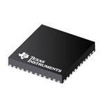
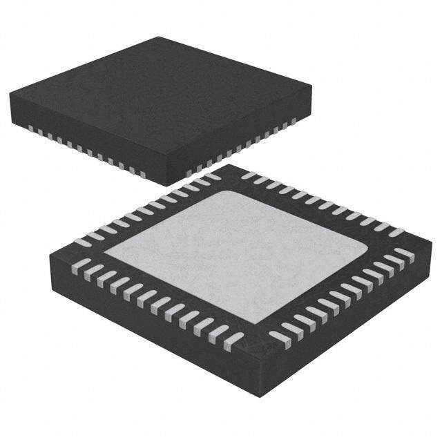
| 描述 | IC QUADRATURE MODULATOR 48VQFN调节器/解调器 300MHz to 4.8GHz Quad Modulator |
| 产品分类 | |
| LO频率 | 300MHz ~ 4.8GHz |
| 品牌 | Texas Instruments |
| 产品手册 | |
| 产品图片 |
|
| rohs | 符合RoHS无铅 / 符合限制有害物质指令(RoHS)规范要求 |
| 产品系列 | RF集成电路,调节器/解调器,Texas Instruments TRF372017IRGZT- |
| 数据手册 | 点击此处下载产品Datasheethttp://www.ti.com/lit/pdf/slyb174 |
| P1dB | 12dBm |
| 产品型号 | TRF372017IRGZT |
| PCN封装 | |
| PCN设计/规格 | |
| RF频率 | 300MHz ~ 4.8GHz |
| 产品种类 | 调节器/解调器 |
| 其它名称 | 296-27805-6 |
| 制造商产品页 | http://www.ti.com/general/docs/suppproductinfo.tsp?distId=10&orderablePartNumber=TRF372017IRGZT |
| 功能 | 升频器 |
| 包装 | Digi-Reel® |
| 商标 | Texas Instruments |
| 安装风格 | SMD/SMT |
| 封装 | Reel |
| 封装/外壳 | 48-VFQFN 裸露焊盘 |
| 封装/箱体 | VQFN-48 |
| 工厂包装数量 | 250 |
| 本底噪声 | -153dBm/Hz |
| 标准包装 | 1 |
| 测试频率 | 2.7GHz |
| 电压-电源 | 3 V ~ 3.6 V,4.5 V ~ 5.5 V |
| 电流-电源 | 200mA |
| 系列 | TRF372017 |
| 输出功率 | 3dBm |


- 商务部:美国ITC正式对集成电路等产品启动337调查
- 曝三星4nm工艺存在良率问题 高通将骁龙8 Gen1或转产台积电
- 太阳诱电将投资9.5亿元在常州建新厂生产MLCC 预计2023年完工
- 英特尔发布欧洲新工厂建设计划 深化IDM 2.0 战略
- 台积电先进制程称霸业界 有大客户加持明年业绩稳了
- 达到5530亿美元!SIA预计今年全球半导体销售额将创下新高
- 英特尔拟将自动驾驶子公司Mobileye上市 估值或超500亿美元
- 三星加码芯片和SET,合并消费电子和移动部门,撤换高东真等 CEO
- 三星电子宣布重大人事变动 还合并消费电子和移动部门
- 海关总署:前11个月进口集成电路产品价值2.52万亿元 增长14.8%


PDF Datasheet 数据手册内容提取
Product Sample & Technical Tools & Support & Folder Buy Documents Software Community TRF372017 SLWS224E–AUGUST2010–REVISEDJANUARY2016 TRF372017 Integrated IQ Modulator PLL/VCO 1 Features 3 Description • FullyIntegratedPLL/VCOandIQModulator TRF372017 is a high-performance, direct up- 1 conversion device, integrating a high-linearity, low- • LOFrequencyfrom300MHzto4.8GHz noise IQ modulator and an integer-fractional • 76-dBcSingle-CarrierWCDMAACPRat –8-dBm PLL/VCO. The VCO uses integrated frequency ChannelPower dividerstoachieveawide,continuoustuningrangeof • OIP3of26dBm 300 MHz to 4800 MHz. The LO is available as an output with independent frequency dividers. The • P1dBof11.5dBm device also accepts input from an external LO or • Integer/FractionalPLL VCO. The modulator baseband inputs can be biased • PhaseNoise–132dBc/Hz either internally or externally. Internal DC offset (at1MHz,f of2.3GHz) adjustment enables carrier cancellation. The device is VCO controlled through a 3-wire serial programming • LowNoiseFloor:–160dBm/Hz interface (SPI). A control pin invokes power-save • InputReferenceFrequencyRange:Upto mode to reduce power consumption while keeping 160MHz theVCOlockedforfaststart-up. • VCOFrequencyDividedby1-2-4-8Output DeviceInformation(1) 2 Applications PARTNUMBER PACKAGE BODYSIZE(NOM) TRF372017 VQFN(48) 7.00mm×7.00mm • WirelessInfrastructure – CDMA:IS95,UMTS,CDMA2000,TD-SCDMA (1) For all available packages, see the orderable addendum at theendofthedatasheet. – TDMA:GSM,IS-136,EDGE/UWC-136 – LTE • WirelessLocalLoop • Point-to-PointWirelessAccess • WirelessMANWidebandTransceivers spacing BlockDiagram EXT_VCO VTUNE LO_OUT BBQ FSroPmI VcmD/A Div1/2/4/8 CP_OUT Charge Pump Poly- Phase PFD Div2/ S RFOUT 4/8 DCALTLAKE SerialInterface RFDivider FSroPmI LD Lockdet RDiv PrescalerN-Dividerdivp/p+1 FSroPSDmIFromSPIcontrol PwrsaveFSroPmI VcmD/A VCCs GNDs REFIN PS BBI 1 An IMPORTANT NOTICE at the end of this data sheet addresses availability, warranty, changes, use in safety-critical applications, intellectualpropertymattersandotherimportantdisclaimers.PRODUCTIONDATA.
TRF372017 SLWS224E–AUGUST2010–REVISEDJANUARY2016 www.ti.com Table of Contents 1 Features.................................................................. 1 7.4 DeviceFunctionalModes........................................33 2 Applications........................................................... 1 7.5 RegisterMaps.........................................................34 3 Description............................................................. 1 8 ApplicationandImplementation........................ 46 4 RevisionHistory..................................................... 2 8.1 ApplicationInformation............................................46 8.2 TypicalApplication .................................................46 5 PinConfigurationandFunctions......................... 3 9 PowerSupplyRecommendations...................... 50 6 Specifications......................................................... 5 10 Layout................................................................... 51 6.1 AbsoluteMaximumRatings......................................5 6.2 RecommendedOperatingConditions.......................5 10.1 LayoutGuidelines.................................................51 6.3 ThermalInformation..................................................5 10.2 LayoutExample....................................................51 6.4 ElectricalCharacteristics...........................................6 11 DeviceandDocumentationSupport................. 52 6.5 TimingRequirements-SPI:WritingPhase..............8 11.1 DeviceSupport......................................................52 6.6 TimingRequirements-SPI:Read-BackPhase........8 11.2 CommunityResources..........................................52 6.7 TypicalCharacteristics............................................10 11.3 Trademarks...........................................................52 7 DetailedDescription............................................ 23 11.4 ElectrostaticDischargeCaution............................52 7.1 Overview.................................................................23 11.5 Glossary................................................................52 7.2 FunctionalBlockDiagram.......................................23 12 Mechanical,Packaging,andOrderable Information........................................................... 52 7.3 FeatureDescription.................................................23 4 Revision History NOTE:Pagenumbersforpreviousrevisionsmaydifferfrompagenumbersinthecurrentversion. ChangesfromRevisionD(September2013)toRevisionE Page • AddedFeatureDescriptionsection,DeviceFunctionalModessection,ApplicationandImplementationsection, PowerSupplyRecommendationssection,Layoutsection,DeviceandDocumentationSupportsection,and Mechanical,Packaging,andOrderableInformationsection.................................................................................................. 1 ChangesfromRevisionC(May2012)toRevisionD Page • ChangedtextstringfromReg1,B[30..28]=[000]toReg0,B[30..28]=[000]intheDescriptioncolumnassociated withRB_REG<0>,RB_REG<1>,andRB_REG<2>............................................................................................................ 44 ChangesfromRevisionB(March2012)toRevisionC Page • AddedgraphtitlestoFigure56and57thatweremissinginRevisionB............................................................................. 17 ChangesfromRevisionA(August2010)toRevisionB Page • DeletedCommentscolumnfromTable1............................................................................................................................... 8 • ChangedFigures12throughFigure27............................................................................................................................... 10 • ChangedthetextunderIntegerandFractionalModeSelectionthroughPracticalLimitonMaximumPFDFrequency.....23 • ChangedRDIV=20toRDIV=2inSetupExampleforFractionalMode............................................................................ 26 • ChangedRecommendedValueofEN_LD_ISOURCEfrom1to0inTable1..................................................................... 27 • ChangedcolumnheadingfromDefaultValuetoResetValueinregistertables1,2,3,4,5,6,and7............................... 34 • Addedrecommendedprogramming[xx]tovariousDescriptionstatementsinregistertables2,5,6,and7...................... 37 • ChangedRegister4,Bit21/Bit22DescriptionstatementfromOfftoNormal....................................................................... 39 • ChangedColumnheadingfromDefaultValuetoResetValueinReadbackmodesection,Register0.............................. 43 • ChangedBit5namefromCHIP_IDtoCHIP_ID_0andchangedBit6namefromNUtoCHIP_ID_1,ResetValueto1....44 • ChangedimageinFigure87. .............................................................................................................................................. 48 • ChangedthetextintheApplicationLayout,andaddedlinktoFigure95............................................................................ 51 2 SubmitDocumentationFeedback Copyright©2010–2016,TexasInstrumentsIncorporated
TRF372017 www.ti.com SLWS224E–AUGUST2010–REVISEDJANUARY2016 5 Pin Configuration and Functions RGZPackage 48-PinVQFN TopView SCAN_EN CLK DATA LE GND REFIN GND VCC_PLL CP_OUT GND VTUNE GND 8 7 6 5 4 3 2 1 0 9 8 7 4 4 4 4 4 4 4 4 4 3 3 3 PS 1 36 EXT_VCO RDBK 2 35 VCC_VCO1 VCC_DIG 3 34 LO_OUT_P GND_DIG 4 33 LO_OUT_N LD 5 32 VCC_VCO2 GND 6 31 GND VCC_LO1 7 30 VCC_LO2 GND 8 29 GND BBQ_N 9 28 BBI_N BBQ_P 10 27 BBI_P GND 11 26 GND GND 12 25 GND 3 4 5 6 7 8 9 0 1 2 3 4 1 1 1 1 1 1 1 2 2 2 2 2 D D D D D T D S X D D D GN RSV GN GN GN RFOU GN CC_D2 CC_MI GN GN GN V V PinFunctions PIN I/O DESCRIPTION NAME NO. Base-bandin-phaseinput:positiveterminal.Internal5kΩtoVCMgenerator.IfVCMis BBI_P 27 I internallygenerated(PWD_BB_VCM=0),externalACcouplingcapsand100-Ωdifferential terminationtoBBI_Nisrequired. Base-bandin-phaseinput:negativeterminal.Internal5kΩtoVCMgenerator.IfVCMis BBI_N 28 I internallygenerated(PWD_BB_VCM=0),externalACcouplingcapsand100-Ωdifferential terminationtoBBI_Pisrequired. Base-bandin-quadratureinput:negativeterminal.Internal5kΩtoVCMgenerator.IfVCMis BBQ_N 9 I internallygenerated(PWD_BB_VCM=0),externalACcouplingcapsand100-Ωdifferential terminationtoBBQ_Pisrequired. Base-bandin-quadratureinput:positiveterminal.Internal5kΩtoVCMgenerator.IfVCMis BBQ_P 10 I internallygenerated(PWD_BB_VCM=0),externalACcouplingcapsand100-Ωdifferential terminationtoBBQ_Nisrequired. CLK 47 I SPIclockinput.Digitalinput.Highimpedance. CP_OUT 40 O Chargepumpoutput DATA 46 I SPIdatainput.Digitalinput.Highimpedance. EXT_VCO 36 I Externallocaloscillatorinput.Highimpedance.NormallyAC-coupled. 6,8,11,12,13, 15,16,17,19, GND 22,23,24,25, — Ground 26,29,31,37, 39,42,44 GND_DIG 4 — Digitalground PLLlockdetectoutput,asconfiguredbyMUX_CTRL.Digitaloutputpinscansourceorsink LD 5 O upto8mAofcurrent. LE 45 I SPIlatchenable.Digitalinput.Highimpedance. Copyright©2010–2016,TexasInstrumentsIncorporated SubmitDocumentationFeedback 3
TRF372017 SLWS224E–AUGUST2010–REVISEDJANUARY2016 www.ti.com PinFunctions(continued) PIN I/O DESCRIPTION NAME NO. Localoscillatoroutput:negativeterminal.Opencollectoroutput.Apullupisrequired. LO_OUT_N 33 O NormallyAC-coupled. Localoscillatoroutput:positiveterminal.Opencollectoroutput.Apullupisrequired.Normally LO_OUT_P 34 O AC-coupled. PS 1 I Powersavingmodeenable(Low=normalmode;High=powersavingmode) SPIinternalregistersreadbackoutput.Digitaloutputpinscansourceorsinkupto8mAof RDBK 2 O current. REFIN 43 I Referenceclockinput.Highimpedance.NormallyAC-coupled. RFOUT 18 O RFoutput.Internallymatchedto50-Ωoutput.NormallyAC-coupled. RSVD 14 — Reserved.Normallyopen. SCAN_EN 48 I Internaltestingmodedigitalinput.Connecttogroundinnormaloperation VCC_D2S 20 — 5-Vmodulatoroutputbufferpowersupply VCC_DIG 3 — 3.3-Vdigitalpowersupply VCC_LO1 7 — 3.3-VTxpathlocaloscillatorchainpowersupply VCC_LO2 30 — 3.3-Voutputlocaloscillatorchainpowersupply VCC_MIX 21 — 5-Vmodulatorpowersupply VCC_PLL 41 — 3.3-VPLLpowersupply VCC_VCO1 35 — 3.3-VVCOpowersupply VCC_VCO2 32 — 3.3-Vto5-VVCOpowersupply VTUNE 38 I VCOcontrolvoltageinput 4 SubmitDocumentationFeedback Copyright©2010–2016,TexasInstrumentsIncorporated
TRF372017 www.ti.com SLWS224E–AUGUST2010–REVISEDJANUARY2016 6 Specifications 6.1 Absolute Maximum Ratings overoperatingfree-airtemperaturerange(unlessotherwisenoted)(1)(2) MIN MAX UNIT Supplyvoltage(3) –0.3 5.5 V DigitalI/Ovoltage –0.3 V +0.5 V CC T Operatingvirtualjunctiontemperature –40 150 °C J T Operatingambienttemperature –40 85 °C A T Storagetemperature –40 150 °C stg (1) StressesbeyondthoselistedunderAbsoluteMaximumRatingsmaycausepermanentdamagetothedevice.Thesearestressratings only,whichdonotimplyfunctionaloperationofthedeviceattheseoranyotherconditionsbeyondthoseindicatedunderRecommended OperatingConditions.Exposuretoabsolute-maximum-ratedconditionsforextendedperiodsmayaffectdevicereliability. (2) ESDratingnotvalidforRFsensitivepins. (3) Allvoltagevaluesarewithrespecttonetworkgroundterminal. 6.2 Recommended Operating Conditions MIN NOM MAX UNIT V 5-Vpowersupplyvoltage 4.5 5 5.5 V CC5V V 3.3-Vpowersupplyvoltage 3 3.3 3.6 V CC3V VCC_VCO2 3.3-Vto5-Vpowersupplyvoltage 3 3.3 5.5 V T Operatingambienttemperature –40 85 °C A T Operatingvirtualjunctiontemperature –40 125 °C J 6.3 Thermal Information TRF372017 THERMALMETRIC(1) RGZ(VQFN) UNIT 48PINS R Junction-to-ambientthermalresistance 30.0 °C/W θJA R Junction-to-case(top)thermalresistance 10.0 °C/W θJC(top) R Junction-to-boardthermalresistance 8.0 °C/W θJB ψ Junction-to-topcharacterizationparameter 0.5 °C/W JT ψ Junction-to-boardcharacterizationparameter 7.0 °C/W JB R Junction-to-case(bottom)thermalresistance 0.5 °C/W θJC(bot) (1) Formoreinformationabouttraditionalandnewthermalmetrics,seetheSemiconductorandICPackageThermalMetricsapplication report,SPRA953. Copyright©2010–2016,TexasInstrumentsIncorporated SubmitDocumentationFeedback 5
TRF372017 SLWS224E–AUGUST2010–REVISEDJANUARY2016 www.ti.com 6.4 Electrical Characteristics V =5V,V =3.3V,VCC_VCO2=3.3V,T =25°C,internalLO,internalVCM(unlessotherwisenoted) CC5V CC3V A PARAMETER TESTCONDITIONS MIN TYP MAX UNIT DCPARAMETERS 3.3-Vpowersupply,LOon 200 250 mA ICC Totalsupplycurrent,LOon(1) 5-Vpowersupply,LOon 117 148 mA VCC_DIG,LOon 3 5 mA VCC_LO1andVCC_LO2 121 130 mA VCC_D2S 43 60 mA VCC_MIX 74 90 mA Supplycurrent,LOon(1) VCC_VCO1 20 28 mA VCC_VCO2 17 20 LO_OUT_NandLO_OUT_P 17 28 mA VCC_PLL 24 40 mA 3.3-Vpowersupply,LOoff 165 204 mA Totalsupplycurrent,LOoff(1) 5-Vpowersupply,LOoff 117 149 mA 3.3-Vpowersupply,PSon 65 94 mA Totalsupplycurrent,PSon(1) 5-Vpowersupply,PSon 51 73 mA BASEBANDINPUTS Externallygenerated 1.7 V Vcm IandQinputDCcommonvoltage(2) Setinternally 1.6 1.7 1.85 V BW 1-dBinputfrequencybandwidth 1000 MHz Resistance 5 kΩ ZI InputImpedance ParallelCapacitance 3 pF BASEBANDINPUTDCOFFSETCONTROLD/A(3) Numberofbits ProgrammedthroughSPI 8 |BBI_P-BBI_N|or|BBQ_P-BBQ_N|,100-Ω ProgrammableDCoffsetsetting 0.02 V differentialload DIGITALINTERFACE VIH High-levelinputvoltage 2 3.3 V VIL Low-levelinputvoltage 0 0.8 V VOH High-leveloutputvoltage ReferencedtoVCC_DIG 0.8×Vcc V VOL Low-leveloutputvoltage ReferencedtoVCC_DIG 0.2×Vcc V REFERENCEOSCILLATORPARAMETERS Fref Referencefrequency 160 MHz Referenceinputsensitivity 0.2 3.3 Vp-p Parallelcapacitance 5 pF Referenceinputimpedance Parallelresistance 3900 Ω PFDCHARGEPUMP PFDfrequency(4) 100 MHz ICP Chargepumpcurrent SPIprogrammable 1.94 mA IQMODULATOROUTPUT,FLO=750MHz OutputRMSvoltageoverseinputI(orQ)RMS G Voltagegain –4 –3.2 –2.4 dB voltage P1dB Outputcompressionpoint 11 dBm IP3 OutputIP3 2inputtonesat4.5and5.5MHz 26 dBm IP2 OutputIP2 2inputtonesat4.5and5.5MHz 56.5 dBm Carrierfeedthrough Unadjusted –43.5 dBm Sidebandsuppression Unadjusted –46 dBc Outputreturnloss 10 dB (1) Maximumcurrentisworst-caseovervoltage,temperature,andexpectedprocessvariations. (2) TheTRF372017cangeneratetheinputcommonvoltageinternallyorcanacceptanexternalcommonmodevoltage.Thetwomodes areselectablethroughSPI. (3) Whentheinternalinputcommonmodevoltageisselected,itispossibletoapplysomeDCoffsetwiththeintegratedD/A. (4) SeeApplicationInformationfordiscussiononselectionofPFDfrequency. 6 SubmitDocumentationFeedback Copyright©2010–2016,TexasInstrumentsIncorporated
TRF372017 www.ti.com SLWS224E–AUGUST2010–REVISEDJANUARY2016 Electrical Characteristics (continued) V =5V,V =3.3V,VCC_VCO2=3.3V,T =25°C,internalLO,internalVCM(unlessotherwisenoted) CC5V CC3V A PARAMETER TESTCONDITIONS MIN TYP MAX UNIT Outputnoise DConlytoBBinputs;13-MHzoffsetfromLO;Pout –162 dBm/Hz =–10dBm IQMODULATOROUTPUT,FLO=900MHz OutputRMSvoltageoverseinputI(orQ)RMS G Voltagegain –4 –3.4 –2.4 dB voltage P1dB Outputcompressionpoint 11 dBm IP3 OutputIP3 2inputtonesat4.5and5.5MHz 26.5 dBm IP2 OutputIP2 2inputtonesat4.5and5.5MHz 56.5 dBm Carrierfeedthrough Unadjusted –43 dBm Sidebandsuppression Unadjusted –45 dBc Outputreturnloss 10 dB Outputnoise DConlytoBBinputs;13-MHzoffsetfromLO;Pout –160 dBm/Hz =–10dBm IQMODULATOROUTPUT,FLO=2150MHz OutputRMSvoltageoverseinputI(orQ)RMS G Voltagegain –4.2 –3.1 –2 dB voltage P1dB Outputcompressionpoint 11.5 dBm IP3 OutputIP3 2inputtonesat4.5and5.5MHz 25 dBm IP2 OutputIP2 2inputtonesat4.5and5.5MHz 56 dBm Carrierfeedthrough Unadjusted –40 dBm Sidebandsuppression Unadjusted –32 dBc Outputreturnloss 10 dB Outputnoise DConlytoBBinputs;13-MHzoffsetfromLO;Pout –158 dBm/Hz =–10dBm 1WCDMAsignal;Pout=–8dBm –75 ACPR Adjacent-channelpowerratio dBc 2WCDMAsignals;Pout=–11dBmpercarrier 71 IQMODULATOROUTPUT,FLO=2700MHz OutputRMSvoltageoverseinputI(orQ)RMS G Voltagegain –4.1 –2.7 –1.3 dB voltage P1dB Outputcompressionpoint 12 dBm IP3 OutputIP3 2inputtonesat4.5and5.5MHz 26.5 dBm IP2 OutputIP2 2inputtonesat4.5and5.5MHz 50 dBm Carrierfeedthrough Unadjusted –43 dBm Sidebandsuppression Unadjusted –41 dBc Outputreturnloss 10 dB Outputnoise DConlytoBBinputs;13-MHzoffsetfromLO;Pout –153 dBm/Hz =–10dBm LOCALOSCILLATOR VCOrange 2400 4800 Divideby2 1200 2400 FVCO Frequencyrange MHz Divideby4 600 1200 Divideby8 300 600 FreerunningVCO 10kHz –85 dBc/Hz Phasenoise,Fout=2.3GHz 1MHz –132 dBc/Hz 10MHz –150 dBc/Hz 50MHz –153 dBc/Hz PLO LOoutputpower(5) 100-Ωdifferential,externalload;single-ended –2.5 3 dBm (5) WithVCOfrequencyat4.6GHzandLOindivide-by-2modeat2.3GHz Copyright©2010–2016,TexasInstrumentsIncorporated SubmitDocumentationFeedback 7
TRF372017 SLWS224E–AUGUST2010–REVISEDJANUARY2016 www.ti.com 6.5 Timing Requirements - SPI: Writing Phase(1) MIN TYP MAX UNIT t Holdtime,datatoclock 20 ns h t Setuptime,datatoclock 20 ns SU1 T Clocklowduration 20 ns (CH) T Clockhighduration 20 ns (CL) t Setuptime,clocktoenable 20 ns SU2 t Clockperiod 50 ns (CLK) t Enabletime 50 ns W t Setuptime,latchtodata 70 ns SU3 (1) SeeFigure1fortimingdiagram. 6.6 Timing Requirements - SPI: Read-Back Phase(1) MIN TYP MAX UNIT t Holdtime,datatoclock 20 ns h t Setuptime,datatoclock 20 ns SU1 T Clocklowduration 20 ns (CH) T ClockHighduration 20 ns (CL) t Setuptime,clocktoenable 20 ns SU2 t Delaytime,clocktoreadbackdataoutput 10 ns d t Enabletime(2) 50 ns W t Clockperiod 50 ns (CLK) (1) SeeFigure2fortimingdiagram. (2) EqualsClockperiod t tsu1 th t(CLK) (CL) t(CH) CLOCK 1stWrite 32nd clock Write E pulse clock T pulse RI W ER ADdBdr0es(LsS BBit)0 AddrDeBss1 Bit1 AddrDeBss2 Bit2 AddrDeBss3 Bit3 DB29 DB30 DB31(MSB) T DATA GIS tsu3 tsu2 tw E R LATCH End ofWrite Cycle pulse ENABLE Figure1. SPIWriteTimingDiagram 8 SubmitDocumentationFeedback Copyright©2010–2016,TexasInstrumentsIncorporated
TRF372017 www.ti.com SLWS224E–AUGUST2010–REVISEDJANUARY2016 tsu1 th t(CLK) T(CL) 1sctlWocrkite T(CH) 32ndWrite pulse clock pulse CLOCK E T WRI ADdBd0re(sLsS BBi)t0 AddDreBs1s Bit1 AddDreBs2s Bit2 AddDreBs3s Bit3 DB29 DB30 DB31(MSB) R DATA E T S GI E R LATCH ENABLE 32nd Write tsu3 1stRead 2ndRead 32ndRead 33rdRead clock clock pulse clock pulse clock pulse clock pulse CLOCK pulse t su2 K C “End of Write Cycle” A pulse td DB LATCH ENABLE tw A E Read Read R ReadBack Back Back ReadBack ReadBack Data Bit0 Data Data Data Bit30 Data Bit31 READBACK DATA Bit1 Bit29 Figure2. SPIRead-BackTimingDiagram Copyright©2010–2016,TexasInstrumentsIncorporated SubmitDocumentationFeedback 9
TRF372017 SLWS224E–AUGUST2010–REVISEDJANUARY2016 www.ti.com 6.7 Typical Characteristics V =1.7V(internal),V =300mVrmssingle-endedsinewaveinquadrature,V =3.3V,V =5V,f =4.5MHz CM inBB CC3V CC5V BB and5.5MHz,internalLO,T =25°C;F =1.6MHz(unlessotherwisenoted). A PFD -40 -40 F_LO_OUT= 2.6 GHz F_LO_OUT= 3.35 GHz VCC= 3.3, 5 V VCC= 3.3, 5 V -60 -60 Noise(dBc/Hz) -1-8000 TA= 85°C Noise(dBc/Hz) -1-8000 TA= 85°C Phase -120 Phase -120 TA= -40°C TA= -40°C -140 -140 TA= 25°C TA= 25°C -160 -160 1k 10k 100k 1M 10M 40M 1k 10k 100k 1M 10M 40M Frequency (Hz) Frequency (Hz) G001 G002 Figure3.Open-LoopPhaseNoise Figure4.OpenLoopPhaseNoise vsFrequencyandTemperature vsFrequencyandTemperature -40 -40 F_LO_OUT= 4.05 GHz F_LO_OUT= 4.7 GHz VCC= 3.3, 5 V VCC= 3.3, 5 V -60 -60 Bc/Hz) -80 TA= 85°C Bc/Hz) -80 TA= 85°C Noise(d -100 Noise(d -100 Phase -120 Phase -120 TA= -40°C TA= -40°C -140 TA= 25°C -140 TA= 25°C -160 -160 1k 10k 100k 1M 10M 40M 1k 10k 100k 1M 10M 40M Frequency (Hz) Frequency (Hz) G003 G004 Figure5.OpenLoopPhaseNoise Figure6.OpenLoopPhaseNoise vsFrequencyandTemperature vsFrequencyandTemperature -40 -40 F_LO_OUT= 2.6 GHz F_LO_OUT= 3.35 GHz TA= 25°C TA= 25°C -60 -60 Hz) -80 Hz) -80 Noise(dBc/ -100 VCC= 3.6 V Noise(dBc/ -100 VCC= 3.6 V Phase -120 Phase -120 VCC= 3 V VCC= 3 V -140 -140 VCC= 3.3 V VCC= 3.3 V -160 -160 1k 10k 100k 1M 10M 40M 1k 10k 100k 1M 10M 40M Frequency (Hz) Frequency (Hz) G005 G006 Figure7.OpenLoopPhaseNoise Figure8.OpenLoopPhaseNoise vsFrequencyandSupplyVoltage vsFrequencyandSupplyVoltage 10 SubmitDocumentationFeedback Copyright©2010–2016,TexasInstrumentsIncorporated
TRF372017 www.ti.com SLWS224E–AUGUST2010–REVISEDJANUARY2016 Typical Characteristics (continued) V =1.7V(internal),V =300mVrmssingle-endedsinewaveinquadrature,V =3.3V,V =5V,f =4.5MHz CM inBB CC3V CC5V BB and5.5MHz,internalLO,T =25°C;F =1.6MHz(unlessotherwisenoted). A PFD -40 -40 F_LO_OUT= 4.05 GHz F_LO_OUT= 4.7 GHz TA= 25°C TA= 25°C -60 -60 VCC= 3 V VCC= 3 V Hz) -80 Hz) -80 Bc/ Bc/ Noise(d -100 Noise(d -100 Phase -120 VCC= 3.3 V VCC= 3.6 V Phase -120 VCC= 3.3 V VCC= 3.6 V -140 -140 -160 -160 1k 10k 100k 1M 10M 40M 1k 10k 100k 1M 10M 40M Frequency (Hz) Frequency (Hz) G007 G008 Figure9.OpenLoopPhaseNoise Figure10.OpenLoopPhaseNoise vsFrequencyandSupplyVoltage vsFrequencyandSupplyVoltage -40 -40 F_LO_OUT= 2.6 GHz F_LO_OUT= 1.3 GHz VCC= 3.3, 5 V VCC= 3.3, 5 V -60 Div 1 Mode -60 Div 2 Mode Bc/Hz) -80 TA= 85°C Bc/Hz) -80 Noise (d -100 Noise (d -100 Phase -120 TA= -40°C Phase -120 TA= 85°C TA= -40°C -140 TA= 25°C -140 TA= 25°C -160 -160 1k 10k 100k 1M 10M 40M 1k 10k 100k 1M 10M 40M Frequency (Hz) Frequency (Hz) G009 G010 Figure11.ClosedLoopPhaseNoise Figure12.ClosedLoopPhaseNoise vsFrequencyandTemperature vsFrequencyandTemperature -40 -40 F_LO_OUT= 650 MHz F_LO_OUT= 325 MHz VCC= 3.3, 5 V VCC= 3.3, 5 V -60 Div 4 Mode -60 Div 8 Mode Hz) -80 Hz) -80 Bc/ Bc/ Noise (d -100 TA= 85°C Noise (d -100 TA= 25°C Phase -120 Phase -120 TA= -40°C TA= 25°C TA= 85°C -140 -140 TA= -40°C -160 -160 1k 10k 100k 1M 10M 40M 1k 10k 100k 1M 10M 40M Frequency (Hz) Frequency (Hz) G011 G012 Figure13.ClosedLoopPhaseNoise Figure14.ClosedLoopPhaseNoise vsFrequencyandTemperature vsFrequencyandTemperature Copyright©2010–2016,TexasInstrumentsIncorporated SubmitDocumentationFeedback 11
TRF372017 SLWS224E–AUGUST2010–REVISEDJANUARY2016 www.ti.com Typical Characteristics (continued) V =1.7V(internal),V =300mVrmssingle-endedsinewaveinquadrature,V =3.3V,V =5V,f =4.5MHz CM inBB CC3V CC5V BB and5.5MHz,internalLO,T =25°C;F =1.6MHz(unlessotherwisenoted). A PFD -40 -40 F_LO_OUT= 3.4 GHz F_LO_OUT= 1.7 GHz VCC= 3.3, 5 V VCC= 3.3, 5 V -60 Div 1 Mode -60 Div 2 Mode Bc/Hz) -80 TA= 85°C Bc/Hz) -80 TA= 85°C Noise (d -100 Noise (d -100 Phase -120 TA= -40°C Phase -120 TA= -40°C -140 -140 TA= 25°C TA= 25°C -160 -160 1k 10k 100k 1M 10M 40M 1k 10k 100k 1M 10M 40M Frequency (Hz) Frequency (Hz) G013 G014 Figure15.ClosedLoopPhaseNoise Figure16.ClosedLoopPhaseNoise vsFrequencyandTemperature vsFrequencyandTemperature -40 -40 F_LO_OUT= 850 MHz F_LO_OUT= 425 MHz VCC= 3.3, 5 V VCC= 3.3, 5 V -60 Div 4 Mode -60 Div 8 Mode Hz) -80 Hz) -80 Bc/ Bc/ Noise (d -100 TA= 85°C Noise (d -100 TA= 85°C Phase -120 Phase -120 TA= -40°C TA= 25°C -140 -140 TA= -40°C TA= 25°C -160 -160 1k 10k 100k 1M 10M 40M 1k 10k 100k 1M 10M 40M Frequency (Hz) Frequency (Hz) G015 G016 Figure17.ClosedLoopPhaseNoise Figure18.ClosedLoopPhaseNoise vsFrequencyandTemperature vsFrequencyandTemperature -40 -40 F_LO_OUT= 4 GHz F_LO_OUT= 2 GHz VCC= 3.3, 5 V VCC= 3.3, 5 V -60 Div 1 Mode -60 Div 2 Mode Bc/Hz) -80 TA= 85°C Bc/Hz) -80 TA= 85°C Noise (d -100 Noise (d -100 Phase -120 TA= -40°C Phase -120 TA= -40°C -140 TA= 25°C -140 TA= 25°C -160 -160 1k 10k 100k 1M 10M 40M 1k 10k 100k 1M 10M 40M Frequency (Hz) Frequency (Hz) G017 G018 Figure19.ClosedLoopPhaseNoise Figure20.ClosedLoopPhaseNoise vsFrequencyandTemperature vsFrequencyandTemperature 12 SubmitDocumentationFeedback Copyright©2010–2016,TexasInstrumentsIncorporated
TRF372017 www.ti.com SLWS224E–AUGUST2010–REVISEDJANUARY2016 Typical Characteristics (continued) V =1.7V(internal),V =300mVrmssingle-endedsinewaveinquadrature,V =3.3V,V =5V,f =4.5MHz CM inBB CC3V CC5V BB and5.5MHz,internalLO,T =25°C;F =1.6MHz(unlessotherwisenoted). A PFD -40 -40 F_LO_OUT= 1 GHz F_LO_OUT= 500 MHz VCC= 3.3, 5 V VCC= 3.3, 5 V -60 Div 4 Mode -60 Div 8 Mode Hz) -80 Hz) -80 Bc/ Bc/ Noise (d -100 TA= 85°C Noise (d -100 TA= 85°C Phase -120 TA= -40°C TA= 25°C Phase -120 TA= 25°C -140 -140 TA= -40°C -160 -160 1k 10k 100k 1M 10M 40M 1k 10k 100k 1M 10M 40M Frequency (Hz) Frequency (Hz) G019 G020 Figure21.ClosedLoopPhaseNoise Figure22.ClosedLoopPhaseNoise vsFrequencyandTemperature vsFrequencyandTemperature -40 -40 F_LO_OUT= 4.6 GHz F_LO_OUT= 2.3 GHz VCC= 3.3, 5 V VCC= 3.3, 5 V -60 Div 1 Mode -60 Div 2 Mode Bc/Hz) -80 TA= 85°C Bc/Hz) -80 TA= 85°C Noise (d -100 Noise (d -100 Phase -120 TA= -40°C Phase -120 TA= 25°C TA= -40°C -140 TA= 25°C -140 -160 -160 1k 10k 100k 1M 10M 40M 1k 10k 100k 1M 10M 40M Frequency (Hz) Frequency (Hz) G021 G022 Figure23.ClosedLoopPhaseNoise Figure24.ClosedLoopPhaseNoise vsFrequencyandTemperature vsFrequencyandTemperature -40 -40 F_LO_OUT= 1.15 GHz F_LO_OUT= 575 MHz VCC= 3.3, 5 V VCC= 3.3, 5 V -60 Div 4 Mode -60 Div 8 Mode Hz) -80 Hz) -80 Bc/ Bc/ Noise (d -100 TA= 85°C Noise (d -100 TA= 85°C Phase -120 Phase -120 TA= -40°C TA= 25°C TA= -40°C TA= 25°C -140 -140 -160 -160 1k 10k 100k 1M 10M 40M 1k 10k 100k 1M 10M 40M Frequency (Hz) Frequency (Hz) G023 G024 Figure25.ClosedLoopPhaseNoise Figure26.ClosedLoopPhaseNoise vsFrequencyandTemperature vsFrequencyandTemperature Copyright©2010–2016,TexasInstrumentsIncorporated SubmitDocumentationFeedback 13
TRF372017 SLWS224E–AUGUST2010–REVISEDJANUARY2016 www.ti.com Typical Characteristics (continued) V =1.7V(internal),V =300mVrmssingle-endedsinewaveinquadrature,V =3.3V,V =5V,f =4.5MHz CM inBB CC3V CC5V BB and5.5MHz,internalLO,T =25°C;F =1.6MHz(unlessotherwisenoted). A PFD -130 -130 VCC= 3.3, 5 V TA= 25°C Internal VCO Internal VCO -140 PO= -10 dBm -140 PO= -10dBm Hz) TA= 85°C Hz) VCC= 3 V Bm/ -150 Bm/ -150 HzOffset (d -160 HzOffset (d -160 VCC= 3.3 V at13-M -170 TA= -40°C TA= 25°C at13-M -170 VCC= 3.6 V Noise Noise -180 -180 -190 -190 350 700 1050 1400 1750 2100 2450 2800 3150 3500 350 700 1050 1400 1750 2100 2450 2800 3150 3500 Frequency (MHz) Frequency (MHz) G025 G026 Figure27.Noiseat13-MHzOffset Figure28.Noiseat13-MHzOffset vsFrequencyandTemperatureWithInternalVCO vsFrequencyandSupplyVoltageWithInternalVCO -130 -130 VCC= 3.3, 5 V TA= 25°C External VCO External VCO -140 PO= -10dBm -140 PO= -10dBm Hz) TA= 85°C Hz) VCC= 3.3 V Bm/ -150 Bm/ -150 at13-MHzOffset (d --117600 TA= -40°C TA= 25°C at13-MHzOffset (d --117600 VCC= 3 V VCC= 3.6 V Noise Noise -180 -180 -190 -190 350 700 1050 1400 1750 2100 2450 2800 3150 3500 350 700 1050 1400 1750 2100 2450 2800 3150 3500 Frequency (MHz) Frequency (MHz) G027 G028 Figure29.Noiseat13-MHzOffset Figure30.Noiseat13-MHzOffset vsFrequencyandTemperatureWithExternalVCO vsFrequencyandSupplyVoltageWithExternalVCO -130 2 VCC= 3.3, 5 V -135 TA= 25°C f = 2140 MHz 1 -140 f = 3500 MHz Hz) f = 2700 MHz 0 m/ -145 B -1 at13-MHzOffset (d ---111655050 f = 900 MHz Voltage Gain (dB) ---432 TA= -40°CTA= 25°C Noise -165 f = 750 MHz -5 -170 f = 450 MHz TA= 85°C -175 -6 -180 -7 -15 -10 -5 0 5 10 300 800 1300 1800 2300 2800 3300 3800 4300 4800 Output Power (dBm) Frequency (MHz) G029 G030 Figure31.Noiseat13-MHzOffset Figure32.VoltageGainvsFrequencyandTemperature vsOutputPowerandFrequency 14 SubmitDocumentationFeedback Copyright©2010–2016,TexasInstrumentsIncorporated
TRF372017 www.ti.com SLWS224E–AUGUST2010–REVISEDJANUARY2016 Typical Characteristics (continued) V =1.7V(internal),V =300mVrmssingle-endedsinewaveinquadrature,V =3.3V,V =5V,f =4.5MHz CM inBB CC3V CC5V BB and5.5MHz,internalLO,T =25°C;F =1.6MHz(unlessotherwisenoted). A PFD -3 -3.2 TA= 25°C -3.25 -3.1 -3.3 TA= -40°C Gain (dB) -3.2 TA= -40°C Gain (dB) -3-3.3.45 Voltage -3.3 Voltage -3.45 TA= 25°C TA= 85°C -3.5 -3.4 -3.55 TA= 85°C -3.5 -3.6 720 725 730 735 740 745 750 755 760 765 770 880 885 890 895 900 905 910 915 920 Frequency (MHz) Frequency (MHz) G031 G032 Figure33.VoltageGain Figure34.VoltageGain vsFrequencyandTemperatureat750MHz vsFrequencyandTemperatureat900MHz -3.6 -3.4 -3.5 -3.7 -3.6 -3.8 TA= -40°C -3.7 TA= -40°C Gain (dB) -3.9 Gain (dB) --33..98 Voltage -4 TA= 25°C Voltage -4 -4.1 -4.1 -4.2 TA= 85°C -4.2 TA= 25°C TA= 85°C -4.3 -4.3 -4.4 1465 1470 1475 1480 1485 1490 1495 1500 1505 1510 2100 2110 2120 2130 2140 2150 2160 2170 Frequency (MHz) Frequency (MHz) G033 G034 Figure35.VoltageGain Figure36.VoltageGain vsFrequencyandTemperatureat1500MHz vsFrequencyandTemperatureat2150MHz -2.7 -2.4 -2.6 f = 2700 MHz -2.8 TA= -40°C -2.8 -2.9 TA= 25°C -3 f = 750 MHz Gain (dB) -3-.31 Gain (dB) --33..42 f = 900 MHz Voltage -3.2 Voltage -3.6 f = 2150 MHz -3.8 -3.3 TA= 85°C -4 -3.4 -4.2 f = 1500 MHz -3.5 -4.4 2610 2620 2630 2640 2650 2660 2670 2680 2690 1.55 1.6 1.65 1.7 1.75 1.8 1.85 1.9 Frequency (MHz) Common-Mode Voltage (V) G035 G036 Figure37.VoltageGain Figure38.VoltageGain vsFrequencyandTemperatureat2650MHz vsCommon-ModeVoltageandFrequency Copyright©2010–2016,TexasInstrumentsIncorporated SubmitDocumentationFeedback 15
TRF372017 SLWS224E–AUGUST2010–REVISEDJANUARY2016 www.ti.com Typical Characteristics (continued) V =1.7V(internal),V =300mVrmssingle-endedsinewaveinquadrature,V =3.3V,V =5V,f =4.5MHz CM inBB CC3V CC5V BB and5.5MHz,internalLO,T =25°C;F =1.6MHz(unlessotherwisenoted). A PFD -2.5 1 f = 2700 MHz -2.7 0 -2.9 f = 750 MHz -3.1 -1 Gain (dB) --33..53 f = 900 MHz Gain (dB) -2 Voltage -3.7 f = 2150 MHz Voltage VCC= 3.3 V -3 -3.9 VCC= 3.6 V -4.1 -4 f = 1500 MHz -4.3 BB Voltage is Single-Ended RMS VCC= 3 V -4.5 -5 0 100 200 300 400 500 600 700 800 900 1000 300 800 1300 1800 2300 2800 3300 3800 4300 4800 Baseband VoltageAmplitude (mV) Frequency (MHz) G037 G038 Figure39.VoltageGain Figure40.VoltageGainvsFrequencyandSupplyVoltage vsBasebandVoltageAmplitudeandFrequency 15 11.3 14 11.2 TA= 25°C 13 TA= 25°C 11.1 12 11 m) 11 m) TA= 85°C B B B(d 10 TA= 85°C B(d 10.9 P1d 9 TA= -40°C P1d 10.8 8 10.7 7 TA= -40°C 10.6 6 5 10.5 300 800 1300 1800 2300 2800 3300 3800 4300 4800 700 710 720 730 740 750 760 770 780 790 800 Frequency (MHz) Frequency (MHz) G039 G040 Figure41.P1dBvsFrequencyandTemperature Figure42.P1dBvsFrequencyandTemperatureat750MHz 11.4 11.5 11.3 TA= 25°C 11.4 TA= 25°C 11.3 11.2 11.2 11.1 Bm) 11 Bm) 11.1 P1dB(d 10.9 TA= 85°C P1dB(d 101.19 TA= 85°C 10.8 TA= -40°C 10.8 10.7 10.7 10.6 TA= -40°C 10.6 10.5 10.5 850 860 870 880 890 900 910 920 930 940 950 14501460147014801490150015101520153015401550 Frequency (MHz) Frequency (MHz) G041 G042 Figure43.P1dBvsFrequencyandTemperatureat900MHz Figure44.P1dBvsFrequencyandTemperatureat1500MHz 16 SubmitDocumentationFeedback Copyright©2010–2016,TexasInstrumentsIncorporated
TRF372017 www.ti.com SLWS224E–AUGUST2010–REVISEDJANUARY2016 Typical Characteristics (continued) V =1.7V(internal),V =300mVrmssingle-endedsinewaveinquadrature,V =3.3V,V =5V,f =4.5MHz CM inBB CC3V CC5V BB and5.5MHz,internalLO,T =25°C;F =1.6MHz(unlessotherwisenoted). A PFD 12.2 12.6 12 12.4 TA= 25°C TA= 25°C 12.2 11.8 12 m) 11.6 m) B(dB TA= -40°C B(dB 11.8 TA= -40°C P1d 11.4 P1d 11.6 11.2 11.4 11 TA= 85°C 11.2 TA= 85°C 10.8 11 21002110212021302140215021602170218021902200 26502660267026802690270027102720273027402750 Frequency (MHz) Frequency (MHz) G043 G044 Figure45.P1dBvsFrequencyandTemperatureat2150MHz Figure46.P1dBvsFrequencyandTemperatureat2700MHz 14 15 14 f = 2700 MHz 13 f = 2150 MHz 13 VCC= 3.6 V 12 12 Bm) Bm) 11 P1dB(d 11 f = 1500 MHz P1dB(d 10 VCC= 3.3 V 10 f = 900 MHz 9 VCC= 3 V 8 f = 750 MHz 9 7 8 6 1.55 1.6 1.65 1.7 1.75 1.8 1.85 1.9 300 800 1300 1800 2300 2800 3300 3800 4300 4800 Common-Mode Voltage (V) Frequency (MHz) G045 G046 Figure47.P1dBvsCommon-ModeVoltageandFrequency Figure48.P1dBvsFrequencyandSupplyVoltage 34 28 32 TA= -40°C 27.5 30 TA= 25°C 27 TA= -40°C 28 26.5 m) 26 m) B B P3 (d 24 P3 (d 26 OI 22 OI TA= 85°C TA= 25°C 25.5 20 TA= 85°C 25 18 24.5 16 14 24 300 800 1300 1800 2300 2800 3300 3800 4300 4800 880 885 890 895 900 905 910 915 920 Frequency (MHz) Frequency (MHz) G047 G048 Figure49.OIP3vsFrequencyandTemperature Figure50.OIP3vsTemperatureandFrequencyat900MHz Copyright©2010–2016,TexasInstrumentsIncorporated SubmitDocumentationFeedback 17
TRF372017 SLWS224E–AUGUST2010–REVISEDJANUARY2016 www.ti.com Typical Characteristics (continued) V =1.7V(internal),V =300mVrmssingle-endedsinewaveinquadrature,V =3.3V,V =5V,f =4.5MHz CM inBB CC3V CC5V BB and5.5MHz,internalLO,T =25°C;F =1.6MHz(unlessotherwisenoted). A PFD 28 26 27.5 TA= 25°C 25.5 TA= -40°C TA= -40°C 27 25 26.5 24.5 m) m) B B P3 (d 26 P3 (d 24 OI OI 25.5 23.5 TA= 25°C TA= 85°C 25 23 TA= 85°C 24.5 22.5 24 22 1000 1005 1010 1015 1020 1025 1030 1035 1040 16201625163016351640164516501655166016651670 Frequency (MHz) Frequency (MHz) G049 G050 Figure51.OIP3vsFrequencyandTemperatureat1030MHz Figure52.OIP3vsFrequencyandTemperatureat1650MHz 27 30 TA= -40°C 26 29 TA= 25°C 28 25 m) m) 27 OIP3 (dB 24 TA= 25°C OIP3 (dB 26 TA= -40°C 23 25 22 TA= 85°C 24 TA= 85°C 21 23 2260 2270 2280 2290 2300 2310 2320 2770 2780 2790 2800 2810 2820 2830 2840 2850 Frequency (MHz) Frequency (MHz) G051 G052 Figure53.OIP3vsFrequencyandTemperatureat2300MHz Figure54.OIP3vsFrequencyandTemperatureat2850MHz 29 30 f = 900 MHz 29 f = 900 MHz f = 2150 MHz 28 f = 2700 MHz 28 27 f = 2700 MHz 27 m) 26 m) 26 OIP3 (dB 25 f = 2150 MHz OIP3 (dB 2254 24 f = 750 MHz f = 1500 MHz 23 23 f = 1500 MHz f = 750 MHz 22 22 21 TA= 25°C BB Voltage is Single-Ended RMS 21 20 1.5 1.55 1.6 1.65 1.7 1.75 1.8 1.85 1.9 0 100 200 300 400 500 600 700 800 900 1000 Common-Mode Voltage (V) Baseband VoltageAmplitude (mV) G053 G083 Figure55.OIP3vsCommon-ModeVoltageandFrequency Figure56.OIP3vsBasebandVoltageAmplitudeand Frequency 18 SubmitDocumentationFeedback Copyright©2010–2016,TexasInstrumentsIncorporated
TRF372017 www.ti.com SLWS224E–AUGUST2010–REVISEDJANUARY2016 Typical Characteristics (continued) V =1.7V(internal),V =300mVrmssingle-endedsinewaveinquadrature,V =3.3V,V =5V,f =4.5MHz CM inBB CC3V CC5V BB and5.5MHz,internalLO,T =25°C;F =1.6MHz(unlessotherwisenoted). A PFD 70 58 65 TA= -40°C 57.5 TA= 85°C 60 57 TA= 25°C 55 m) m) B B P2 (d 50 P2 (d 56.5 OI OI 45 TA= 25°C 56 40 TA= 85°C TA= -40°C 55.5 35 30 55 300 800 1300 1800 2300 2800 3300 3800 4300 4800 730 735 740 745 750 755 760 765 770 Frequency (MHz) Frequency (MHz) G054 G055 Figure57.OIP2vsFrequencyandTemperature Figure58.OIP2vsFrequencyandTemperatureat750MHz 58 58 57.5 57.5 TA= -40°C 57 TA= 85°C 57 TA= 25°C 56.5 m) m) B B P2 (d 56.5 P2 (d 56 OI OI 55.5 56 TA= 25°C 55 55.5 TA= 85°C 54.5 TA= -40°C 55 54 880 885 890 895 900 905 910 915 920 1470 1475 1480 1485 1490 1495 1500 1505 1510 Frequency (MHz) Frequency (MHz) G056 G057 Figure59.OIP2vsFrequencyandTemperatureat900MHz Figure60.OIP2vsFrequencyandTemperatureat1500MHz 57 54 56.5 TA= -40°C 53 TA= 85°C 56 TA= 25°C 52 55.5 51 m) m) B B P2 (d 55 P2 (d 50 OI OI 54.5 49 TA= 25°C 54 TA= 85°C 48 53.5 47 TA= -40°C 53 46 2100 2110 2120 2130 2140 2150 2160 2170 2180 2620 2630 2640 2650 2660 2670 2680 2690 Frequency (MHz) Frequency (MHz) G058 G059 Figure61.OIP2vsFrequencyandTemperatureat2150MHz Figure62.OIP2vsFrequencyandTemperatureat2650MHz Copyright©2010–2016,TexasInstrumentsIncorporated SubmitDocumentationFeedback 19
TRF372017 SLWS224E–AUGUST2010–REVISEDJANUARY2016 www.ti.com Typical Characteristics (continued) V =1.7V(internal),V =300mVrmssingle-endedsinewaveinquadrature,V =3.3V,V =5V,f =4.5MHz CM inBB CC3V CC5V BB and5.5MHz,internalLO,T =25°C;F =1.6MHz(unlessotherwisenoted). A PFD 55 46.5 Suppression (dBc) 4550 TA= 85°C TA= -40°C Suppression (dBc) 46 TA= 25°C Sideband 40 Sideband TA= 85°C Unadjusted 3305 TA= 25°C Unadjusted 45.5 TA= -40°C 25 45 300 800 1300 1800 2300 2800 3300 3800 4300 4800 880 885 890 895 900 905 910 915 920 Frequency (MHz) Frequency (MHz) G060 G061 Figure63.UnadjustedSidebandSuppression Figure64.UnadjustedSidebandSuppression vsFrequencyandTemperature vsFrequencyandTemperatureat900MHz 47 43 46.5 42.5 Bc) TA= -40°C Bc) Sideband Suppression (d 444544..5655 TA= 25°C Sideband Suppression (d 440144..1255 TA= -40°C TA= 85°C Unadjusted 44 TA= 85°C Unadjusted 40 TA= 25°C 43.5 39.5 43 39 1000 1005 1010 1015 1020 1025 1030 1035 1040 1610 1620 1630 1640 1650 1660 1670 Frequency (MHz) Frequency (MHz) G062 G063 Figure65.UnadjustedSidebandSuppression Figure66.UnadjustedSidebandSuppression vsFrequencyandTemperatureat1030MHz vsFrequencyandTemperatureat1650MHz 37 44 36 Sideband Suppression (dBc) 333345 TA= 25°CTA= -40°C Sideband Suppression (dBc) 444123 TA= 85°C TA= -40°C Unadjusted 32 TA= 85°C Unadjusted 40 TA= 25°C 31 30 39 2250 2260 2270 2280 2290 2300 2310 2320 2330 2760 2770 2780 2790 2800 2810 2820 2830 2840 2850 Frequency (MHz) Frequency (MHz) G064 G065 Figure67.UnadjustedSidebandSuppression Figure68.UnadjustedSidebandSuppression vsFrequencyandTemperatureat2300MHz vsFrequencyandTemperatureat2850MHz 20 SubmitDocumentationFeedback Copyright©2010–2016,TexasInstrumentsIncorporated
TRF372017 www.ti.com SLWS224E–AUGUST2010–REVISEDJANUARY2016 Typical Characteristics (continued) V =1.7V(internal),V =300mVrmssingle-endedsinewaveinquadrature,V =3.3V,V =5V,f =4.5MHz CM inBB CC3V CC5V BB and5.5MHz,internalLO,T =25°C;F =1.6MHz(unlessotherwisenoted). A PFD 50 -21 TA= 25°C -24 48 f = 750 MHz Bc) m) -27 Sideband Suppression (d 44440246 f = 2700 MHz f = 900 MHz CarrierSuppression (dB ----33339630 TA= 25°C TA= -40°C Unadjusted 38 f = 1500 MHz Unadjusted --4452 36 f = 2150 MHz -48 TA= 85°C 34 -51 11..5555 1.6 1.65 1.7 1.75 1.8 1.85 11..99 300 800 1300 1800 2300 2800 3300 3800 4300 4800 Common-Mode Voltage (V) G066 Frequency (MHz) G067 Figure69.UnadjustedSidebandSuppression Figure70.UnadjustedCarrierSuppression vsCommon-ModeVoltageandFrequency vsFrequencyandTemperature -41 -42 -41.5 -42.5 TA= 25°C m) -42 m) Suppression (dB --44-324..355 TAT=A -=40 2°5C°C Suppression (dB -4--344.435 UnadjustedCarrier -4--444.545 TA= 85°C UnadjustedCarrier -4-44.55 TA= -40°C TA= 85°C -45.5 -45.5 -46 -46 880 885 890 895 900 905 910 915 920 990 1000 1010 1020 1030 1040 1050 Frequency (MHz) Frequency (MHz) G068 G069 Figure71.UnadjustedCarrierSuppression Figure72.UnadjustedCarrierSuppression vsFrequencyandTemperatureat900MHz vsFrequencyandTemperatureat1030MHz -43 -35 -43.5 -36 TA= -40°C UnadjustedCarriersuppression(dBm) --44---54444..65455 TA= 25°C TA= 85°C UnadjustedCarrierSuppression (dBm) -------44443333210987 TA= 25°C TA= 85°C -46.5 TA= -40°C -44 -47 -45 1610 1620 1630 1640 1650 1660 1670 2250 2260 2270 2280 2290 2300 2310 2320 2330 Frequency (MHz) Frequency (MHz) G070 G071 Figure73.UnadjustedCarrierSuppression Figure74.UnadjustedCarrierSuppression vsFrequencyandTemperatureat1650MHz vsFrequencyandTemperatureat2300MHz Copyright©2010–2016,TexasInstrumentsIncorporated SubmitDocumentationFeedback 21
TRF372017 SLWS224E–AUGUST2010–REVISEDJANUARY2016 www.ti.com Typical Characteristics (continued) V =1.7V(internal),V =300mVrmssingle-endedsinewaveinquadrature,V =3.3V,V =5V,f =4.5MHz CM inBB CC3V CC5V BB and5.5MHz,internalLO,T =25°C;F =1.6MHz(unlessotherwisenoted). A PFD -34 -39 -36 TA= -40°C -40 f = 2150 MHz Suppression (dBm) ---443208 TA= 25°C Suppression (dBm) ----44444321 f = 2700 MHz UnadjustedCarrier ---444864 TA= 85°C UnadjustedCarrier ---444765 f = 1500 MHzf = 900 MHz -50 -48 f = 750 MHz TA= 25°C -52 -49 2760 2770 2780 2790 2800 2810 2820 2830 2840 2850 1.5 1.55 1.6 1.65 1.7 1.75 1.8 1.85 1.9 1.95 2 Frequency (MHz) Common-Mode Voltage (V) G073 G072 Figure76.UnadjustedCarrierSuppression Figure75.UnadjustedCarrierSuppression vsCommon-ModeVoltageandFrequency vsFrequencyandTemperatureat2850MHz 2 20 TA= -40°C 15 TA= 25°C 1.9 TA= 85°C 10 V) m Common-ModeVoltage (V) 111...678 TA= 25°C TA= 85°CTA= -40°C PBaseband VoltageOffset ( --11-55005 DCOFFSET_I = 3DCOFFSET_I = 1 BI B -20 1.5 -25 1.4 -30 0 1 2 3 4 5 6 7 0 30 60 90 120 150 180 210 240 VREF_SELSetting IOFF Setting G074 G075 Figure77.Common-ModeVoltage Figure78.BasebandVoltageOffset vsVREF_SELSettingandTemperature vsIOFFSettingandTemperature 22 SubmitDocumentationFeedback Copyright©2010–2016,TexasInstrumentsIncorporated
TRF372017 www.ti.com SLWS224E–AUGUST2010–REVISEDJANUARY2016 7 Detailed Description 7.1 Overview The TRF372017 is a high-performance, direct up-conversion device, integrating a high-linearity, low-noise IQ modulator and an integer-fractional PLL/VCO. The VCO uses integrated frequency dividers to achieve a wide, continuous tuning range of 300 MHz to 4800 MHz. The LO is available as an output with independent frequency dividers. The device also accepts input from an external LO or VCO. The modulator baseband inputs can be biased either internally or externally. Internal DC offset adjustment enables carrier cancellation. The device is controlled through a 3-wire serial programming interface (SPI). A control pin invokes power-save mode to reduce powerconsumptionwhilekeepingtheVCOlockedforfaststart-up. 7.2 Functional Block Diagram O T EXT_VC VTUNE LO_OU BBQ From mA SPI VcD/ Div1/2/4/8 CP_OUT Charge Pump Poly- Phase RFOUT PFD Div2/ S 4/8 DCALTLAKE Serialnterface RFDivider FSroPmI I Div scalerp/p+1 FSroPmI LD Lockdet R Prediv SD ntrol FSroPmI VcmD/A er co vid wrve N-Di FromSPI Psa Cs Ds N S VC GN FI P RE BBI 7.3 Feature Description 7.3.1 IntegerandFractionalModeSelection The PLL is designed to operate in either Integer mode or Fractional mode. If the desired local oscillator (LO) frequencyisanintegermultipleofthephasefrequencydetector(PFD)frequency,f ,thenIntegermodecanbe PFD selected. The normalized in-band phase noise floor in Integer mode is lower than in Fractional mode. In Integer mode, the feedback divider is an exact integer, and the fraction is zero. While operating in Integer mode, the registerbitscorrespondingtothefractionalcontrolare don’tcare. In Fractional mode, the feedback divider fractional portion is non-zero on average. With 25-bit fractional resolution, RF stepsize f /225 is less than 1 Hz with a f up to 33 MHz. The appropriate fractional control bits PFD PFD intheserialregistermustbeprogrammed. Copyright©2010–2016,TexasInstrumentsIncorporated SubmitDocumentationFeedback 23
TRF372017 SLWS224E–AUGUST2010–REVISEDJANUARY2016 www.ti.com Feature Description (continued) 7.3.2 DescriptionofPLLStructure EXT_VCO VCO0 fREF Divide fPFD Divide by fLO REFIN by R PHASE LOOP VCO1 1/2/4/8 LOP,LON FREQUENCY FILTER fComp CDHEATREGCET OPURM+P CP_OUT Z(f) VTUNE VCO2 fVCO Divide by fmixer 1/2/4/8 VCO3 Dig Div RF Div Divide fN Prescaler fPM Divide by N.f by1/2/4 4/5or8/9 NINT&NFRAC Div Figure79. BlockDiagramofthePLLLoop TheoutputfrequencyisgivenbyEquation1: f NFRAC f = REF (PLL_DIV_SEL) NINT + VCO RDIV 225 (1) The rate at which phase comparison occurs is f /RDIV. In Integer mode, the fractional setting is ignored and REF Equation2isapplied. f VCO = NINT´PLL_DIV_SEL f PFD (2) The feedback divider block consists of a programmable RF divider, a prescaler divider, and an NF divider. The prescaler can be programmed as either a 4/5 or an 8/9 prescaler. The NF divider includes an A counter and an Mcounter. 7.3.2.1 SelectingPLLDividerValues Operation of the PLL requires the LO_DIV_SEL, RDIV, PLL_DIV_SEL, NINT, and NFRAC bits to be calculated. The LO or mixer frequency is related to f according to divide-by-1/-2/-4/-8 blocks and the operating range of VCO f . VCO a. LO_DIV_SEL 1 2400 MHz£f £4800 MHz RF 2 1200 MHz£f £2400 MHz LO_DIV_SEL = RF 3 600 MHz£f £1200 MHz RF 4 300 MHz£f £600 MHz RF Therefore: f = LO_DIV_SEL´f VCO RF 24 SubmitDocumentationFeedback Copyright©2010–2016,TexasInstrumentsIncorporated
TRF372017 www.ti.com SLWS224E–AUGUST2010–REVISEDJANUARY2016 Feature Description (continued) b. PLL_DIV_SEL Given f , select the minimum value for PLL_DIV_SEL so that the programmable RF divider limits the input VCO frequencyintotheprescalerblock,f ,toamaximumof3000MHz. PM PLL_DIV_SEL=min(1,2,4)suchthatf ≤3000MHz PM ThiscalculationcanberestatedasEquation3. (LO_DIV_SEL´f ( PLL_DIV_SEL = Ceiling RF 3000 MHz (3) Higher values of f correspond to better phase noise performance in Integer mode or Fractional mode. PFD f , along with PLL_DIV_SEL, determines the f stepsize in Integer mode. Therefore, in Integer mode, PFD VCO selectthemaximumf thatallowsfortherequiredRFstepsize,asshownbyEquation4. PFD f f ´LO_DIV_SEL f = VCO,Stepsize = RF,Stepsize PFD PLL_DIV_SEL PLL_DIV_SEL (4) In Fractional mode, a small RF stepsize is accomplished through the Fractional mode divider. A large f PFD should be used to minimize the effects of fractional controller noise in the output spectrum. In this case, f PFD mayvaryaccordingtothereferenceclockandfractionalspurrequirements(forexample,f =20MHz). PFD c. RDIV,NINT,NFRAC,PRSC_SEL f RDIV = REF f PFD ( f RDIV ( NINT = floor VCO f PLL_DIV_SEL REF ( ( ( f RDIV ( NFRAC = floor VCO -NINT 225 f PLL_DIV_SEL REF The P/(P+1) programmable prescaler is set to 8/9 or 4/5 through the PRSC_SEL bit. To allow proper fractionalcontrol,setPRSC_SELaccordingtoEquation5. 8 NINT³75 in Fractional Mode or NINT³72 in Integer mode 9 PRSC_SEL= 4 23£NINT < 75 in Fractional mode or 20£NINT < 72 in Integer mode 5 (5) The PRSC_SEL limit at NINT < 75 applies to Fractional mode with third-order modulation. In Integer mode, the PRSC_SEL = 8/9 should be used with NINT as low as 72. The divider block accounts for either value of PRSC_SEL without requiring NINT or NFRAC to be adjusted. Then, calculate the maximum frequency to be input to the digital divider at f . Use the lower of the possible prescaler divide settings, P = (4,8), as shown N byEquation6. Copyright©2010–2016,TexasInstrumentsIncorporated SubmitDocumentationFeedback 25
TRF372017 SLWS224E–AUGUST2010–REVISEDJANUARY2016 www.ti.com Feature Description (continued) f f = VCO N,Max PLL_DIV_SEL´P (6) Verify that the frequency into the digital divider, f , is less than or equal to 375 MHz. If f exceeds 375 MHz, N N choosealargervalueforPLL_DIV_SELandrecalculatef ,RDIV,NINT,NFRAC,andPRSC_SEL. PFD 7.3.2.2 SetupExampleforIntegerMode SupposethefollowingoperatingcharacteristicsaredesiredforIntegermodeoperation: • f =40MHz(referenceinputfrequency) REF • StepatRF=2MHz(RFchannelspacing) • f =1600MHz(RFfrequency) RF TheVCOrangeis2400MHzto4800MHz.Therefore: • LO_DIV_SEL=2 • f =LO_DIV_SEL× 1600MHz=3200MHz VCO Tokeepthefrequencyoftheprescalerlessthan3000MHz: • PLL_DIV_SEL=2 ThedesiredstepsizeatRFis2MHz,so: • f =2MHz PFD • f ,stepsize=PLL_DIV_SEL× f =4MHz VCO PFD Usingthereferencefrequencyalongwiththerequiredf gives: PFD • RDIV=20 • NINT=800 NINT≥ 75;therefore,selectthe8/9prescaler. f =3200MHz/(2 ×8)=200MHz <375MHz N,Max ThisexampleshowsthatIntegermodeoperationgivessufficientresolutionfortherequiredstepsize. 7.3.2.3 SetupExampleforFractionalMode SupposethefollowingoperatingcharacteristicsaredesiredforFractionalmodeoperation: • f =40MHz(referenceinputfrequency) REF • StepatRF=5MHz(RFchannelspacing) • f =1,600,000,045Hz(RFfrequency) RF TheVCOrangeis2400MHzto4800MHz.Therefore: • LO_DIV_SEL=2 • f =LO_DIV_SEL× 1,600,000,045Hz=3,200,000,090Hz VCO Tokeepthefrequencyoftheprescalerlessthan3000MHz: • PLL_DIV_SEL=2 Usingatypicalf of20MHz: PFD • RDIV=2 • NINT=80 • NFRAC=75 NINT≥ 75;therefore,selectthe8/9prescaler. f =3200MHz/(2 ×8)=200MHz <375MHz N,Max 26 SubmitDocumentationFeedback Copyright©2010–2016,TexasInstrumentsIncorporated
TRF372017 www.ti.com SLWS224E–AUGUST2010–REVISEDJANUARY2016 Feature Description (continued) TheactualfrequencyatRFis: • f =1600000044.9419Hz RF Whichyieldsafrequencyerrorof–0.058Hz. 7.3.3 FractionalModeSetup Optimal operation of the PLL in fractional mode requires several additional register settings. Recommended values are listed in Table 1. Optimal performance may require tuning the MOD_ORD, ISOURCE_SINK, and ISOURCE_TRIMvaluesaccordingtothechosenfrequencyband. Table1.FractionalModeRegisterSettings REGISTERBIT REGISTERADDRESSING RECOMMENDEDVALUE EN_ISOURCE Reg4B18 1 EN_DITH Reg4B25 1 MOD_ORD Reg4B[27..26] B[27..26]=[10] DITH_SEL Reg4B28 0 DEL_SD_CLK Reg4B[30..29] B[30..29]=[10] EN_LD_ISOURCE Reg5B31 0 ISOURCE_SINK Reg7B19 0 ISOURCE_TRIM Reg7B[22..20] B[22..20]=[100] 7.3.4 SelectingtheVCOandVCOFrequencyControl To achieve a broad frequency tuning range, the TRF372017 includes four VCOs. Each VCO is connected to a bank of capacitors that determine its valid operating frequency. For any given frequency setting, the appropriate VCOandcapacitorarraymustbeselected. The device contains logic that automatically selects the appropriate VCO and capacitor bank. Set bit EN_CAL to initiate the calibration algorithm. During the calibration process, the device selects a VCO and a capacitor state so that VTune matches the reference voltage set by VCO_CAL_REF_n. Accuracy of the tune is increased through bits CAL_ACC_n. Because a calibration begins immediately when EN_CAL is set, all registers must containvalidvaluesbeforeinitiatingcalibration. Calibration logic is driven by a CAL_CLK clock derived from the phase frequency detector frequency scaled according to the setting in CAL_CLK_SEL. Faster CAL_CLK frequency enables faster calibration, but the logic is limited to clock frequencies around 1 MHz. Table 2 provides suggested CAL_CLK_SEL scaling recommendations for several phase frequency detector frequencies. The flag R_SAT_ERR is evaluated during the calibration process to indicate calibration counter overflow errors, which occurs if CAL_CLK runs too fast. If R_SAT_ERR is set during a calibration, the resulting calibration is not valid and CAL_CLK_SEL must be used to slowtheCAL_CLK.CAL_CLKfrequenciesshouldnotbesettolessthan0.1MHz. Table2.ExampleCAL_CLK_SELScaling PFDFREQUENCY CAL_CLK_SEL CAL_CLKFREQUENCY (MHz) SCALING (MHz) 20 1/32 0.625 1 1 1 0.1 8 0.8 When VCOSEL_MODE is 0, the device automatically selects both the VCO and capacitor bank within 23 CAL_CLK cycles. When VCOSEL_MODE is 1, the device uses the VCO selected in VCO_SEL_0 and VCO_SEL_1 and automatically selects the capacitor array within 17 CAL_CLK cycles. The VCO and capacitor array settings resulting from calibration cannot be read from the VCO_SEL_n and VCO_TRIM_n bits in registers 2and7.Theycanonlybereadfromregister0. Copyright©2010–2016,TexasInstrumentsIncorporated SubmitDocumentationFeedback 27
TRF372017 SLWS224E–AUGUST2010–REVISEDJANUARY2016 www.ti.com Automatic calibration can be disabled by setting CAL_BYPASS to 1. In this manual cal mode, the VCO is selected through register bits VCO_SEL_n, while the capacitor array is selected through register bits VCO_TRIM_n. Calibration modes are summarized in Table 3. After calibration is complete, the PLL is released fromcalibrationmodetoreachananaloglock. During the calibration process, the TRF372017 scans through many frequencies. RF and LO outputs should be disableduntilcalibrationiscomplete.Atpowerup,theRFandLOoutputaredisabledbydefault. Once a calibration has been performed at a given frequency setting, the calibration is valid over all operating temperatureconditions. Table3.VCOCalibrationModes MAXCYCLES CAL_BYPASS VCOSEL_MODE VCO CAPACITORARRAY CAL_CLK 0 0 46 Automatic 0 1 34 VCO_SEL_n automatic 1 don'tcare na VCO_SEL_n VCO_TRIM_n 7.3.5 ExternalVCO An external LO or VCO signal may be applied. EN_EXTVCO powers the input buffer and selects the buffered external signal instead of an internal VCO. Dividers, the pfd, and the charge pump remain enabled and may be usedtodriveanexternalVCO.NEG_VCOmustcorrespondtothegainoftheexternalVCO. 7.3.6 VCOTestMode Setting VCO_TEST_MODE forces the currently selected VCO to the edge of its frequency range by disconnecting the charge pump input from the pfd and loop filter and forcing its output high or low. The upper or loweredgeoftheVCOrangeisselectedthroughCOUNT_MODE_MUX_SEL. VCO_TEST_MODE also reports the value of a frequency counter in COUNT, which can be read back in register 0. COUNT reports the number of digital N divider cycles in the PLL, directly related to the period of fN, that occur duringeachCAL_CLKcycle.CounteroperationisinitiatedthroughthebitEN_CAL. Table4.VCOTestMode VCO_TEST_MODE COUNT_MODE_MUX_SEL VCOOPERATION REGISTER0B[30..13] B[30..24]=undefined B[23..22]=VCO_SELselectedduringautocal 0 don'tcare Normal B21=undefined B[20..13]=VCO_TRIMselectedduringautocal 1 0 Maxfrequency B[30..13]=Maxfrequencycounter 1 1 Minfrequency B[30..13]=Minfrequencycounter 7.3.7 LockDetect The lock detect signal is generated in the phase frequency detector by comparing the VCO target frequency against the VCO actual frequency. When the phase of the two compared frequencies remains aligned for several clock cycles, an internal signal goes high. The precision of this comparison is controlled through the LD_ANA_PRECbits.Thisinternalsignalisthenaveragedandcomparedagainstareferencevoltagetogenerate the LD signal. The number of averages used is controlled through LD_DIG_PREC. Therefore, when the VCO is frequency locked, LD is high. When the VCO frequency is not locked, LD may pulse high or exhibit periodic behavior. By default, the internal lock detect signal is driven on the LD terminal. Register bits MUX_CTRL_n can be used to control a mux to output other diagnostic signals on the LD output. The LD control signals are shown in Table5. 28 SubmitDocumentationFeedback Copyright©2010–2016,TexasInstrumentsIncorporated
TRF372017 www.ti.com SLWS224E–AUGUST2010–REVISEDJANUARY2016 Table5.LDControlSignals ADJUSTMENT REGISTERBITS BITADDRESSING Lockdetectprecision LD_ANA_PREC_0 Register4Bit19 Unlockdetectprecision LD_ANA_PREC_1 Register4Bit20 LDaveragingcount LD_DIG_PREC Register4Bit24 DiagnosticOutput MUX_CTRL_n Register7Bits18..16 Table6.LDControlSignalModeSettings CONDITION RECOMMENDEDSETTINGS LD_ANA_PREC_0=0 IntegerMode LD_ANA_PREC_1=0 LD_DIG_PREC=1 LD_ANA_PREC_0=1 FractionalMode LD_ANA_PREC_1=1 LD_DIG_PREC=1 7.3.8 TxDivider The Tx divider, illustrated in Figure 80, converts the differential output of the VCO into differential I and Q mixer components. The divide by 1 differential quadrature phases are provided through a polyphase. Divide by 2, 4, and8differentialquadraturephasesareprovidedthroughflip-flopdividers.Onlyoneofthedividersoperatesata time,andtheappropriateoutputisselectedbyamux.DIVnbitsarecontrolledthroughTX_DIV_SELn. TX_DIV_I determines the bias level for the divider blocks. The SPEEDUP control is used to bypass a stabilizationresistorandreachthefinalbiaslevelfasterafterachangeinthedividerselection.SPEEDUPshould bedisabledduringnormaloperation. DIV8 DIV4 DIV2 DIV1 PWD_TX_DIV VCO P/N Polyphase Imix P/N Div2 Div4 Qmix P/N Div8 Speedup bias Tx_DIV_I Figure80. TxDivider 7.3.9 LODivider TheLOdividerisshowninFigure81.ItfrequencydividestheVCOoutput.Onlyoneofthedividersoperatesata time, and the appropriate output is selected by a mux. DIVn bits are controlled through LO_DIV_SELn. The output is buffered and provided on output pins LO_OUT_P and LO_OUT_N. The output level is controlled throughBUFOUT_BIASn. Copyright©2010–2016,TexasInstrumentsIncorporated SubmitDocumentationFeedback 29
TRF372017 SLWS224E–AUGUST2010–REVISEDJANUARY2016 www.ti.com LO_DIV_I determines the bias level for the divider blocks. The SPEEDUP control is used to bypass a stabilizationresistorandreachthefinalbiaslevelfasterafterachangeinthedividerselection.SPEEDUPshould be disabled during normal operation. Although SPEEDUP controls both the Tx and LO divider biases, the Tx and LOdividerbiasesaregeneratedindependently. DIV8 DIV4 DIV2 DIV1 PWD_LO_DIV VCO P/N Buffer BUFOUT_BIASn Div2 LO_OUT_P/N Div4 PWD_OUT_BUFF Div8 Speedup bias LO_DIV_I Figure81. LODivider 7.3.10 Mixer A diagram of the mixer is shown in Figure 82. The mixer is followed by a differential to single-ended converter andbufferforoutput. Imix P Imix N BBI_P BBI_N Diff2Single RFOUT Qmix N Qmix P BBQ_N BBQ_P Figure82. Mixer 7.3.11 DisablingOutputs RF frequency outputs are generated at the RFOUT and LO* terminals. Unused RF frequency outputs should be disabled to minimize power consumption and noise generation. Table 7 lists settings used to disable the outputs. Power-savemodecanalsobeusedtodisableoutputs. 30 SubmitDocumentationFeedback Copyright©2010–2016,TexasInstrumentsIncorporated
TRF372017 www.ti.com SLWS224E–AUGUST2010–REVISEDJANUARY2016 Table7.RegisterControlsforDisablingOutputs DISABLEDOUTPUT REGISTERBIT SETTING RFOUT PWD_TX_DIV 1 PWD_OUT_BUFF 1 LOPandLON PWD_LO_DIV 1 7.3.12 PowerSupplyDistribution Power supply distribution for the TRF372017 is shown in Figure 83. Proper isolation and filtering of the supplies is critical for low noise operation of the device. Each supply pin should be supplied with local decoupling capacitance and isolated with a ferrite bead. VCC_VCO2 is tolerant of 5-V supply voltages to permit additional supplyfiltering. 5) 2) 5) PLL DIG VCO1(p3 VCO2(p3 LO2(p30) LO2(p30) VCO1(p3 LO1(p7) _ _ _ _ _ _ _ _ C C C C C C C C C C C C C C C C V V V V V V V V ANDIGVCOTank DividerBuffer Buffer IQ Bias Offset PLL LODIV BB VCM Gen L 1(p7) S(p20) X(p21) PL LO D2 MI _ _ _ _ C C C C C C C C V V V V VCC VCC Buffer Mixer SPI & EEPROM TxDIV Mod Figure83. PowerSupplyDistribution 7.3.13 CarrierFeedthroughCancellation The structure of the baseband current DAC is shown in Figure 84. For each input pair, there is a programmable reference current. The reference current for each pair (I and Q) is identical and is programmed through the same register bits, but the reference current source itself is duplicated in the device for both I and Q inputs. This current can be set to change the total current flowing into the P and N nodes, which in turn changes the offset programmabilityrange. The reference current is then mirrored and multiplied before getting injected into the input node. The total mirrored current is routed into the two sides of the differential pair and routed according to eight programmable bits. As the 8-bit setting is changed, current is shifted from one side of the pair into the other side for each of the I and Q input pairs. In practical usage, the offset current routing distributes the adjustment for each side of the pair, while the reference current sets the range of adjustment. This effect can be seen in Figure 78, which shows that the gain of the current routing is greater when the reference current setting is higher. However the step size also increases with increase in range. Figure 78 shows the effect on common mode voltage of varying the DAC referencecurrent.AdjustmentregisterbitsareshowninTable8. Offsetadjustmentmaybeprovidedbyanexternalsource,suchasaDACQMCblock,forDC-coupledsystems. Copyright©2010–2016,TexasInstrumentsIncorporated SubmitDocumentationFeedback 31
TRF372017 SLWS224E–AUGUST2010–REVISEDJANUARY2016 www.ti.com Current Mirror I/Q Offset Ref Current,8bit Iref Iref Iref Iref Iref Iref ----- ----- ... ----- ----- ----- ... ----- DC Offset Iref 1 2 128 1 2 128 B0 B1 B8 B8 B7 B0 IP IN Figure84. BlockDiagramoftheProgrammableCurrentDAC Table8.BasebandDifferentialOffsetAdjustmentFactors ADJUSTMENT REGISTERBITS BITADDRESS IOFF_n Iinputdifferentialoffsetprogrammability IOffsetRefCurr Register6 Bits12..5 QOFF Qinputdifferentialoffsetprogrammability QOffsetRefCurr Register6 Bits20..13 Register7 OffsetProgrammabilityRange DCoffset_I_n Bits30..29 7.3.14 InternalBasebandBiasVoltageGeneration The TRF372017 has the ability to generate DC voltage levels for its baseband inputs internally. Register settings in the device allow the user to adjust common mode voltage of the I and Q signals separately. There are three adjustmentfactorsforthebasebandinputs.ThesearedescribedinTable9. Table9.BasebandAdjustmentFactors ADJUSTMENT REGISTERBITS BITADDRESSING VCMsetting VREF_SEL_n Register6Bits23..21 VCMEnable PWD_BB_VCM Register4Bit15 Biasselect IB_VCM_SEL Register7Bit25 32 SubmitDocumentationFeedback Copyright©2010–2016,TexasInstrumentsIncorporated
TRF372017 www.ti.com SLWS224E–AUGUST2010–REVISEDJANUARY2016 Each baseband input pair includes the circuitry depicted in Figure 85. The Vref set voltage impacts all four terminals: IP, IN, QP, and QN. The effect of changing the reference voltage is shown in Figure 77. Each node also includes a programmable current DAC that injects current into the positive and negative terminals of each input. IDAC IDAC 100 (external) external external IP IN 5000 5000 Vref Set Figure85. BlockDiagramoftheBasebandIInputNodes Table10.FrequencyRangeOperation VCOFREQUENCY DIVBY2 DIVBY4 DIVBY8 Fmin Fmax Fmin Fmax Fmin Fmax Fmin Fmax 2400 4800 1200 2400 600 1200 300 600 7.4 Device Functional Modes 7.4.1 PowersaveMode Powersave mode can be used to put the device into a low power consumption mode. The PLL block remains active in Powersave mode, reducing the time required for start-up. However, the modulator, dividers, output buffers, and baseband common mode generation blocks are powered down. The SPI block remains active, and registersareaddressable.UsethePSpintoactivatepowersavemode. Copyright©2010–2016,TexasInstrumentsIncorporated SubmitDocumentationFeedback 33
TRF372017 SLWS224E–AUGUST2010–REVISEDJANUARY2016 www.ti.com 7.5 Register Maps 7.5.1 SerialInterfaceProgrammingRegistersDefinition TheTRF372017featuresa3-wireserialprogramminginterface(SPI)thatcontrolsaninternal32-bitshiftregister. There are a total of 3 signals that must be applied: the clock (CLK, pin 47), the serial data (DATA, pin 46) and the latch enable (LE, pin 45). The TRF372017 has an additional pin (RDBK, pin 2) for read-back functionality. Thispinisadigitalpinandcanbeusedtoread-backvaluesofdifferentinternalregisters. The DATA (DB0-DB31) is loaded LSB first and is read on the rising edge of the CLOCK. The LE is asynchronous to the CLOCK and at its rising edge the data in the shift register gets loaded onto the selected internalregister.The5LSBoftheDatafieldaretheaddressbitstoselecttheavailableinternalregisters. 7.5.1.1 PLLSPIRegisters 7.5.1.1.1 Register1 Table11.Register1 Bit0 Bit1 Bit2 Bit3 Bit4 Bit5 Bit6 Bit7 Bit8 Bit9 Bit10 Bit11 Bit12 Bit13 Bit14 Bit15 Registeraddress ReferenceClockDivider Bit16 Bit17 Bit18 Bit19 Bit20 Bit21 Bit22 Bit23 Bit24 Bit25 Bit26 Bit27 Bit28 Bit29 Bit30 Bit31 …. RSV REF VCO ChargePumpCurrent CP VCOCalCLKdiv/Mult RSV INV NEG DOUBLE Table12.Register1FieldDescriptions REGISTER1 NAME RESETVALUE DESCRIPTION Bit0 ADDR_0 1 Registeraddressbits Bit1 ADDR_1 0 Bit2 ADDR_2 0 Bit3 ADDR_3 1 Bit4 ADDR_4 0 Bit5 RDIV_0 1 Bit6 RDIV_1 0 Bit7 RDIV_2 0 Bit8 RDIV_3 0 Bit9 RDIV_4 0 Bit10 RDIV_5 0 Bit11 RDIV_6 0 13-bitReferenceDividervalue (minimumvalueRmin=1,B[17..5]=[0000000000001]; Bit12 RDIV_7 0 maximumvalueRmax=8191,B[17..5]=[1111111111111]; Bit13 RDIV_8 0 Bit14 RDIV_9 0 Bit15 RDIV_10 0 Bit16 RDIV_11 0 Bit17 RDIV_12 0 Bit18 RSV 0 Bit19 REF_INV 0 InvertReferenceClockpolarity;1=usefallingedge Bit20 NEG_VCO 1 VCOpolaritycontrol;1=negativeslope(negativeKv) Bit21 ICP_0 0 Bit22 ICP_1 1 ProgramChargePumpDCcurrent,ICP 1.94mA,B[25..21]=[00000] Bit23 ICP_2 0 0.47mA,B[25..21]=[11111] Bit24 ICP_3 1 0.97mA,defaultvalue,,B[25..21]=[01010] Bit25 ICP_4 0 Bit26 ICPDOUBLE 0 1=setICPtodoublethecurrent 34 SubmitDocumentationFeedback Copyright©2010–2016,TexasInstrumentsIncorporated
TRF372017 www.ti.com SLWS224E–AUGUST2010–REVISEDJANUARY2016 Table12.Register1FieldDescriptions(continued) REGISTER1 NAME RESETVALUE DESCRIPTION Bit27 CAL_CLK_SEL_0 0 Bit28 CAL_CLK_SEL_1 0 MultiplicationordivisionfactortocreateVCOcalibrationclockfromPFDfrequency Bit29 CAL_CLK_SEL_2 0 Bit30 CAL_CLK_SEL_3 1 Bit31 RSV 0 CAL_CLK_SEL[3..0]: Set the frequency divider value used to derive the VCO calibration clock from the phase detectorfrequency. Table13.ScalingFactors CAL_CLK_SEL SCALINGFACTOR 1111 1/128 1110 1/64 1101 1/32 1100 1/16 1011 1/8 1010 1/4 1001 ½ 1000 1 0110 2 0101 4 0100 8 0011 16 0010 32 0001 64 0000 128 ICP[4..0]:Setthechargepumpcurrent. Table14.ICPandCurrent ICP[4..0] CURRENT(mA) 00000 1.94 00001 1.76 00010 1.62 00011 1.49 00100 1.38 00101 1.29 00110 1.21 00111 1.14 01000 1.08 01001 1.02 01010 0.97 01011 0.92 01100 0.88 01101 0.84 01110 0.81 01111 0.78 10000 0.75 10001 0.72 Copyright©2010–2016,TexasInstrumentsIncorporated SubmitDocumentationFeedback 35
TRF372017 SLWS224E–AUGUST2010–REVISEDJANUARY2016 www.ti.com Table14.ICPandCurrent(continued) ICP[4..0] CURRENT(mA) 10010 0.69 10011 0.67 10100 0.65 10101 0.63 10110 0.61 10111 0.59 11000 0.57 11001 0.55 11010 0.54 11011 0.52 11100 0.51 11101 0.5 11110 0.48 11111 0.47 7.5.1.1.2 Register2 Table15.Register2 Bit0 Bit1 Bit2 Bit3 Bit4 Bit5 Bit6 Bit7 Bit8 Bit9 Bit10 Bit11 Bit12 Bit13 Bit14 Bit15 Registeraddress N-DividerValue Bit16 Bit17 Bit18 Bit19 Bit20 Bit21 Bit22 Bit23 Bit24 Bit25 Bit26 Bit27 Bit28 Bit29 Bit30 Bit31 ... PLLdivider Prescaler RSV RSV VCOselect FCO Calaccuracy CAL setting Select sel mode Table16.Register2FieldDescriptions REGISTER2 NAME RESETVALUE DESCRIPTION Bit0 ADDR_0 0 Bit1 ADDR_1 1 Bit2 ADDR_2 0 Registeraddressbits Bit3 ADDR_3 1 Bit4 ADDR_4 0 Bit5 NINT_0 0 Bit6 NINT_1 0 Bit7 NINT_2 0 Bit8 NINT_3 0 Bit9 NINT_4 0 Bit10 NINT_5 0 Bit11 NINT_6 0 Bit12 NINT_7 1 PLLN-dividerdivisionsetting Bit13 NINT_8 0 Bit14 NINT_9 0 Bit15 NINT_10 0 Bit16 NINT_11 0 Bit17 NINT_12 0 Bit18 NINT_13 0 Bit19 NINT_14 0 Bit20 NINT_15 0 36 SubmitDocumentationFeedback Copyright©2010–2016,TexasInstrumentsIncorporated
TRF372017 www.ti.com SLWS224E–AUGUST2010–REVISEDJANUARY2016 Table16.Register2FieldDescriptions(continued) REGISTER2 NAME RESETVALUE DESCRIPTION Bit21 PLL_DIV_SEL0 1 Selectdivisionratioofdividerinfrontofprescaler Bit22 PLL_DIV_SEL1 0 Bit23 PRSC_SEL 1 Setprescalermodulus(0→4/5;1→8/9) Bit24 RSV 0 Bit25 RSV 0 SelectsbetweenthefourintegratedVCOs Bit26 VCO_SEL_0 0 00=lowestfrequencyVCO;11=highestfrequencyVCO Bit27 VCO_SEL_1 1 Bit28 VCOSEL_MODE 0 SingleVCOauto-calibrationmode(1=active) Bit29 CAL_ACC_0 0 Errorcountduringthecaparraycalibration Bit30 CAL_ACC_1 0 Recommendedprogramming[00] ExecuteaVCOfrequencyauto-calibration.Setto1toinitiateacalibration.Resets Bit31 EN_CAL 0 automatically. PLL_DIV<1,0>:Selectdivisionratioofdividerinfrontofprescaler. Table17.FrequencyDivider PLLDIV FREQUENCYDIVIDER 00 1 01 2 10 4 VCOSEL_MODE<0>: When it is 1, the cap array calibration is run on the VCO selected through bits VCO_SEL<2,1>. 7.5.1.1.3 Register3 Table18.Register3 Bit0 Bit1 Bit2 Bit3 Bit4 Bit5 Bit6 Bit7 Bit8 Bit9 Bit10 Bit11 Bit12 Bit13 Bit14 Bit15 Registeraddress FractionalN-DividerValue Bit16 Bit17 Bit18 Bit19 Bit20 Bit21 Bit22 Bit23 Bit24 Bit25 Bit26 Bit27 Bit28 Bit29 Bit30 Bit31 ... RSV RSV Table19.Register3FieldDescriptions REGISTER3 NAME RESETVALUE DESCRIPTION Bit0 ADDR_0 1 Bit1 ADDR_1 1 Bit2 ADDR_2 0 Registeraddressbits Bit3 ADDR_3 1 Bit4 ADDR_4 0 Copyright©2010–2016,TexasInstrumentsIncorporated SubmitDocumentationFeedback 37
TRF372017 SLWS224E–AUGUST2010–REVISEDJANUARY2016 www.ti.com Table19.Register3FieldDescriptions(continued) REGISTER3 NAME RESETVALUE DESCRIPTION Bit5 NFRAC<0> 0 Bit6 NFRAC<1> 0 Bit7 NFRAC<2> 0 Bit8 NFRAC<3> 0 Bit9 NFRAC<4> 0 Bit10 NFRAC<5> 0 Bit11 NFRAC<6> 0 Bit12 NFRAC<7> 0 Bit13 NFRAC<8> 0 Bit14 NFRAC<9> 0 Bit15 NFRAC<10> 0 Bit16 NFRAC<11> 0 Bit17 NFRAC<12> 0 FractionalPLLNdividervalue0to0.99999. Bit18 NFRAC<13> 0 Bit19 NFRAC<14> 0 Bit20 NFRAC<15> 0 Bit21 NFRAC<16> 0 Bit22 NFRAC<17> 0 Bit23 NFRAC<18> 0 Bit24 NFRAC<19> 0 Bit25 NFRAC<20> 0 Bit26 NFRAC<21> 0 Bit27 NFRAC<22> 0 Bit28 NFRAC<23> 0 Bit29 NFRAC<24> 0 Bit30 RSV 0 Bit31 RSV 0 7.5.1.1.4 Register4 Table20.Register4 Bit0 Bit1 Bit2 Bit3 Bit4 Bit5 Bit6 Bit7 Bit8 Bit9 Bit10 Bit11 Bit12 Bit13 Bit14 Bit15 Registeraddress PD Power-DownPLLblocks PD PLL VCM Bit16 Bit17 Bit18 Bit19 Bit20 Bit21 Bit22 Bit23 Bit24 Bit25 Bit26 Bit27 Bit28 Bit29 Bit30 Bit31 PDDC EXT PLLTestControl ΣΔModeorder ΣΔModecontrols EN off VCO Fract mode Table21.Register4FieldDescriptions REGISTER4 NAME RESETVALUE DESCRIPTION Bit0 ADDR_0 0 Registeraddressbits Bit1 ADDR_1 0 Bit2 ADDR_2 1 Bit3 ADDR_3 1 Bit4 ADDR_4 0 Bit5 PWD_PLL 0 Power-downallPLLblocks(1=off) Bit6 PWD_CP 0 When1,chargepumpisoff 38 SubmitDocumentationFeedback Copyright©2010–2016,TexasInstrumentsIncorporated
TRF372017 www.ti.com SLWS224E–AUGUST2010–REVISEDJANUARY2016 Table21.Register4FieldDescriptions(continued) REGISTER4 NAME RESETVALUE DESCRIPTION Bit7 PWD_VCO 0 When1,VCOisoff Bit8 PWD_VCOMUX 0 Power-downthe4VCOmuxblock(1=Off) Bit9 PWD_DIV124 0 Power-downprogrammableRFdividerinPLLfeedbackpath(1=off) Bit10 PWD_PRESC 0 Power-downprogrammableprescaler(1=off) Bit11 RSV 0 Bit12 PWD_OUT_BUFF 1 Power-downLOoutputbuffer(1=off). Bit13 PWD_LO_DIV 1 Power-downfrequencydividerinLOoutputchain1(1=off) Bit14 PWD_TX_DIV 1 Power-downfrequencydividerinmodulatorchain(1=off) Bit15 PWD_BB_VCM 1 Power-downbasebandinputDCcommonblock(1=off) Bit16 PWD_DC_OFF 1 Power-downbasebandinputDCoffsetcontrolblock(1=off) Bit17 EN_EXTVCO 0 EnableexternalLO/VCOinputbuffer(1=enabled) EnableoffsetcurrentatChargePumpoutput(tobeusedinfractionalmodeonly,1 Bit18 EN_ISOURCE 0 =on). Bit19 LD_ANA_PREC_0 0 Controlprecisionofanaloglockdetector(11=low;00=high).SeeLockDetect Bit20 LD_ANA_PREC_1 0 sectionofApplicationInformationforusagedetails. Bit21 CP_TRISTATE_0 0 SetthechargepumpoutputinTristatemode. Normal,B[22..21]=[00] Down,B[22..21]=[01] Bit22 CP_TRISTATE_1 0 Up,B[22..21]=[10] Tristate,B[22..21]=[11] Bit23 SPEEDUP 0 SpeedupPLLandTxblocksbybypassingbiasstabilizercapacitors. Bit24 LD_DIG_PREC 0 Lockdetectorprecision(increasessamplingtimeifsetto1) Bit25 EN_DITH 1 EnableΔΣmodulatordither(1=on) Bit26 MOD_ORD_0 0 ΔΣmodulatororder(1through4).Notusedinintegermode. 1storder,B[27..26]=[00] 2ndorder,B[27..26]=[01] Bit27 MOD_ORD_1 1 3rdorder,B[27..26]=[10] 4thorder,B[27..26]=[11] Bit28 DITH_SEL 0 SelectdithermodeforΔΣmodulator(0=const;1=pseudo-random) Bit29 DEL_SD_CLK_0 0 ΔΣmodulatorclockdelay.Notusedinintegermode. Mindelay=00 Bit30 DEL_SD_CLK_1 1 Maxdelay=11 Bit31 EN_FRAC 0 Enablefractionalmode(1=fractionalenabled) 7.5.1.1.5 Register5 Table22.Register5 Bit0 Bit1 Bit2 Bit3 Bit4 Bit5 Bit6 Bit7 Bit8 Bit9 Bit10 Bit11 Bit12 Bit13 Bit14 Bit15 Registeraddress VCO_RTrim PLL_R_Trim VCOCurrent VCOBUFBIAS Bit16 Bit17 Bit18 Bit19 Bit20 Bit21 Bit22 Bit23 Bit24 Bit25 Bit26 Bit27 Bit28 Bit29 Bit30 Bit31 VCOMUXBIAS OUTBUFBIAS RSV BIAS VCOCALREF VCOMUX VCOBias RSV EN_LD SEL AMPL Voltage ISRC Table23.Register5FieldDescriptions REGISTER5 NAME RESETVALUE DESCRIPTION Bit0 ADDR_0 1 Bit1 ADDR_1 0 Bit2 ADDR_2 1 Registeraddressbits Bit3 ADDR_3 1 Bit4 ADDR_4 0 Copyright©2010–2016,TexasInstrumentsIncorporated SubmitDocumentationFeedback 39
TRF372017 SLWS224E–AUGUST2010–REVISEDJANUARY2016 www.ti.com Table23.Register5FieldDescriptions(continued) REGISTER5 NAME RESETVALUE DESCRIPTION Bit5 VCOBIAS_RTRIM_0 0 Bit6 VCOBIAS_RTRIM_1 0 VCObiasresistortrimming.Recommendedprogramming[100]. Bit7 VCOBIAS_RTRIM_2 1 Bit8 PLLBIAS_RTRIM_0 0 PLLbiasresistortrimming.Recommendedprogramming[10]. Bit9 PLLBIAS_RTRIM_1 1 Bit10 VCO_BIAS_0 0 VCObiasreferencecurrent. 300µA,B[13..10]=[0000] Bit11 VCO_BIAS_1 0 600µA,B[13..10]=[1111] Bit12 VCO_BIAS_2 0 Biascurrentvariesdirectlywithreferencecurrent Recommendedprogramming Bit13 VCO_BIAS_3 1 400µA,B[13..10]=[0101]withVCC_VCO2=3.3V 600µA,B[13..10]=[1111]withVCC_VCO2=5V Bit14 VCOBUF_BIAS_0 0 VCObufferbiasreferencecurrent. 300µA,B[15..14]=[00] 600µA,B[15..14]=[11] Bit15 VCOBUF_BIAS_1 1 Biascurrentvariesdirectlywithreferencecurrent Recommendedprogramming[10] Bit16 VCOMUX_BIAS_0 0 VCO’smuxingbufferbiasreferencecurrent. 300µA,B[17..16]=[00] 600µA,B[17..16]=[11] Bit17 VCOMUX_BIAS_1 1 Biascurrentvariesdirectlywithreferencecurrent Recommendedprogramming[11] Bit18 BUFOUT_BIAS_0 0 PLLoutputbufferbiasreferencecurrent. 300µA,B[19..18]=[00] Bit19 BUFOUT_BIAS_1 1 600µA,B[19..18]=[11] Biascurrentvariesdirectlywithreferencecurrent Bit20 RSV 0 Bit21 RSV 1 SelectbiascurrenttypeforVCOcalibrationcircuitry Bit22 VCO_CAL_IB 0 0=PTAT;1=constantovertemperature Recommendedprogramming[0] Bit23 VCO_CAL_REF_0 0 VCOcalibrationreferencevoltagetrimming. 0.9V,B[25..23]=[000] Bit24 VCO_CAL_REF_1 0 1.4V,B[25..23]=[111] Bit25 VCO_CAL_REF_2 1 Recommendedprogramming[010] Bit26 VCO_AMPL_CTRL_0 0 AdjustthesignalamplitudeattheVCOmuxinput Bit27 VCO_AMPL_CTRL_1 1 Recommendedprogramming[11] Bit28 VCO_VB_CTRL_0 0 VCOcorebiasvoltagecontrol 1.2V,B[29..28]=[00] 1.35V,B[29..28]=[01] Bit29 VCO_VB_CTRL_1 1 1.5V,B[29..28]=[10] 1.65V,B[29..28]=[11] Recommendedprogramming[00] Bit30 RSV 0 EnablemonitoringofLDtoturnonIsourcewheninfrac-nmode(EN_FRAC=1). 0=ISourcesetbyEN_ISOURCE. Bit31 EN_LD_ISOURCE 1 1=ISourcesetbyLD. Recommendedprogramming[0] 7.5.1.1.6 Register6 Table24.Register6 Bit0 Bit1 Bit2 Bit3 Bit4 Bit5 Bit6 Bit7 Bit8 Bit9 Bit10 Bit11 Bit12 Bit13 Bit14 Bit15 Registeraddress BBDCOFFSET Bit16 Bit17 Bit18 Bit19 Bit20 Bit21 Bit22 Bit23 Bit24 Bit25 Bit26 Bit27 Bit28 Bit29 Bit30 Bit31 BBDCOFFSET VREFSEL TXDIVSEL LODIVSEL TXDIVBIAS LODIVBIAS 40 SubmitDocumentationFeedback Copyright©2010–2016,TexasInstrumentsIncorporated
TRF372017 www.ti.com SLWS224E–AUGUST2010–REVISEDJANUARY2016 Table25.Register6FieldDescriptions RESET REGISTER6 NAME DESCRIPTION VALUE Bit0 ADDR_0 0 Bit1 ADDR_1 1 Bit2 ADDR_2 1 Registeraddressbits Bit3 ADDR_3 1 Bit4 ADDR_4 0 Bit5 IOFF_0 0 Bit6 IOFF_1 0 Bit7 IOFF_2 0 Bit8 IOFF_3 0 AdjustIrefcurrentusedfordefiningIDCoffset. Fullrange,2×Iref,B[12..5]=[11111111] Bit9 IOFF_4 0 Midscale,IrefB[12..5]=[10000000] Bit10 IOFF_5 0 Bit11 IOFF_6 0 Bit12 IOFF_7 1 Bit13 QOFF_0 0 Bit14 QOFF_1 0 Bit15 QOFF_2 0 Bit16 QOFF_3 0 AdjustIrefcurrentusedfordefiningQDCoffset. Fullrange,2×Iref,B[20..13]=[11111111] Bit17 QOFF_4 0 Midscale,IrefB[20..13]=[10000000] Bit18 QOFF_5 0 Bit19 QOFF_6 0 Bit20 QOFF_7 1 Bit21 VREF_SEL_0 0 AdjustVrefinbasebandcommonmodegenerationcircuit. 0.65V,B[23..21]=[000] Bit22 VREF_SEL_1 0 1V,B[23..21]=[111] ModulatorcommonmodeisVref+Vbe. Bit23 VREF_SEL_2 1 Recommendedprogramming[100] Bit24 TX_DIV_SEL_0 0 AdjustTxpathdivider. Div1,[B25..24]=[00] Div2,[B25..24]=[01] Bit25 TX_DIV_SEL_1 0 Div4,[B25..24]=[10] Div8,[B25..24]=[11] Bit26 LO_DIV_SEL_0 0 AdjustLOpathdivider Div1,[B28..27]=[00] Div2,[B28..27]=[01] Bit27 LO_DIV_SEL_1 0 Div4,[B28..27]=[10] Div8,[B28..27]=[11] Bit28 TX_DIV_BIAS_0 0 TXdividerbiasreferencecurrent 25µA,[B29..28]=[00] 37.5µA,[B29..28]=[01] Bit29 TX_DIV_BIAS_1 1 50µA,[B29..28]=[10] 62.5µA,[B29..28]=[11] Biascurrentvariesdirectlywithreferencecurrent Bit30 LO_DIV_BIAS_0 0 LOdividerbiasreferencecurrent 25µA,[B29..28]=[00] 37.5µA,[B29..28]=[01] Bit31 LO_DIV_BIAS_1 1 50µA,[B29..28]=[10] 62.5µA,[B29..28]=[11] Biascurrentvariesdirectlywithreferencecurrent Copyright©2010–2016,TexasInstrumentsIncorporated SubmitDocumentationFeedback 41
TRF372017 SLWS224E–AUGUST2010–REVISEDJANUARY2016 www.ti.com 7.5.1.1.7 Register7 Table26.Register7 Bit0 Bit1 Bit2 Bit3 Bit4 Bit5 Bit6 Bit7 Bit8 Bit9 Bit10 Bit11 Bit12 Bit13 Bit14 Bit15 Registeraddress VCOCAPARRAYCONTROL RSV VCO CAL test bypass mode Bit16 Bit17 Bit18 Bit19 Bit20 Bit21 Bit22 Bit23 Bit24 Bit25 Bit26 Bit27 Bit28 Bit29 Bit30 Bit31 MUXCONTROL ISRC OFFSETCURRENT LPPD VCM MIXLOVCM DCOFFREF VCO SINK ADJUST TimeConst Bias BIAS SEL Table27.Register7FieldDescriptions REGISTER7 NAME RESETVALUE DESCRIPTION Bit0 ADDR_0 1 Registeraddressbits Bit1 ADDR_1 1 Bit2 ADDR_2 1 Bit3 ADDR_3 1 Bit4 ADDR_4 0 Bit5 RSV 0 Bit6 RSV 0 Bit7 VCO_TRIM_0 0 VCOcapacitorarraycontrolbits,usedinmanualcalmode Bit8 VCO_TRIM_1 0 Bit9 VCO_TRIM_2 0 Bit10 VCO_TRIM_3 0 Bit11 VCO_TRIM_4 0 Bit12 VCO_TRIM_5 1 Bit13 RSV 0 Bit14 VCO_TEST_MODE 0 Countermode:measuremax/minfrequencyofeachVCO BypassofVCOauto-calibration.When1,VCO_TRIMandVCO_SELbitsare Bit15 CAL_BYPASS 0 usedtoselecttheVCOandthecaparraysetting Bit16 MUX_CTRL_0 1 Selectsignalfortestoutput(pin5,LD). [000]=Ground Bit17 MUX_CTRL_1 0 [001]=Lockdetector [010]=NDIVcounteroutput [011]=Ground [100]=RDIVcounteroutput Bit18 MUX_CTRL_2 0 [101]=Ground [110]=A_counteroutput [111]=Logichigh; Bit19 ISOURCE_SINK 0 Chargepumpoffsetcurrentpolarity. Bit20 ISOURCE_TRIM_0 0 Bit21 ISOURCE_TRIM_1 0 Adjustisourcebiascurrentinfrac-nmode. Bit22 ISOURCE_TRIM_2 1 Bit23 PD_TC_0 0 TimeconstantcontrolforPWD_OUT_BUFF [00]=Minimumtimeconstant Bit24 PD_TC_1 0 [11]=Maximumtimeconstant Selectconstant/ptatcurrentforCommonmodebiasgenerationblock Bit25 IB_VCM_SEL 0 0=PTAT 1=const Bit26 RSV 0 Bit27 RSV 0 Bit28 RSV 1 42 SubmitDocumentationFeedback Copyright©2010–2016,TexasInstrumentsIncorporated
TRF372017 www.ti.com SLWS224E–AUGUST2010–REVISEDJANUARY2016 Table27.Register7FieldDescriptions(continued) REGISTER7 NAME RESETVALUE DESCRIPTION Bit29 DCOFFSET_I_0 0 AdjustBBinputDCoffsetIref 50µA,B[27..26]=[00] 100µA,B[27..26]=[01] Bit30 DCOFFSET_I_1 1 150µA,B[27..26]=[10] 200µA,B[27..26]=[11] SelectVCO_BIAStrimsettingsstoredinEEPROM 0=UseEEPROMsettingsifparitycheckis1;otherwise,useSPIsettings Bit31 VCO_BIAS_SEL 0 1=UseSPIsettings Recommendedprogramming[1] 7.5.1.2 ReadbackMode Register 0 functions as a Readback register. TRF372017 implements the capability to read-back the content of anyserialprogramminginterfaceregisterbyinitializingregister0. Each read-back is composed by two phases: writing followed by the actual reading of the internal data. This is shown in the timing diagram in Figure 2. During the writing phase, a command is sent to TRF372017 register 0 tosetitinread-backmodeandtospecifywhichregisteristoberead.Intheproperreadingphase,ateachrising clock edge, the internal data is transferred into the RDBK pin and can be read at the following falling edge (LSB first). The first clock after the LE goes high (end of writing cycle) is idle and the following 32 clocks pulses transfertheinternalregistercontenttotheRDBKpin. 7.5.1.2.1 ReadbackFromtheInternalRegistersBanks TRF372017 integrates 8 registers: Register 0 (000) to Register 7 (111). Registers 1 through 7 are used to set-up andcontroltheTRF372017functionalities,whileregister0isusedforthereadbackfunction. The latter register must be programmed with a specific command that sets TRF372017 in read-back mode and specifiestheregistertoberead: • SetB[31]to1toputTRF372017inread-backmode. • SetB[30,28]equaltotheaddressoftheregistertoberead(000to111). • SetB27tocontroltheVCOfrequencycounterinVCOtestmode. 7.5.1.2.1.1 Register0Write Table28.Register0Write NAME RESETVALUE DESCRIPTION B0 ADDR<0> 0 B1 ADDR<1> 0 ADDRESS B2 ADDR<2> 0 Register0tobeprogrammedtosetTRF372017inreadbackmode. BITS B3 ADDR<3> 1 B4 ADDR<4> 0 Copyright©2010–2016,TexasInstrumentsIncorporated SubmitDocumentationFeedback 43
TRF372017 SLWS224E–AUGUST2010–REVISEDJANUARY2016 www.ti.com Table28.Register0Write(continued) NAME RESETVALUE DESCRIPTION B5 N/C 0 B6 N/C 0 B7 N/C 0 B8 N/C 0 B9 N/C 0 B10 N/C 0 B11 N/C 0 B12 N/C 0 B13 N/C 0 B14 N/C 0 B15 N/C 0 B16 N/C 0 B17 N/C 0 B18 N/C 0 DATAFIELD B19 N/C 0 B20 N/C 0 B21 N/C 0 B22 N/C 0 B23 N/C 0 B24 N/C 0 B25 N/C 0 B26 N/C 0 SelectReadbackforVCOmaximumfrequencyorminimum frequency. B27 COUNT_MODE_MUX_SEL 0 0=Max 1=Min B28 RB_REG<0> X 3LSB’softheaddressfortheregisterthatisbeingread B29 RB_REG<1> X Reg0,B[30..28]=[000] Reg7,B[30..28]=[111] B30 RB_REG<2> X B31 RB_ENABLE 1 1≥PutthedeviceinReadbackMode ThecontentsofanyregisterspecifiedinRB_REGcanbereadbackduringthereadcycle,includingregister0. Bit0 Bit1 Bit2 Bit3 Bit4 Bit5 Bit6 Bit7 Bit8 Bit9 Bit10 Bit11 Bit12 Registeraddress CHIP_ID NU R_SAT_ERR Bit13 Bit14 Bit15 Bit16 Bit17 Bit18 Bit19 Bit20 Bit21 Bit22 Bit23 Bit24 Bit25 Bit26 Bit27 Bit28 Bit29 Bit30 COUNT0-7/VCO_TRM COUNT8-10/VCO_SEL COUNT11-17 Bit31 COUNT_MODE-MUX-SEL REGISTER0 NAME RESETVALUE DESCRIPTION Bit0 ADDR_0 0 Registeraddressbits Bit1 ADDR_1 0 Bit2 ADDR_2 0 Bit3 ADDR_3 1 Bit4 ADDR_4 0 Bit5 CHIP_ID_0 1 Bit6 CHIP_ID_1 1 Bit7 NU x 44 SubmitDocumentationFeedback Copyright©2010–2016,TexasInstrumentsIncorporated
TRF372017 www.ti.com SLWS224E–AUGUST2010–REVISEDJANUARY2016 REGISTER0 NAME RESETVALUE DESCRIPTION Bit8 NU x Bit9 NU x Bit10 NU x Bit11 NU x Bit12 R_SAT_ERR x Errorflagforcalibrationspeed Bit13 count_0/NU x Bit14 count_1/NU x Bit15 count_2/VCO_TRIM_0 x Bit16 count_3/VCO_TRIM_1 x B[30..13]=VCOfrequencycounterhighwhen Bit17 count_4/VCO_TRIM_2 x COUNT_MODE_MUX_SEL=0andVCO_TEST_MODE=1 Bit18 count_5/VCO_TRIM_3 x Bit19 count_6/VCO_TRIM_4 x Bit20 count_7/VCO_TRIM_5 x Bit21 count_8/NU x B[30..13]=VCOfrequencycounterlowwhen Bit22 count_9/VCO_sel_0 x COUNT_MODE_MUX_SEL=1andVCO_TEST_MODE=1 Bit23 count_10/VCO_sel_1 x Bit24 count<11> x Bit25 count<12> x Bit26 count<13> x B[20..15]=AutocalresultsforVCO_TRIM, Bit27 count<14> x B[23..22]=AutocalresultsforVCO_SELwhen VCO_TEST_MODE=0 Bit28 count<15> x Bit29 count<16> x Bit30 count<17> x 0=Minimumfrequency Bit31 COUNT_MODE_MUX_SEL x 1=Maximumfrequency Copyright©2010–2016,TexasInstrumentsIncorporated SubmitDocumentationFeedback 45
TRF372017 SLWS224E–AUGUST2010–REVISEDJANUARY2016 www.ti.com 8 Application and Implementation NOTE Information in the following applications sections is not part of the TI component specification, and TI does not warrant its accuracy or completeness. TI’s customers are responsible for determining suitability of components for their purposes. Customers should validateandtesttheirdesignimplementationtoconfirmsystemfunctionality. 8.1 Application Information TheTRF372017issuitedforquadratureup-conversionapplicationssuchaswirelessradiotransmitters. 8.2 Typical Application +3.3V Loop Filter: values described FB-1K in table R3 R4 1mF 4.7pF C1 C2 C3 C4 REFIN R2 22pF LE DATA CLK +3.3V RDBK 4.7pF +3.3V +3.3V4FB.7-1pKF 100pFFB1-1mKF 100pF PS RPSDBK SCAN_ENCLKDATALEGNDREFINGNDVCC_PLLCP_OUTGNDVTUNEVGNDCEXCT__VVCCOO1 1mF EXT_V4C.7OpFFB-1K 1mF 4F.7B+-1p3KF.3V/+5.0V FB-1K+3.3V VCC_DIG LO_OUT_P LD GLDND_DIG VLOCC_O_VUCTO_N2 100pF 4.7pF GND GND VCC_LO1 VCC_LO2 GND GND Baseband interface BBQ_N BBQ_N BBI_N BBI_N Baseband interface described in application information BBQ_P BBQ_P BBI_P BBI_P described in application information GND GND GND GND +3.3V +3.3V GNDRSVDGNDGNDGNDRFOUTGNDVCC_D2SVCC_MIXGNDGNDGND 1.8pF 1000pF 1mF 1.8pF 1000pF 1mF NC 75 75 4.7pF LO_OUT_P 22pF LO_OUT_N RFOUT +5.0V +5.0V 4.7pF FB-1K FB-1K 100pF 4.7pF 100pF 4.7pF 46 SubmitDocumentationFeedback Copyright©2010–2016,TexasInstrumentsIncorporated
TRF372017 www.ti.com SLWS224E–AUGUST2010–REVISEDJANUARY2016 Typical Application (continued) 8.2.1 DesignRequirements Table29showsthedesignrequirementsforthisapplication. Table29.QuadratureUp-ConverterDesignRequirementsforWirelessTransmitterApplication PARAMETER REQUIREMENT(1) TRF372017PERFORMANCE Gain –5to0dB –3.1dB Noisefigure,NF <21dB 19dB 3rdorderintercept(IIP3) >+20dBm +25dBm 1dBcompression(P1dB) >+10dBm +11.5dBm ACPR >70dBc 75dBc RFoutputfrequencyrange 1500to2500MHz 300to4300MHz LOinputfrequencyrange 1000to3000MHz 300to4800MHz IFinputfrequencyrange DC-150MHz DC-1GHz LOphasenoise <–130dBc/Hz,1GHz,1MHzoffset –137dBc/Hz,1GHz,1MHzoffset (1) TheserequirementsrepresentahypotheticalapplicationanddonotreflecttheperformanceoftheTRF372017. 8.2.2 DetailedDesignProcedure 8.2.2.1 DACInterfacingWithExternalBasebandBiasVoltage Common-mode voltage on the baseband inputs can be generated either internally or externally. An external interface must provide 1.7-V DC and any necessary filtering. A typical interface to a DAC device is shown in Figure86. +5V 1mF 125Ω 68nH 450Ω 60.4Ω 500Ω 10nH 2.2pF DAC3283 +5V GND DNI 2.7pF 90.9Ω TRF3720 1mF 10nH 125Ω 450Ω 60.4Ω 500Ω 68nH GND Figure86. DACtoTRF372017InterfaceWithExternalVCMGeneration 8.2.2.2 DACInterfaceUsingInternalVCMGeneration AtypicalDACtoTRF372017interfaceusinginternalVCMgenerationisshowninFigure87. Copyright©2010–2016,TexasInstrumentsIncorporated SubmitDocumentationFeedback 47
TRF372017 SLWS224E–AUGUST2010–REVISEDJANUARY2016 www.ti.com +5V 68nH 115 1mF 60.4 634 10nH 2.2pF DAC3283 +5V GND DNI 2.7pF 90.9 TRF3720 10nH 115 1mF 60.4 634 68nH GND Figure87. DACtoTRF372017InterfaceWithInternalVCMGeneration 8.2.2.3 LOOutputs The LO outputs are open collector outputs. They require a pullup to V . 75-Ω pullup resistors to V with local CC CC decouplingprovidesagoodbroadbandmatchandisshowninanexamplecircuitinFigure88.Aninductorpullup inparallelwithacapcanprovideatunedloadforexcellentnarrowbandloadmatching. +3.3V 75 LO_OUT_P 47pF 75 LO_OUT_N 47pF Figure88. ExampleLO_OUTCircuitforBroadbandOperation 8.2.2.4 LoopFilter Loop filter design is critical for achieving low closed loop phase noise. Some typical loop filter component values are given in Table 30, referenced to designators in Figure 89. These loop filters are designed using charge pump currentof1.94mAtominimizenoise. Table30.TypicalLoopFilterComponents f (MHz) C1(pF) C2(pF) R2(kΩ) C3(pF) R3(kΩ) C4(pF) R4(kΩ) PFD 40 1000 10000 0.47 39 1.4 1.8 3.3 1.6 47 560 10 4.7 5 open 0 6.4 100 1000 5 20 5 open 0 10 270 4700 1.5 4700 1.5 open 0 30.72 2200 20000 0.47 220 0.475 220 0.475 48 SubmitDocumentationFeedback Copyright©2010–2016,TexasInstrumentsIncorporated
TRF372017 www.ti.com SLWS224E–AUGUST2010–REVISEDJANUARY2016 R3 R4 CP_OUT VTUNE C1 C2 C3 C4 R2 Figure89. LoopFilterComponentReferenceDesignators 8.2.2.5 ESDSensitivity RF devices may be extremely sensitive to electrostatic discharge (ESD) (see ). To prevent damage from electrostatic discharge (ESD), devices must be stored and handled in a way that prevents the build up of electrostatic voltages that exceed the rated level. Rated electrostatic discharge (ESD) levels shall also not be exceededwhilethedeviceisinstalledonaprinted-circuitboard. 8.2.3 ApplicationCurves 20 40 18 35 16 30 14 %) 12 %) 25 Distribution( 180 Distribution( 1250 6 10 4 5 2 0 0 -3.9 -3.85 -3.8 -3.75 -3.7Vo-3.65ltag-3.6e Ga-3.55in (d-3.5B)-3.45 -3.4 -3.35 -3.3 -3.25 11 11.25 11.5 P11.751dB (dB12m) 12.25 12.5 12.75 G078 G079 Figure90.Gainat2300-MHzDistribution Figure91.P1dBat2300-MHzDistribution 30 45 40 25 35 20 30 %) %) Distribution( 15 Distribution( 2205 10 15 10 5 5 0 0 23 24 25 26 27 28 29 30 31 32 -60 -55 -50 -45 -40 -35 -30 -25 OIP3 (dBm) Unadjusted Carrier Suppression (dBm) G080 G081 Figure92.OIP3at2300-MHzDistribution Figure93.UnadjustedCarrierSuppression at2300-MHzDistribution Copyright©2010–2016,TexasInstrumentsIncorporated SubmitDocumentationFeedback 49
TRF372017 SLWS224E–AUGUST2010–REVISEDJANUARY2016 www.ti.com 45 40 35 30 %) Distribution( 2205 15 10 5 0 35 40 45 50 55 60 65 70 Unadjusted Sideband Suppression (dBc) G082 Figure94.UnadjustedSidebandSuppression at2300-MHzDistribution 9 Power Supply Recommendations The TRF372017 must be supplied with a low noise 5-V or 3.3-V supply as required. Each supply pin must generallybeisolatedfromthemainpowerbuswithaferriteorothernoisefilteringcomponent. 50 SubmitDocumentationFeedback Copyright©2010–2016,TexasInstrumentsIncorporated
TRF372017 www.ti.com SLWS224E–AUGUST2010–REVISEDJANUARY2016 10 Layout 10.1 Layout Guidelines Layout of the application board significantly impacts the analog performance of the TRF372017 device. Noise and high-speed signals must be prevented from leaking onto power-supply pins or analog signals. Follow these recommendations: 1. Place supply decoupling capacitors physically close to the device, on the same side of the board. Each supplypinmustbeisolatedwithaferritebead. 2. Maintain a continuous ground plane in the vicinity of the device and as return paths for all high-speed signal lines.Placereferenceplaneviasordecouplingcapacitorsnearanysignallinereferencetransition. 3. The pad on the bottom of the device must be electrically grounded. Connect GND pins directly to the pad on thesurfacelayer.ConnecttheGNDpinsandpaddirectlytosurfacegroundwherepossible. 4. Powerplanesmustnotoverlapeachotherorhigh-speedsignallines. 5. IsolateREF_INroutingfromloopfilterlines,controllines,andotherhigh-speedlines. SeeFigure95foranexampleofcriticalcomponentlayout(forthetopPCBlayer). 10.2 Layout Example Figure95. CriticalLayoutoftheTRF372017EVMBoard Copyright©2010–2016,TexasInstrumentsIncorporated SubmitDocumentationFeedback 51
TRF372017 SLWS224E–AUGUST2010–REVISEDJANUARY2016 www.ti.com 11 Device and Documentation Support 11.1 Device Support 11.1.1 Third-PartyProductsDisclaimer TI'S PUBLICATION OF INFORMATION REGARDING THIRD-PARTY PRODUCTS OR SERVICES DOES NOT CONSTITUTE AN ENDORSEMENT REGARDING THE SUITABILITY OF SUCH PRODUCTS OR SERVICES OR A WARRANTY, REPRESENTATION OR ENDORSEMENT OF SUCH PRODUCTS OR SERVICES, EITHER ALONEORINCOMBINATIONWITHANYTIPRODUCTORSERVICE. 11.2 Community Resources The following links connect to TI community resources. Linked contents are provided "AS IS" by the respective contributors. They do not constitute TI specifications and do not necessarily reflect TI's views; see TI's Terms of Use. TIE2E™OnlineCommunity TI'sEngineer-to-Engineer(E2E)Community.Createdtofostercollaboration amongengineers.Ate2e.ti.com,youcanaskquestions,shareknowledge,exploreideasandhelp solveproblemswithfellowengineers. DesignSupport TI'sDesignSupport QuicklyfindhelpfulE2Eforumsalongwithdesignsupporttoolsand contactinformationfortechnicalsupport. 11.3 Trademarks E2EisatrademarkofTexasInstruments. Allothertrademarksarethepropertyoftheirrespectiveowners. 11.4 Electrostatic Discharge Caution Thesedeviceshavelimitedbuilt-inESDprotection.Theleadsshouldbeshortedtogetherorthedeviceplacedinconductivefoam duringstorageorhandlingtopreventelectrostaticdamagetotheMOSgates. 11.5 Glossary SLYZ022—TIGlossary. Thisglossarylistsandexplainsterms,acronyms,anddefinitions. 12 Mechanical, Packaging, and Orderable Information The following pages include mechanical, packaging, and orderable information. This information is the most current data available for the designated devices. This data is subject to change without notice and revision of thisdocument.Forbrowser-basedversionsofthisdatasheet,refertotheleft-handnavigation. 52 SubmitDocumentationFeedback Copyright©2010–2016,TexasInstrumentsIncorporated
PACKAGE OPTION ADDENDUM www.ti.com 6-Feb-2020 PACKAGING INFORMATION Orderable Device Status Package Type Package Pins Package Eco Plan Lead/Ball Finish MSL Peak Temp Op Temp (°C) Device Marking Samples (1) Drawing Qty (2) (6) (3) (4/5) TRF372017IRGZR ACTIVE VQFN RGZ 48 2500 Green (RoHS NIPDAU Level-2-260C-1 YEAR -40 to 85 TRF372017 & no Sb/Br) IRGZ TRF372017IRGZT ACTIVE VQFN RGZ 48 250 Green (RoHS NIPDAU Level-2-260C-1 YEAR -40 to 85 TRF372017 & no Sb/Br) IRGZ (1) The marketing status values are defined as follows: ACTIVE: Product device recommended for new designs. LIFEBUY: TI has announced that the device will be discontinued, and a lifetime-buy period is in effect. NRND: Not recommended for new designs. Device is in production to support existing customers, but TI does not recommend using this part in a new design. PREVIEW: Device has been announced but is not in production. Samples may or may not be available. OBSOLETE: TI has discontinued the production of the device. (2) RoHS: TI defines "RoHS" to mean semiconductor products that are compliant with the current EU RoHS requirements for all 10 RoHS substances, including the requirement that RoHS substance do not exceed 0.1% by weight in homogeneous materials. Where designed to be soldered at high temperatures, "RoHS" products are suitable for use in specified lead-free processes. TI may reference these types of products as "Pb-Free". RoHS Exempt: TI defines "RoHS Exempt" to mean products that contain lead but are compliant with EU RoHS pursuant to a specific EU RoHS exemption. Green: TI defines "Green" to mean the content of Chlorine (Cl) and Bromine (Br) based flame retardants meet JS709B low halogen requirements of <=1000ppm threshold. Antimony trioxide based flame retardants must also meet the <=1000ppm threshold requirement. (3) MSL, Peak Temp. - The Moisture Sensitivity Level rating according to the JEDEC industry standard classifications, and peak solder temperature. (4) There may be additional marking, which relates to the logo, the lot trace code information, or the environmental category on the device. (5) Multiple Device Markings will be inside parentheses. Only one Device Marking contained in parentheses and separated by a "~" will appear on a device. If a line is indented then it is a continuation of the previous line and the two combined represent the entire Device Marking for that device. (6) Lead/Ball Finish - Orderable Devices may have multiple material finish options. Finish options are separated by a vertical ruled line. Lead/Ball Finish values may wrap to two lines if the finish value exceeds the maximum column width. Important Information and Disclaimer:The information provided on this page represents TI's knowledge and belief as of the date that it is provided. TI bases its knowledge and belief on information provided by third parties, and makes no representation or warranty as to the accuracy of such information. Efforts are underway to better integrate information from third parties. TI has taken and continues to take reasonable steps to provide representative and accurate information but may not have conducted destructive testing or chemical analysis on incoming materials and chemicals. TI and TI suppliers consider certain information to be proprietary, and thus CAS numbers and other limited information may not be available for release. In no event shall TI's liability arising out of such information exceed the total purchase price of the TI part(s) at issue in this document sold by TI to Customer on an annual basis. Addendum-Page 1
PACKAGE OPTION ADDENDUM www.ti.com 6-Feb-2020 Addendum-Page 2
PACKAGE MATERIALS INFORMATION www.ti.com 12-Feb-2019 TAPE AND REEL INFORMATION *Alldimensionsarenominal Device Package Package Pins SPQ Reel Reel A0 B0 K0 P1 W Pin1 Type Drawing Diameter Width (mm) (mm) (mm) (mm) (mm) Quadrant (mm) W1(mm) TRF372017IRGZR VQFN RGZ 48 2500 330.0 16.4 7.3 7.3 1.5 12.0 16.0 Q2 TRF372017IRGZT VQFN RGZ 48 250 180.0 16.4 7.3 7.3 1.5 12.0 16.0 Q2 PackMaterials-Page1
PACKAGE MATERIALS INFORMATION www.ti.com 12-Feb-2019 *Alldimensionsarenominal Device PackageType PackageDrawing Pins SPQ Length(mm) Width(mm) Height(mm) TRF372017IRGZR VQFN RGZ 48 2500 350.0 350.0 43.0 TRF372017IRGZT VQFN RGZ 48 250 213.0 191.0 55.0 PackMaterials-Page2
GENERIC PACKAGE VIEW RGZ 48 VQFN - 1 mm max height 7 x 7, 0.5 mm pitch PLASTIC QUADFLAT PACK- NO LEAD Images above are just a representation of the package family, actual package may vary. Refer to the product data sheet for package details. 4224671/A www.ti.com
PACKAGE OUTLINE RGZ0048D VQFN - 1 mm max height SCALE 1.900 PLASTIC QUAD FLATPACK - NO LEAD B 7.1 A 6.9 0.5 0.3 PIN 1 INDEX AREA 7.1 6.9 0.30 0.18 DETAIL OPTIONAL TERMINAL TYPICAL 1.0 0.8 C SEATING PLANE 0.05 0.00 0.08 C 5.6 0.1 2X 5.5 (0.2) TYP 13 24 44X 0.5 12 25 EXPOSED THERMAL PAD 2X 49 SYMM 5.5 SEE TERMINAL DETAIL 1 36 0.30 48X 48 37 0.18 PIN 1 ID SYMM 0.1 C A B (OPTIONAL) 0.5 48X 0.05 0.3 4219046/B 11/2019 NOTES: 1. All linear dimensions are in millimeters. Any dimensions in parenthesis are for reference only. Dimensioning and tolerancing per ASME Y14.5M. 2. This drawing is subject to change without notice. 3. The package thermal pad must be soldered to the printed circuit board for thermal and mechanical performance. www.ti.com
EXAMPLE BOARD LAYOUT RGZ0048D VQFN - 1 mm max height PLASTIC QUAD FLATPACK - NO LEAD ( 5.6) SYMM 48 37 48X (0.6) 1 36 48X (0.24) 6X (1.22) 44X (0.5) 10X (1.33) 49 SYMM (6.8) (R0.05) TYP ( 0.2) TYP VIA 12 25 13 24 10X (1.33) 6X (1.22) (6.8) LAND PATTERN EXAMPLE EXPOSED METAL SHOWN SCALE:12X 0.07 MAX 0.07 MIN ALL AROUND ALL AROUND SOLDER MASK METAL OPENING EXPOSED METAL EXPOSED METAL SOLDER MASK METAL UNDER OPENING SOLDER MASK NON SOLDER MASK SOLDER MASK DEFINED DEFINED (PREFERRED) SOLDER MASK DETAILS 4219046/B 11/2019 NOTES: (continued) 4. This package is designed to be soldered to a thermal pad on the board. For more information, see Texas Instruments literature number SLUA271 (www.ti.com/lit/slua271). 5. Vias are optional depending on application, refer to device data sheet. If any vias are implemented, refer to their locations shown on this view. It is recommended that vias under paste be filled, plugged or tented. www.ti.com
EXAMPLE STENCIL DESIGN RGZ0048D VQFN - 1 mm max height PLASTIC QUAD FLATPACK - NO LEAD (0.665 TYP) (1.33) TYP 16X ( 1.13) 48 37 48X (0.6) 49 1 36 48X (0.24) 44X (0.5) (1.33) TYP (0.665) SYMM TYP (6.8) (R0.05) TYP 12 25 METAL TYP 13 24 SYMM (6.8) SOLDER PASTE EXAMPLE BASED ON 0.125 mm THICK STENCIL EXPOSED PAD 49 66% PRINTED SOLDER COVERAGE BY AREA UNDER PACKAGE SCALE:15X 4219046/B 11/2019 NOTES: (continued) 6. Laser cutting apertures with trapezoidal walls and rounded corners may offer better paste release. IPC-7525 may have alternate design recommendations. www.ti.com
IMPORTANTNOTICEANDDISCLAIMER TI PROVIDES TECHNICAL AND RELIABILITY DATA (INCLUDING DATASHEETS), DESIGN RESOURCES (INCLUDING REFERENCE DESIGNS), APPLICATION OR OTHER DESIGN ADVICE, WEB TOOLS, SAFETY INFORMATION, AND OTHER RESOURCES “AS IS” AND WITH ALL FAULTS, AND DISCLAIMS ALL WARRANTIES, EXPRESS AND IMPLIED, INCLUDING WITHOUT LIMITATION ANY IMPLIED WARRANTIES OF MERCHANTABILITY, FITNESS FOR A PARTICULAR PURPOSE OR NON-INFRINGEMENT OF THIRD PARTY INTELLECTUAL PROPERTY RIGHTS. These resources are intended for skilled developers designing with TI products. You are solely responsible for (1) selecting the appropriate TI products for your application, (2) designing, validating and testing your application, and (3) ensuring your application meets applicable standards, and any other safety, security, or other requirements. These resources are subject to change without notice. TI grants you permission to use these resources only for development of an application that uses the TI products described in the resource. Other reproduction and display of these resources is prohibited. No license is granted to any other TI intellectual property right or to any third party intellectual property right. TI disclaims responsibility for, and you will fully indemnify TI and its representatives against, any claims, damages, costs, losses, and liabilities arising out of your use of these resources. TI’s products are provided subject to TI’s Terms of Sale (www.ti.com/legal/termsofsale.html) or other applicable terms available either on ti.com or provided in conjunction with such TI products. TI’s provision of these resources does not expand or otherwise alter TI’s applicable warranties or warranty disclaimers for TI products. Mailing Address: Texas Instruments, Post Office Box 655303, Dallas, Texas 75265 Copyright © 2020, Texas Instruments Incorporated