ICGOO在线商城 > 射频/IF 和 RFID > RF 调制器 > TRF3701IRHC
 Datasheet下载
- 型号: TRF3701IRHC
- 制造商: Texas Instruments
- 库位|库存: xxxx|xxxx
- 要求:
| 数量阶梯 | 香港交货 | 国内含税 |
| +xxxx | $xxxx | ¥xxxx |
查看当月历史价格
查看今年历史价格
TRF3701IRHC产品简介:
ICGOO电子元器件商城为您提供TRF3701IRHC由Texas Instruments设计生产,在icgoo商城现货销售,并且可以通过原厂、代理商等渠道进行代购。 TRF3701IRHC价格参考。Texas InstrumentsTRF3701IRHC封装/规格:RF 调制器, RF Modulator IC 140MHz ~ 1.5GHz 16-VQFN Exposed Pad。您可以下载TRF3701IRHC参考资料、Datasheet数据手册功能说明书,资料中有TRF3701IRHC 详细功能的应用电路图电压和使用方法及教程。
Texas Instruments(德州仪器)的RF调制器型号TRF3701IRHC是一款高性能、低功耗的射频调制器,广泛应用于无线通信领域。以下是其主要应用场景:

 1. 无线音频传输
   - TRF3701IRHC可用于无线音频设备中,例如无线耳机、扬声器和麦克风。它能够将音频信号调制成射频信号,并通过无线方式传输到接收端。
   - 在无线会议系统或舞台演出设备中,该芯片可以实现高质量的音频传输,减少延迟和干扰。

 2. 遥控与遥测系统
   - 该芯片适用于遥控器、无人机、模型飞机等需要远程控制的设备。通过调制控制信号,它可以实现对目标设备的精准操控。
   - 在工业自动化领域,TRF3701IRHC可用于传感器数据的无线传输,帮助实现远程监测和控制。

 3. 无线报警与安防系统
   - 在家庭或商业安防系统中,TRF3701IRHC可以用于无线门铃、烟雾报警器、入侵检测器等设备,将警报信号以射频形式发送到中央控制器或用户终端。
   - 它的低功耗特性使得电池供电的安防设备能够长时间运行。

 4. 物联网(IoT)设备
   - 在物联网应用中,TRF3701IRHC可用于智能家居、环境监测、健康医疗等领域的无线通信模块。它支持多种调制模式(如FSK、ASK、PSK),能够适应不同的数据传输需求。
   - 其小尺寸和高集成度使其非常适合嵌入式设计。

 5. 汽车电子
   - 该芯片可应用于汽车无钥匙进入系统(RKE)、轮胎压力监测系统(TPMS)以及车内短距离通信设备。
   - 在这些场景中,TRF3701IRHC的稳定性和抗干扰能力是关键优势。

 总结
TRF3701IRHC凭借其出色的性能和灵活性,适合多种无线通信场景,特别是在需要低功耗、高可靠性和小尺寸解决方案的应用中表现优异。无论是消费电子、工业控制还是汽车电子领域,这款芯片都能提供高效的射频调制功能。
| 参数 | 数值 |
| 产品目录 | |
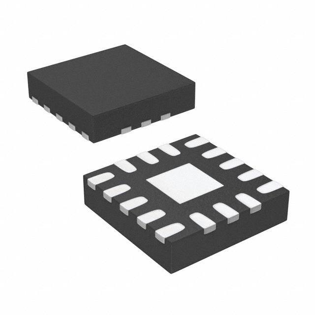
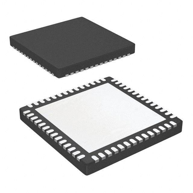
| 描述 | IC QUADRATURE MODULATOR 16-VQFN调节器/解调器 0.14GHz to 1.5GHz Analog Quad Mod |
| DevelopmentKit | TRF3701EVM |
| 产品分类 | |
| LO频率 | 140MHz ~ 1.5GHz |
| 品牌 | Texas Instruments |
| 产品手册 | |
| 产品图片 |
|
| rohs | 符合RoHS无铅 / 符合限制有害物质指令(RoHS)规范要求 |
| 产品系列 | RF集成电路,调节器/解调器,Texas Instruments TRF3701IRHC- |
| 数据手册 | |
| P1dB | 6.5dBm |
| 产品型号 | TRF3701IRHC |
| PCN设计/规格 | |
| RF频率 | 140MHz ~ 1.5GHz |
| 产品培训模块 | http://www.digikey.cn/PTM/IndividualPTM.page?site=cn&lang=zhs&ptm=26085 |
| 产品目录页面 | |
| 产品种类 | 调节器/解调器 |
| 其它名称 | 296-17198 |
| 制造商产品页 | http://www.ti.com/general/docs/suppproductinfo.tsp?distId=10&orderablePartNumber=TRF3701IRHC |
| 功能 | 调制器 |
| 包装 | 管件 |
| 单位重量 | 41.500 mg |
| 商标 | Texas Instruments |
| 安装风格 | SMD/SMT |
| 封装 | Tube |
| 封装/外壳 | 16-VQFN 裸露焊盘 |
| 封装/箱体 | VQFN-16 |
| 工作电源电压 | 4.5 V to 5.5 V |
| 工厂包装数量 | 92 |
| 最大工作温度 | + 85 C |
| 最小工作温度 | - 40 C |
| 本底噪声 | -156dBm/Hz |
| 标准包装 | 92 |
| 测试频率 | 942.5MHz |
| 电压-电源 | 4.5 V ~ 5.5 V |
| 电流-电源 | 145mA |
| 电源电流 | 0.145 A |
| 系列 | TRF3701 |
| 调制类型 | Quadrature |
| 输出功率 | -1dBm |
| 配用 | /product-detail/zh/TRF3701EVM/TRF3701EVM-ND/1908645 |

.jpg)


- 商务部:美国ITC正式对集成电路等产品启动337调查
- 曝三星4nm工艺存在良率问题 高通将骁龙8 Gen1或转产台积电
- 太阳诱电将投资9.5亿元在常州建新厂生产MLCC 预计2023年完工
- 英特尔发布欧洲新工厂建设计划 深化IDM 2.0 战略
- 台积电先进制程称霸业界 有大客户加持明年业绩稳了
- 达到5530亿美元!SIA预计今年全球半导体销售额将创下新高
- 英特尔拟将自动驾驶子公司Mobileye上市 估值或超500亿美元
- 三星加码芯片和SET,合并消费电子和移动部门,撤换高东真等 CEO
- 三星电子宣布重大人事变动 还合并消费电子和移动部门
- 海关总署:前11个月进口集成电路产品价值2.52万亿元 增长14.8%


PDF Datasheet 数据手册内容提取
TRF3701 www.ti.com SLWS145B–FEBRUARY2003–REVISEDJUNE2004 0.4 GHz to 1.5 GHz QUADRATURE MODULATOR FEATURES RHC PACKAGE • P1dBof7dBm (TOP VIEW) •• ––115560ddBBmm//HHzzNNooiisseeFatloPoOrUT=0dBm GND QREF REFVIN QVIN • TypicalUnadjustedCarrierSuppression II >35dBcat1GHz 1 16 15 14 13 • TypicalUnadjustedSidebandSuppression GND 2 12 GND >40dBcat1GHz GND 3 11 GND • DifferentialorSingle-EndedI,QInputs LO 4 10 VCC • ConvenientSingle-EndedLOInput 5 6 7 8 9 • SiliconGermaniumTechnology D C DT D N C WU N APPLICATIONS G V PO G F • CellularBaseTransceiverStationTransmit R Channel • IFSamplingApplications • TDMA:GSM,IS-136,EDGE/UWC-136 • CDMA:IS-95,UMTS,CDMA2000 • WirelessLocalLoop • WirelessLANIEEE802.11 • LMDS,MMDS • WidebandBasebandTransceivers DESCRIPTION The TRF3701 is an ultralow-noise direct quadrature modulator that is capable of converting complex input signals from baseband or IF directly up to RF. An internal analog combiner sums the real and imaginary componentsoftheRFoutputs.Thiscombinedoutput can feed the RF preamp directly at frequencies of up to 1.5 GHz. The modulator is implemented as a double-balanced mixer. An internal local oscillator (LO) phase splitter accommodatesasingle-endedLOinput,eliminatingtheneedforacostlyexternalbalun. AVAILABLEOPTIONS T 4-mm· 4-mm16-PinRHC(QFN)Package A TRF3701IRHC –40(cid:176)C to85(cid:176)C TRF3701IRHCR(TapeandReel) Pleasebeawarethatanimportantnoticeconcerningavailability,standardwarranty,anduseincriticalapplicationsofTexas Instrumentssemiconductorproductsanddisclaimerstheretoappearsattheendofthisdatasheet. PRODUCTIONDATAinformationiscurrentasofpublicationdate. Copyright©2003–2004,TexasInstrumentsIncorporated Products conform to specifications per the terms of the Texas Instruments standard warranty. Production processing does not necessarilyincludetestingofallparameters.
TRF3701 www.ti.com SLWS145B–FEBRUARY2003–REVISEDJUNE2004 FUNCTIONALBLOCKDIAGRAM VCC IVIN IREF +45° S LO RFOUT –45° 50 W QVIN QREF PWD GND TERMINALFUNCTIONS TERMINAL I/O DESCRIPTION NAME NO. GND 1,2,3,5,9,11,12 Ground IREF 15 I In-phase(I)referencevoltage/differentialinput IVIN 14 I In-phase(I)signalinput LO 4 I Localoscillatorinput PWD 7 I Powerdown QREF 16 I Quadrature(Q)referencevoltage/differentialinput QVIN 13 I Quadrature(Q)signalinput RFOUT 8 O RFoutput VCC 6,10 Supplyvoltage ABSOLUTE MAXIMUM RATINGS overoperatingfree-airtemperaturerange(unlessotherwisenoted)(1)(2) V Supplyvoltagerange –0.5Vto6V CC LOinputpowerlevel 10dBm Basebandinputvoltagelevel(single-ended) 3Vp-p T Operatingfree-airtemperaturerange –40(cid:176)C to85(cid:176)C A Leadtemperaturefor10seconds 260(cid:176)C (1) Stressesbeyondthoselistedunder"absolutemaximumratings"maycausepermanentdamagetothedevice.Thesearestressratings only,andfunctionaloperationofthedeviceattheseoranyotherconditionsbeyondthoseindicatedunder"recommendedoperating conditions"isnotimplied.Exposuretoabsolute-maximum-ratedconditionsforextendedperiodsmayaffectdevicereliability. (2) Measuredwithrespecttoground 2
TRF3701 www.ti.com SLWS145B–FEBRUARY2003–REVISEDJUNE2004 RECOMMENDED OPERATING CONDITIONS MIN NOM MAX UNIT SuppliesandReferences V Analogsupplyvoltage 4.5 5 5.5 V CC VCM(IVIN,QVIN,IREF,QREFinputcommon-modedcvoltage) 3.7 V LocalOscillatorInput(LO) Inputfrequency 400 1500 MHz Powerlevel(measuredinto50W) –6 0 6 dBm SignalInputs(IVIN,QVIN) Inputbandwidth 700 MHz ELECTRICAL CHARACTERISTICS Overrecommendedoperatingconditions,VCC=5V,VCM=3.7V,f =942.5MHzat0dBm,T =25(cid:176)C (unlessotherwise LO A noted) PARAMETER TESTCONDITIONS MIN TYP MAX UNIT PowerSupply V(PWD)=5V 145 I Totalsupplycurrent mA CC V(PWD)=0V 13 Power-downinputimpedance 11 kW Turnontime 120 ns Turnofftime 20 ns LocalOscillator(LO)Input Inputimpedance 40+j4.8 W SignalInputs(IVIN,QVIN,IREF,QREF) Inputbiascurrent V(IVIN)=V(IREF)=V(QVIN)=V(QREF)=VCM=3.7V 16 µA Single-endedinput 250 Inputimpedance kW Differentialinput 125 3
TRF3701 www.ti.com SLWS145B–FEBRUARY2003–REVISEDJUNE2004 RF OUTPUT PERFORMANCE Overrecommendedoperatingconditions,VCC=5V,VCM=3.7V,f =942.5MHzat0dBm,T =25(cid:176)C (unlessotherwise LO A noted)(1) PARAMETER TESTCONDITIONS MIN TYP MAX UNIT SingleandTwo-ToneSpecifications Outputpower –3.5 –1 dBm Secondbasebandhar- –50 –45 dBc monic(USBorLSB)(3) I,Q(2)=1Vp-p,f =928kHz BB Thirdbasebandharmonic –61 –55 dBc (USBorLSB)(3) I,Q(2)=1Vp-p(two-tonesignal,f =928kHz, IMD BB1 –55 –45 dBc 3 f =992kHz) BB2 P1dB(outputcompression 6.5 dBm point) I,Q(4)=VCM=3.7VDC –156 6-MHzoffsetfromcarrier,P =–10dBm,overtemperature –153 –151(5) out NSD Noisespectraldensity dBm/Hz 6-MHzoffsetfromcarrier,P =–5dBm,overtemperature –152 –150(5) out 6-MHzoffsetfromcarrier,P =0dBm,overtemperature –150 –148(5) out RFOUTpinimpedance 26+j3 W I,Q(2)=1Vp-p,f =928kHz,unadjusted 30 35 BB Carriersuppression I,Q(2)=1Vp-p,f =928kHz,optimized 55 dBc BB I,Q(2)=1Vp-p,f =928kHz,overtemperature 35 BB I,Q(2)=1Vp-p,f =928kHz,unadjusted 37 50 BB Sidebandsuppression I,Q(2)=1Vp-p,f =928kHz,optimized 55 dBc BB I,Q(2)=1Vp-p,f =928kHz,overtemperature 38 BB (1) Basebandinputsaredifferential;equivalentperformanceisattainedbyusingsingle-endeddrive. (2) I,Q=1Vp-pimpliesthatthemagnitudeofthesignalateachinputpinIVIN,IREF,QVIN,QREFisequalto500mVp-p. (3) USB=uppersideband.LSB=lowersideband. (4) AllinputpinstiedtoVCM (5) Maximumnoisevaluesareassuredbystatisticalcharacterizationonly,notproductiontesting.Thevaluesspecifiedareovertheentire temperaturerange,T =–40(cid:176)C to85(cid:176)C. A DEFINITIONS OF SELECTED SPECIFICATIONS Unadjusted Carrier Suppression This specification measures the amount by which the local oscillator component is attenuated in the output spectrum of the modulator relative to the carrier. It is assumed that the baseband inputs delivered to the pins of the TRF3701 are perfectly matched to have the same dc offset (VCM). This includes all four baseband inputs: IVIN,QVIN,IREFandQREF.UnadjustedcarriersuppressionismeasuredindBc. Adjusted (Optimized) Carrier Suppression This differs from the unadjusted suppression number in that the dc offsets of the baseband inputs are iteratively adjusted around their theoretical value of VCM in order to yield the maximum suppression of the LO component intheoutputspectrum.AdjustedcarriersuppressionismeasuredindBc. Unadjusted Sideband Suppression This specification measures the amount by which the unwanted sideband of the input signal is attenuated in the output of the modulator, relative to the wanted sideband. It is assumed that the baseband inputs delivered to the modulator input pins are perfectly matched in amplitude and are exactly 90(cid:176) out of phase. Unadjusted sideband suppressionismeasuredindBc. 4
TRF3701 www.ti.com SLWS145B–FEBRUARY2003–REVISEDJUNE2004 DEFINITIONS OF SELECTED SPECIFICATIONS (continued) Adjusted (Optimized) Sideband Suppression Thisdiffersfromtheunadjustedsideband suppression in that the baseband inputs are iteratively adjusted around their theoretical values to maximize the amount of sideband suppression. Adjusted sideband suppression is measuredindBc. Suppressions Over Temperature This specification assumes that the user has gone through the optimization process for the suppression in question, and set the optimal settings for the I, Q inputs at room temperature. This specification then measures thesuppressionwhentemperatureconditionschangeaftertheinitialcalibrationisdone. 5
TRF3701 www.ti.com SLWS145B–FEBRUARY2003–REVISEDJUNE2004 TYPICAL CHARACTERISTICS For all the performance plots in this section, the following conditions were used, unless otherwise noted: T = –40(cid:176)C to 85(cid:176)C, VCC = 5 V, VCM = 3.7 V, f = 942.5 MHz at P = 0 dBm, I and Q inputs driven A LO LO differentially at a frequency of 50 kHz for an output power level P = 0 dBm. In the case of optimized out suppressions, the point of optimization is noted and is always at nominal conditions and room temperature. A levelof>50dBcisassumedtobeoptimized. OUTPUTPOWER OUTPUTPOWER vs vs I,QAMPLITUDE I,QAMPLITUDE 10 10 5 5 –40°C –40°C Bm 0 85°C Bm 0 85°C − d 25°C − d 25°C er er w −5 w −5 o o P P ut ut utp −10 utp −10 O O − − UT −15 UT −15 O O P P −20 −20 fLO = 400 MHz fLO = 942.5 MHz −25 −25 0 1 2 3 4 0 1 2 3 4 I, Q Amplitude − VPP I, Q Amplitude − VPP G001 G002 Figure1. Figure2. OUTPUTPOWER SECONDUSB vs vs I,QAMPLITUDE I,QAMPLITUDE 10 0 fLO = 400 MHz −10 5 –40°C m −20 B 0 85°C d − 25°C er Bc −30 w −5 d ut Po SB − −40 utp −10 d U –40°C O n −50 − 2 UT −15 85°C O −60 P −20 −70 fLO = 1500 MHz 25°C −25 −80 0 1 2 3 4 0 1 2 3 4 I, Q Amplitude − VPP I, Q Amplitude − VPP G003 G004 Figure3. Figure4. 6
TRF3701 www.ti.com SLWS145B–FEBRUARY2003–REVISEDJUNE2004 TYPICAL CHARACTERISTICS (continued) SECONDUSB SECONDUSB vs vs I,QAMPLITUDE I,QAmplitude 0 0 fLO = 942.5 MHz fLO = 1500 MHz −10 −10 −20 −20 c −30 c B B B − d −40 –40°C B − d −30 –40°C S S U U nd2 −50 nd2 −40 85°C 25°C −60 25°C 85°C −50 −70 −80 −60 0 1 2 3 4 0 1 2 3 4 I, Q Amplitude − VPP I, Q Amplitude − VPP G005 G006 Figure5. Figure6. UNADJUSTEDCARRIERSUPPRESSION UNADJUSTEDCARRIERSUPPRESSION vs vs OUTPUTPOWER OUTPUTPOWER 50 80 c fLO = 400 MHz 85°C c fLO = 942.5 MHz dB dB 70 − − n 40 n –40°C sio sio 60 s –40°C s uppre 30 25°C uppre 50 S S arrier arrier 40 25°C C C d 20 d 30 85°C e e st st u u dj dj 20 a a n 10 n U U S − S − 10 C C 0 0 −15 −10 −5 0 5 10 −15 −10 −5 0 5 10 POUT − Output Power − dBm POUT − Output Power − dBm G007 G008 Figure7. Figure8. 7
TRF3701 www.ti.com SLWS145B–FEBRUARY2003–REVISEDJUNE2004 TYPICAL CHARACTERISTICS (continued) UNADJUSTEDCARRIERSUPPRESSION UNADJUSTEDSIDEBANDSUPPRESSION vs vs OUTPUTPOWER OUTPUTPOWER 80 60 arrier Suppression − dBc 45670000 fLO = 1–54000° MCHz eband Suppression − dBc 345000 fLO = 400 MHz –40°C d C 30 Sid 25°C 85°C ste ed 20 dju 20 25°C ust S − Una 10 85°C − Unadj 10 C S S 0 0 −15 −10 −5 0 5 10 −30 −20 −10 0 10 POUT − Output Power − dBm POUT − Output Power − dBm G009 G010 Figure9. Figure10. UNADJUSTEDSIDEBANDSUPPRESSION UNADJUSTEDSIDEBANDSUPPRESSION vs vs OUTPUTPOWER OUTPUTPOWER 60 60 85°C Bc Bc fLO = 1500 MHz d d − 50 − 50 n n o o ssi ssi –40°C e e ppr 40 25°C –40°C ppr 40 u u S S d d n n a 30 a 30 b b e e Sid Sid 25°C 85°C ed 20 ed 20 st st u u dj dj a a n 10 n 10 U U − − S fLO = 942.5 MHz S S S 0 0 −25 −15 −5 5 −30 −20 −10 0 10 POUT − Output Power − dBm POUT − Output Power − dBm G011 G012 Figure11. Figure12. 8
TRF3701 www.ti.com SLWS145B–FEBRUARY2003–REVISEDJUNE2004 TYPICAL CHARACTERISTICS (continued) THIRDLSB THIRDLSB vs vs OUTPUTPOWER OUTPUTPOWER 0 0 fLO = 400 MHz fLO = 942.5 MHz −20 −20 –40°C –40°C Bc −40 Bc −40 d d − − B B LS LS 85°C d −60 85°C d −60 r3 r3 −80 −80 25°C 25°C −100 −100 −30 −20 −10 0 10 −30 −20 −10 0 10 POUT − Output Power − dBm POUT − Output Power − dBm G013 G014 Figure13. Figure14. THIRDLSB IMD3 vs vs OUTPUTPOWER OUTPUTPOWERPERTONE 0 0 fLO = 1500 MHz fLO = 400 MHz −10 −20 −20 Bc −40 c −30 d B − d B − −40 LS 85°C D3 d −60 M r3 –40°C I −50 85°C –40°C −60 −80 −70 25°C 25°C −100 −80 −30 −20 −10 0 10 −15 −10 −5 0 POUT − Output Power − dBm POUT − Output Power Per Tone − dBm G015 G016 Figure15. Figure16. 9
TRF3701 www.ti.com SLWS145B–FEBRUARY2003–REVISEDJUNE2004 TYPICAL CHARACTERISTICS (continued) IMD3 IMD3 vs vs OUTPUTPOWERPERTONE OUTPUTPOWERPERTONE 0 0 fLO = 942.5 MHz fLO = 1500 MHz −10 −10 −20 −20 −30 Bc −30 Bc d d 3 − 25°C 3 − −40 85°C D −40 D M M I 85°C I −50 –40°C −50 −60 –40°C −60 −70 25°C −70 −80 −15 −10 −5 0 −15 −10 −5 0 POUT − Output Power Per Tone − dBm POUT − Output Power Per Tone − dBm G017 G018 Figure17. Figure18. P1dB UNADJUSTEDCARRIERSUPPRESSION vs vs FREQUENCY FREQUENCY 8 60 25°C c 85°C 7 B d − 50 n 6 85°C sio s 5 –40°C pre 40 m up B S 1dB − d 4 Carrier 30 25°C P 3 d e ust 20 –40°C 2 dj a n U 10 1 − S C 0 0 0 500 1000 1500 2000 0 500 1000 1500 2000 fLO − Frequency − MHz fLO − Frequency − MHz G019 G020 Figure19. Figure20. 10
TRF3701 www.ti.com SLWS145B–FEBRUARY2003–REVISEDJUNE2004 TYPICAL CHARACTERISTICS (continued) UNADJUSTEDSIDEBANDSUPPRESSION OUTPUTPOWERFLATNESS vs vs FREQUENCY FREQUENCY(P =0,–10dBmNOMINAL) OUT 60 2 25°C Bc 85°C d n − 50 Bm 0 o d pressi 40 ess − −2 85°C –40°C p n u at and S 30 25°C wer Fl −4 Sideb –40°C ut Po −6 ed 20 utp st O −8 Unadju 10 P − OUT −10 25°C 85°C − SS –40°C 0 −12 0 500 1000 1500 2000 850 900 950 1000 1050 fLO − Frequency − MHz fLO − Frequency − MHz G021 G022 Figure21. Figure22. SECONDUSB THIRDLSB vs vs FREQUENCY FREQUENCY −40 −40 POUT = 0 dBm POUT = 0 dBm −45 −45 −50 85°C Bc –40°C Bc −55 d d − − B −50 B −60 S S U L d d n2 r3 −65 25°C 25°C –40°C −55 −70 85°C −75 −60 −80 850 900 950 1000 1050 850 900 950 1000 1050 fLO − Frequency − MHz fLO − Frequency − MHz G023 G024 Figure23. Figure24. 11
TRF3701 www.ti.com SLWS145B–FEBRUARY2003–REVISEDJUNE2004 TYPICAL CHARACTERISTICS (continued) CARRIERSUPPRESSION SIDEBANDSUPPRESSION vs vs FREQUENCY FREQUENCY 80 80 25°C 85°C c 85°C n − dBc 60 –40°C on − dB 60 25°C sio ssi s e pre ppr –40°C p 40 u 40 u S Carrier S OptiPmoiiznattion deband OptiPmoiiznattion CS − 20 S − Si 20 S POUT = 0 dBm POUT = 0 dBm Optimized at 942.5 MHz Optimized at 942.5 MHz 0 0 850 900 950 1000 1050 850 900 950 1000 1050 fLO − Frequency − MHz fLO − Frequency − MHz G025 G026 Figure25. Figure26. OUTPUTPOWERFLATNESS CARRIERSUPPRESSION vs vs VCM(P =0dBmNOMINAL) VCM OUT 4 70 85°C fLO = 942.5 MHz 60 m B c d B − 2 d ess –40°C 25°C n − 50 25°C n o –40°C at si Fl es 40 wer 0 ppr Optimization utput Po 85°C arrier Su 30 Point O C 20 − T −2 S − U C O P 10 POUT = 0 dBm fLO = 942.5 MHz Optimized at 3.7 V −4 0 3.0 3.5 4.0 4.5 5.0 3.0 3.5 4.0 4.5 VCM − V VCM − V G027 G028 Figure27. Figure28. 12
TRF3701 www.ti.com SLWS145B–FEBRUARY2003–REVISEDJUNE2004 TYPICAL CHARACTERISTICS (continued) SIDEBANDSUPPRESSION SECONDUSB vs vs VCM VCM 70 −30 25°C 60 c −40 –40°C B –40°C n − d 50 25°C o −50 ppressi 40 85°C − dBc Su Optimization SB −60 85°C d 30 Point U an nd b 2 e −70 d Si 20 − S S 10 POUT = 0 dBm −80 fLO = 942.5 MHz POUT = 0 dBm Optimized at 3.7 V fLO = 942.5 MHz 0 −90 3.0 3.5 4.0 4.5 3.0 3.5 4.0 4.5 VCM − V VCM − V G029 G030 Figure29. Figure30. THIRDLSB SUPPLYCURRENT vs vs VCM SUPPLYVOLTAGE 0 200 POUT = 0 dBm fLO = 942.5 MHz fLO = 942.5 MHz −10 180 A −20 m − dBc −30 –40°C urrent − 160 25°C 85°C B C S y L −40 pl d p 140 r3 Su −50 85°C − C –40°C C I 120 −60 25°C −70 100 3.0 3.5 4.0 4.5 4.0 4.5 5.0 5.5 6.0 VCM − V VCC − Supply Voltage − V G031 G032 Figure31. Figure32. 13
TRF3701 www.ti.com SLWS145B–FEBRUARY2003–REVISEDJUNE2004 TYPICAL CHARACTERISTICS (continued) OUTPUTPOWERFLATNESS CARRIERSUPPRESSION vs vs SUPPLYVOLTAGE(P =0dBmNOMINAL) SUPPLYVOLTAGE OUT 3 80 fLO = 942.5 MHz 85°C 70 2 c B m d 60 B − wer − d 1 –40°C 25°C ession 50 25°C ut Po 0 uppr 40 –40°C − Outp −1 85°C arrier S 30 OptiPmoiiznattion T C POU S − 20 C −2 10 POUT = 0 dBm fLO = 942.5 MHz Optimized at 5 V −3 0 4.0 4.5 5.0 5.5 6.0 4.0 4.5 5.0 5.5 6.0 VCC − Supply Voltage − V VCC − Supply Voltage − V G033 G034 Figure33. Figure34. SIDEBANDSUPPRESSION SECONDUSB vs vs SUPPLYVOLTAGE SUPPLYVOLTAGE 80 0 POUT = 0 dBm 70 fLO = 942.5 MHz Bc 25°C 85°C −10 − d 60 n o −20 essi 50 Bc ppr –40°C − d u 40 B −30 S S band 30 OptiPmoiiznattion nd2 U e −40 d Si 25°C − 20 S S 10 POUT = 0 dBm −50 fLO = 942.5 MHz Optimized at 5 V 85°C –40°C 0 −60 4.0 4.5 5.0 5.5 6.0 4.0 4.5 5.0 5.5 6.0 VCC − Supply Voltage − V VCC − Supply Voltage − V G035 G036 Figure35. Figure36. 14
TRF3701 www.ti.com SLWS145B–FEBRUARY2003–REVISEDJUNE2004 TYPICAL CHARACTERISTICS (continued) THIRDLSB OUTPUTPOWERFLATNESS vs vs SUPPLYVOLTAGE LOINPUTPOWER(P =0dBmNOMINAL) OUT 0 3 POUT = 0 dBm fLO = 942.5 MHz −10 fLO = 942.5 MHz m 2 B d −20 − s es 1 25°C Bc −30 atn –40°C d Fl B − −40 wer 0 rd3 LS −50 85°C utput Po −1 85°C O −60 − T U O −2 −70 –40°C P 25°C −80 −3 4.0 4.5 5.0 5.5 6.0 −15 −10 −5 0 5 10 15 VCC − Supply Voltage − V PLO − Local Oscillator Input Power − dBm G037 G038 Figure37. Figure38. CARRIERSUPPRESSION vs LOCALOSCILLATORINPUTPOWER 80 70 85°C c 25°C B d 60 − n o si 50 s pre –40°C p 40 u S Optimization arrier 30 Point C − 20 S C 10 POUT = 0 dBm fLO = 942.5 MHz Optimized at 0 dBm 0 −15 −10 −5 0 5 10 15 PLO − Local Oscillator Input Power − dBm G039 Figure39. 15
TRF3701 www.ti.com SLWS145B–FEBRUARY2003–REVISEDJUNE2004 Table1.RFOUTandLOPinImpedance Frequency(MHz) Z(RFOUTPin) Z(LOPin) 100 8.59–j130.2 33.95–j106.93 200 7.12–j61.22 29.54–j52.57 300 8.52–j36.37 28.65-j31.83 400 10.5–j23.72 29.371–j19.33 500 12.82–j15.51 30.78–j11.42 600 15.26–j9.33 32.64–j6.06 700 187.1–j4.77 34.99–j1.65 800 20.8–j1.2 36.55+j1.65 900 24.2+j2.0 38.52+j3.98 1000 28.7+j4.9 40.29+j5.92 1100 32.35+j6.61 42.21+j6.98 1200 37.15+j6.88 44.09+j7.55 1300 40.55+j6.64 45.7+j7.96 1400 43.76+j6.4 47+j7.76 1500 46.6+j6.03 48.28+j7.39 SIDEBANDSUPPRESSION SECONDUSB vs vs LOCALOSCILLATORINPUTPOWER LOCALOSCILLATORINPUTPOWER 70 −35 POUT = 0 dBm 60 fLO = 942.5 MHz c 85°C −40 B d n − 50 o −45 uppressi 40 Optimization 25–°4C0°C B − dBc −50 d S 30 Point US 25°C an nd b 2 e −55 d Si 20 − –40°C S S 10 POUT = 0 dBm −60 85°C fLO = 942.5 MHz Optimized at 0 dBm 0 −65 −15 −10 −5 0 5 10 15 −15 −10 −5 0 5 10 15 PLO − Local Oscillator Input Power − dBm PLO − Local Oscillator Input Power − dBm G040 G041 Figure40. Figure41. 16
TRF3701 www.ti.com SLWS145B–FEBRUARY2003–REVISEDJUNE2004 THIRDLSB vs NOISEDISTRIBUTIONAT6MHZ LOCALOSCILLATORINPUTPOWER OFFSETOVERTEMPERATURE −40 20 POUT = 0 dBm POUT = 0 dBm 18 fLO = 942.5 MHz fLO = 942.5 MHz −50 85°C 25°C 16 14 −60 Bc e 12 B − d −70 –40°C entag 10 S c d L Per 8 r3 −80 6 4 −90 2 −100 0 6 4 2 0 8 6 4 2 0 8 6 4 −15 −10 −5 0 5 10 15 0. 0. 0. 0. 9. 9. 9. 9. 9. 8. 8. 8. 5 5 5 5 4 4 4 4 4 4 4 4 PLO − Local Oscillator Input Power − dBm −1 −1 −1 −1 −1 −1 −1 −1 −1 −1 −1 −1 G042 Noise − dBm/Hz G043 Figure42. Figure43. NOISEDISTRIBUTIONAT6MHZ NOISEDISTRIBUTIONAT6MHZ OFFSETOVERTEMPERATURE OFFSETOVERTEMPERATURE 20 20 POUT = –5 dBm POUT = –10 dBm 18 fLO = 942.5 MHz 18 fLO = 942.5 MHz 16 16 14 14 e 12 e 12 g g a a nt 10 nt 10 e e c c r r e e P 8 P 8 6 6 4 4 2 2 0 0 2 0 8 6 4 2 0 8 6 4 2 0 6 4 2 0 8 6 4 2 0 8 6 4 2 3. 3. 2. 2. 2. 2. 2. 1. 1. 1. 1. 1. 4. 4. 4. 4. 3. 3. 3. 3. 3. 2. 2. 2. 2. 5 5 5 5 5 5 5 5 5 5 5 5 5 5 5 5 5 5 5 5 5 5 5 5 5 1 1 1 1 1 1 1 1 1 1 1 1 1 1 1 1 1 1 1 1 1 1 1 1 1 − − − − − − − − − − − − − − − − − − − − − − − − − Noise − dBm/Hz Noise − dBm/Hz G044 G045 Figure44. Figure45. 17
TRF3701 www.ti.com SLWS145B–FEBRUARY2003–REVISEDJUNE2004 NOISEAT6MHzOFFSET GMSKSPECTRALPERFORMANCE vs vs OUTPUTPOWER CHANNELPOWER −135 0 fLO = 942.5 MHz Hz −10 fLO = 942.5 MHz k 0 −140 n 3 −20 c i B −30 d z − H −145 e −40 m/ 25°C nc B a d m −50 oise − −150 85°C Perfor −60 N al 400 kHz Offset ctr −70 e p −155 –40°C K S −80 S M −90 600 kHz Offset G −160 −100 −15 −10 −5 0 5 10 −12 −10 −8 −6 −4 −2 0 2 4 POUT − Output Power − dBm Channel Power − dBm G046 G047 Figure46. Figure47. GSMEDGEEVM vs CHANNELPOWER 2.5 fLO = 942.5 MHz 2.0 % − M 1.5 V E e g d M E 1.0 S G 0.5 0.0 −12 −10 −8 −6 −4 −2 0 2 4 6 Channel Power − dBm G048 Figure48. 18
TRF3701 www.ti.com SLWS145B–FEBRUARY2003–REVISEDJUNE2004 THEORY OF OPERATION The TRF3701 employs a double-balanced mixer architecture in implementing the direct I, Q upconversion. The I, Q inputs can be driven single-endedly or differentially, with comparable performance in both cases. The common mode level (VCM) of the four inputs (IVIN, IREF, QVIN, QREF) is typically set to 3.7 V and needs to be driven externally. These inputs go through a set of differential amplifiers and through a V-I converter feed the double-balanced mixers. The AC-coupled LO input to the device goes through a phase splitter to provide the in-phase and quadrature signals that in turn drive the mixers. The outputs of the mixers are then summed, converted to single-ended signals, and amplified before they are fed to the output port RFOUT. The output of the TRF3701isac-coupledandcandrive50-W loads. EQUIVALENT CIRCUITS Figure49throughFigure52showequivalentschematicsforthemaininputsandoutputsofthedevice. LO 50 W IQ Baseband S0001-01 S0002-01 Figure49.LOEquivalentInputCircuit Figure50.IVIN,QVIN,IREF,QREFEquivalentCircuit 50 kW Power Down RFOUT S0004-01 S0003-01 Figure51.RFOUTEquivalentCircuit Figure52.Power-Down(PWD)EquivalentCircuit 19
TRF3701 www.ti.com SLWS145B–FEBRUARY2003–REVISEDJUNE2004 APPLICATION INFORMATION DRIVING THE I, Q INPUTS There are several ways to drive the four baseband inputs of the TRF3701 to the required amplitude and dc offset. The optimal configuration depends on the end application requirements and the signal levels desired by thedesigner. The TRF3701 is by design a differential part, meaning that ideally the user should provide fully complementary signals.However,similar performance in every respect can be achieved if the user only has single-ended signals available.Inthiscase,theIREFandQREFpinsjustneedtohavetheVCMdcoffsetapplied. ImplementingaSingle-to-DifferentialConversionfortheI,Qinputs IncasedifferentialI,Qsignalsaredesiredbutnotavailable,theTHS4503familyofwideband,low-distortion,fully differential amplifiers can be used to provide a convenient way of performing this conversion. Even if differential signalsareavailable,theTHS4503canprovidegainincaseahighervoltageswingisrequired.Besidesfeaturing high bandwidth and high linearity, the THS4503 also provides a convenient way of applying the VCM to all four inputs to the modulator through the VOCM pin (pin 2). The user can further adjust the dc levels for optimum carrier suppression by injecting extra dc at the inputs to the operational amplifier, or by individually adding it to the four outputs. Figure 53 shows a typical implementation of the THS4503 as a driver for the TRF3701. Gain canbeeasilyincorporatedintheloop by adjusting the feedback resistors appropriately. For more details, see the THS4503datasheetatwww.ti.com. 20
TRF3701 www.ti.com SLWS145B–FEBRUARY2003–REVISEDJUNE2004 APPLICATION INFORMATION (continued) 10 pF 392 W +8 VA VCM 0.01 m F 0.1 m F 0.01 m F 0.1 m F 7 3 THS4503 NC +VCC 374 W 5 22.1 W IREF 8 IREF Single-Ended I Input + VOUT− 2 VOCM 402 W 1 VOUT+ 4 22.1 W IVIN − IVIN −VCC 6 −8 VA 0.1 m F 0.01 m F 392 W 10 pF S0005-02 Figure53.UsingtheTHS4503toConditiontheBasebandInputstotheTRF3701(IChannelShown) DRIVING THE LOCAL OSCILLATOR INPUT The LO pin is internally terminated to 50 W, thus enabling easy interface to the LO source without the need for external impedance matching. The power level of the LO signal should be in the range of –6 to 6 dBm. For characterization purposes, a power level of 0 dBm was chosen. An ideal way of driving the LO input of the TRF3701 is by using the TRF3750, an ultralow-phase-noise integer-N PLL from Texas Instruments. Combining the TRF3750 with an external VCO can complete the loop and provide a flexible, convenient and cost-effective 21
TRF3701 www.ti.com SLWS145B–FEBRUARY2003–REVISEDJUNE2004 APPLICATION INFORMATION (continued) solution for the local oscillator of the transmitter. Figure 54 shows a typical application for the LO driver network that incorporates the TRF3750 integer-N PLL synthesizer into the design. Depending on the VCO output and the amount of signal loss, an optional gain stage may be added to the output of the VCO before it is applied to the TRF3701LOinput. DVDD VCP + 10 pF AVDD VVCO To TRF3701 10 (cid:2)F 0.1 (cid:2)F 0.1 (cid:2)F + LO Input + 10 pF 10 pF 10 (cid:2)F 10 pF + 10 (cid:2)F 10 (cid:2)F 0.1 (cid:2)F 0.1 (cid:2)F 100 pF 5 7 1 SUPPLY 10 CE AVDD DVDD VCP 16 16.5 (cid:1) 1 nF TCXO 8 2 20 k(cid:1) V TUNE OUT 16.5 (cid:1) REFIN CPOUT (10-MHz GND Reference) TRF3750 1 nF 10 nF 82 pF VCO 100 pF GND GND 16.5 (cid:1) RSET 1 RSET 3.9 k(cid:1) DECOUPLING NOT SHOWN 4.7 k(cid:1) CLK 11 CLK RFINA 6 DATA 12 DATA MUXOUT 14 LOCK DETECT 100 pF 49.9 (cid:1) D N D D LE 13 LE PG GN GNRFINB 5 C A D 3 4 9 100 pF Figure54.TypicalApplicationCircuitforGeneratingtheLOSignalfortheTRF3701Modulator PCB LAYOUT CONSIDERATIONS The TRF3701 is a high-performance RF device; hence, care should be taken in the layout of the PCB in order to ensure optimum performance. Proper decoupling with low ESR capacitors is needed for the VCC supplies (pins 6 and 10). Typical values used are in the order of 1 pF in parallel to 0.1 µF, with the lower-valued capacitors placedclosertothedevicepins.Inaddition,a larger tank capacitor in the order of 10 µF should be placed on the supply line as layout permits. At least a 4-layer board is recommended for the PCB. If possible, a solid ground plane and a ground pour is also recommended, as is a power plane for the supplies. Because the balance of the four I, Q inputs to the modulator can be critical to device performance, care should be taken to ensure that the trace runs for all four inputs are equidistant. In the case of single-ended drive of the I, Q inputs, the two unused pins IREF and QREF are fed with the VCM dc voltage only, and should be decoupled with a 0.1-mF capacitor (or smaller). The LO input trace should be minimized in length and have controlled impedance of 50 W. No external matching components are needed because there is an internal 50-W termination. The RFOUT pin should also have a relatively small trace to minimize parasitics and coupling, and should also be controlled to 50 W. An impedance-matching network can be used to optimize power transfer, but is not critical. All the results shown in the data sheet were taken with no impedance matching network used (RFOUT directly driving an external 50-W load). The exposed thermal and ground pad on the bottom of the TRF3701 should be soldered to ground to ensure optimum electrical and thermal performance. The landing pattern on the PCB should include a solid pad and 4 thermal vias. These vias typically have 1,2-mm pitch and 0,3-mm diameter. The vias can be arranged in a 2·2 array.ThethermalpadonthePCBshouldbeatleast1.65·1.65 mm. IMPLEMENTING A DIRECT UPCONVERSION TRANSMITTER USING A TI CommsDAC The TRF3701 is ideal for implementing a direct upconversion transmitter, where the input I, Q data can originate from an ASIC or a DAC. Texas Instruments' line of digital-to-analog converters (DAC) is ideally suited for interfacingtotheTRF3701.SuchDACsinclude,amongothers,theDAC290xseries,DAC5672,andDAC5686. 22
TRF3701 www.ti.com SLWS145B–FEBRUARY2003–REVISEDJUNE2004 APPLICATION INFORMATION (continued) This section illustrates the use of the DAC5686, which offers a unique set of features that make interfacing to the TRF3701 easy and convenient. The DAC5686 is a 16-bit, 500 MSPS, 2·–16· interpolating dual-channel DAC, and it features I, Q adjustments for optimal interface to the TRF3701. User-selectable, 11-bit offset and 12-bit gain adjustments can optimize the carrier and sideband suppression of the modulator, resulting in enhanced performanceandrelaxedfilteringrequirementsatRF.Thepreferred mode of operation of the DAC5686 for direct interface with the TRF3701 at baseband is the dual-DAC mode. The user also has the flexibility of selecting any one of the four possible complex spectral bands to be fed into the TRF3701. For details on the available modes andprogramming,seetheDAC5686datasheetavailableatwww.ti.com. Figure 55 shows the DAC5686 in dual-DAC mode, which is best-suited for zero-IF interface to the TRF3701. In this mode, a seamless, passive interface between the DAC output and the input to the modulator is used, so that no extra components are needed between the two devices. The optimum dc offset level for the inputs to the TRF3701 (VCM) is approximately 3.7 V. The output of the DAC should be centered around 3.3 V or less (depending on signal swing), in order to ensure that its output compliance limits are not exceeded. The resistive network shown in Figure 55 allows for this dc offset transition while still providing a dc path between the DAC output and the modulator. This ensures that the dc offset adjustments on the DAC5686 can still be applied to optimize the carrier suppression at the modulator output. The combination of the DAC5686 and the TRF3701 providesauniquesignal-chainsolutionwithstate-of-the-artperformanceforwirelessinfrastructureapplications. +3.3 V +5 V VCC A IOUTA1 IVIN Fdata Offset IREF DEMUX 16-Bit DAC IOUTA2 DA[15:0] A Gain +45° S LO RFOUT –45° B Gain 50 W 16-Bit DB[15:0] IOUTB1 DAC QVIN B Offset IOUTB2 QREF DAC5686 TRF3701 PWD GND +3.3 V +5 V Figure55.DAC5686inDual-DACModewithQuadratureModulator 23
MECHANICAL DATA MPQF132 – JUNE 2002 RHC (S–PQFP–N16) (CUSTOM PACKAGE) PLASTIC QUAD FLATPACK 4,15 A 3,85 B ÏÏÏÏ 4,15 3,85 ÏÏÏÏ 16 ÏÏÏÏ 1 ÏÏÏÏ PIN 1 INDEX AREA 2 TOP AND BOTTOM 1,00 0,20 NOMINAL 0,80 LEAD FRAME 0,08 C SEATING PLANE 0,05 C 0,00 1,65 MAX 0,725 0,80 16(cid:1) PIN 1 CHAMBER 0,525 2 1 5 16 1,65 MAX 9 EXPOSED THERMAL DIE PAD 12 D 16(cid:1)0,435 0,10 0,315 BOTTOM VIEW 4204353/A 05/02 NOTES: A. All linear dimensions are in millimeters. B. This drawing is subject to change without notice. C. QFN (Quad Flatpack No–Lead) Package configuration. D. The Package thermal performance may be enhanced by bonding the thermal die pad to an external thermal plane. This pad is electrically and thermally connected to the backside of the die and possibly selected ground leads. POST OFFICE BOX 655303 • DALLAS, TEXAS 75265 1
None
IMPORTANT NOTICE Texas Instruments Incorporated and its subsidiaries (TI) reserve the right to make corrections, modifications, enhancements, improvements, and other changes to its products and services at any time and to discontinue any product or service without notice. Customers should obtain the latest relevant information before placing orders and should verify that such information is current and complete. All products are sold subject to TI’s terms and conditions of sale supplied at the time of order acknowledgment. TI warrants performance of its hardware products to the specifications applicable at the time of sale in accordance with TI’s standard warranty. Testing and other quality control techniques are used to the extent TI deems necessary to support this warranty. Except where mandated by government requirements, testing of all parameters of each product is not necessarily performed. TI assumes no liability for applications assistance or customer product design. Customers are responsible for their products and applications using TI components. To minimize the risks associated with customer products and applications, customers should provide adequate design and operating safeguards. TI does not warrant or represent that any license, either express or implied, is granted under any TI patent right, copyright, mask work right, or other TI intellectual property right relating to any combination, machine, or process in which TI products or services are used. Information published by TI regarding third-party products or services does not constitute a license from TI to use such products or services or a warranty or endorsement thereof. Use of such information may require a license from a third party under the patents or other intellectual property of the third party, or a license from TI under the patents or other intellectual property of TI. Reproduction of information in TI data books or data sheets is permissible only if reproduction is without alteration and is accompanied by all associated warranties, conditions, limitations, and notices. Reproduction of this information with alteration is an unfair and deceptive business practice. TI is not responsible or liable for such altered documentation. Resale of TI products or services with statements different from or beyond the parameters stated by TI for that product or service voids all express and any implied warranties for the associated TI product or service and is an unfair and deceptive business practice. TI is not responsible or liable for any such statements. Following are URLs where you can obtain information on other Texas Instruments products and application solutions: Products Applications Amplifiers amplifier.ti.com Audio www.ti.com/audio Data Converters dataconverter.ti.com Automotive www.ti.com/automotive DSP dsp.ti.com Broadband www.ti.com/broadband Interface interface.ti.com Digital Control www.ti.com/digitalcontrol Logic logic.ti.com Military www.ti.com/military Power Mgmt power.ti.com Optical Networking www.ti.com/opticalnetwork Microcontrollers microcontroller.ti.com Security www.ti.com/security Telephony www.ti.com/telephony Video & Imaging www.ti.com/video Wireless www.ti.com/wireless Mailing Address: Texas Instruments Post Office Box 655303 Dallas, Texas 75265 Copyright 2004, Texas Instruments Incorporated