ICGOO在线商城 > 射频/IF 和 RFID > RF 调制器 > ADRF6701ACPZ-R7
 Datasheet下载
- 型号: ADRF6701ACPZ-R7
- 制造商: Analog
- 库位|库存: xxxx|xxxx
- 要求:
| 数量阶梯 | 香港交货 | 国内含税 |
| +xxxx | $xxxx | ¥xxxx |
查看当月历史价格
查看今年历史价格
ADRF6701ACPZ-R7产品简介:
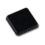
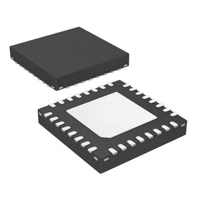
ICGOO电子元器件商城为您提供ADRF6701ACPZ-R7由Analog设计生产,在icgoo商城现货销售,并且可以通过原厂、代理商等渠道进行代购。 ADRF6701ACPZ-R7价格参考。AnalogADRF6701ACPZ-R7封装/规格:RF 调制器, RF Modulator IC 400MHz ~ 1.25GHz 40-VFQFN Exposed Pad, CSP。您可以下载ADRF6701ACPZ-R7参考资料、Datasheet数据手册功能说明书,资料中有ADRF6701ACPZ-R7 详细功能的应用电路图电压和使用方法及教程。
ADRF6701ACPZ-R7 是由 Analog Devices Inc.(ADI)公司生产的一款射频(RF)调制器芯片,属于直接变频调制器类别。该器件广泛应用于需要高性能射频信号生成的通信系统中。

其主要应用场景包括:

1. 无线通信基站:ADRF6701 适用于蜂窝通信系统中的发射模块,如4G LTE和5G通信基站,能够实现基带信号到射频信号的高效调制。

2. 微波回传系统:在点对点微波通信中,该芯片可用于实现高线性度、低失真的射频信号调制,保障数据传输质量。

3. 测试与测量设备:作为信号发生模块的一部分,ADRF6701 可用于射频测试仪器中,生成高精度调制信号,用于设备性能评估。

4. 工业与医疗通信系统:在需要高稳定性和高集成度的专用通信系统中,如工业自动化无线接口或远程医疗设备,该芯片也具有广泛应用。

5. 软件定义无线电(SDR)平台:由于其支持宽频带和灵活频率配置,适合用于软件无线电系统中,实现多模式通信。

该芯片集成了本振(LO)合成器、混频器和滤波器等功能模块,支持IQ调制,具备良好的线性度和调制精度,适合高性能射频发射需求。
| 参数 | 数值 |
| 产品目录 | |
| 描述 | IC MOD QUAD FRAC N PLL 40LFCSP调节器/解调器 400-1250MHz Quadrature |
| 产品分类 | |
| LO频率 | 750MHz ~ 1.15GHz |
| 品牌 | Analog Devices |
| 产品手册 | |
| 产品图片 |
|
| rohs | 符合RoHS无铅 / 符合限制有害物质指令(RoHS)规范要求 |
| 产品系列 | RF集成电路,调节器/解调器,Analog Devices ADRF6701ACPZ-R7- |
| 数据手册 | |
| P1dB | 10.3dB |
| 产品型号 | ADRF6701ACPZ-R7 |
| RF频率 | 400MHz ~ 1.25GHz |
| 产品种类 | 调节器/解调器 |
| 其它名称 | ADRF6701ACPZ-R7DKR |
| 功能 | 调制器 |
| 包装 | Digi-Reel® |
| 商标 | Analog Devices |
| 安装风格 | SMD/SMT |
| 封装 | Reel |
| 封装/外壳 | 40-VFQFN 裸露焊盘,CSP |
| 封装/箱体 | LFCSP-40 |
| 工作温度范围 | - 40 C to + 85 C |
| 工作电压 | 4.75 V to 5.25 V |
| 工作电流 | 240 mA |
| 工作电源电压 | 4.75 V to 5.25 V |
| 工厂包装数量 | 750 |
| 接口类型 | SPI |
| 最大工作温度 | + 85 C |
| 最小工作温度 | - 40 C |
| 本底噪声 | -159.4dBm/Hz |
| 标准包装 | 1 |
| 测试频率 | 1.1GHz |
| 电压-电源 | 4.75 V ~ 5.25 V |
| 电流-电源 | 290mA |
| 电源电流 | 240 mA |
| 类型 | Modulator |
| 系列 | ADRF6701 |
| 视频文件 | http://www.digikey.cn/classic/video.aspx?PlayerID=1364138032001&width=640&height=505&videoID=2245193150001http://www.digikey.cn/classic/video.aspx?PlayerID=1364138032001&width=640&height=505&videoID= 2474683260001 |
| 调制类型 | Quadrature |
| 输出功率 | 2.1dBm |


- 商务部:美国ITC正式对集成电路等产品启动337调查
- 曝三星4nm工艺存在良率问题 高通将骁龙8 Gen1或转产台积电
- 太阳诱电将投资9.5亿元在常州建新厂生产MLCC 预计2023年完工
- 英特尔发布欧洲新工厂建设计划 深化IDM 2.0 战略
- 台积电先进制程称霸业界 有大客户加持明年业绩稳了
- 达到5530亿美元!SIA预计今年全球半导体销售额将创下新高
- 英特尔拟将自动驾驶子公司Mobileye上市 估值或超500亿美元
- 三星加码芯片和SET,合并消费电子和移动部门,撤换高东真等 CEO
- 三星电子宣布重大人事变动 还合并消费电子和移动部门
- 海关总署:前11个月进口集成电路产品价值2.52万亿元 增长14.8%


PDF Datasheet 数据手册内容提取
400 MHz to 1250 MHz Quadrature Modulator with 750 MHz to 1150 MHz Frac-N PLL and Integrated VCO Data Sheet ADRF6701 FEATURES modulator, PLL, and VCO provides for significant board savings and reduces the BOM and design complexity. IQ modulator with integrated fractional-N PLL Output frequency range: 400 MHz to 1250 MHz The integrated fractional-N PLL/synthesizer generates a 2× f LO Internal LO frequency range: 750 MHz to 1150 MHz input to the IQ modulator. The phase detector together with an Output P1dB: 10.3 dBm @ 1100 MHz external loop filter is used to control the VCO output. The VCO Output IP3: 30.1 dBm @ 1100 MHz output is applied to a quadrature divider. To reduce spurious Noise floor: −159.4 dBm/Hz @ 1100 MHz components, a sigma-delta (Σ-Δ) modulator controls the Baseband bandwidth: 750 MHz (3 dB) programmable PLL divider. SPI serial interface for PLL programming The IQ modulator has wideband differential I and Q inputs, Integrated LDOs and LO buffer which support baseband as well as complex IF architectures. Power supply: 5 V/240 mA The single-ended modulator output is designed to drive a 50 Ω 40-lead 6 mm × 6 mm LFCSP load impedance and can be disabled. APPLICATIONS The ADRF6701 is fabricated using an advanced silicon-germanium Cellular communications systems BiCMOS process. It is available in a 40-lead, exposed-paddle, Pb- GSM/EDGE, CDMA2000, W-CDMA, TD-SCDMA, LTE free, 6 mm × 6 mm LFCSP package. Performance is specified from Broadband wireless access systems −40°C to +85°C. A lead-free evaluation board is available. Satellite modems Table 1. GENERAL DESCRIPTION IQ Modulator Part No. Internal LO Range ±3 dB RF Output Range The ADRF6701 provides a quadrature modulator and ADRF6701 750 MHz 400 MHz synthesizer solution within a small 6 mm × 6 mm footprint 1150 MHz 1250 MHz while requiring minimal external components. ADRF6702 1550 MHz 1200 MHz The ADRF6701 is designed for RF outputs from 400 MHz to 2150 MHz 2400 MHz 1250 MHz. The low phase noise VCO and high performance ADRF6703 2100 MHz 1550 MHz 2600 MHz 2650 MHz quadrature modulator make the ADRF6701 suitable for next ADRF6704 2500 MHz 2050 generation communication systems requiring high signal 290 MHz 3000 MHz dynamic range and linearity. The integration of the IQ FUNCTIONAL BLOCK DIAGRAM VCC7 VCC6 VCC5 VCC4 VCC3 VCC2 VCC1 34 29 27 22 17 10 1 LOSEL 36 ADRF6701 LON 37 40 DECL3 BUFFER DIV÷ID2ER 9 DECL2 LOP 38 BUFFER 2:1 DIVIDER 2 DECL1 DACTLAK 1132 INTESRPFIACE FRARCETGION MODULUS INTREEGGER MUX ÷2 LE 14 THIRD-ORDER INFTREARCPTOIOLANTAOLR VCO 18 QP ×2 N COUNTER PRESCALER CORE ÷2 19 QN REFIN 6 21 TO 123 ÷2 0/90 32 IN ÷2 MUX – PHASE C25H0AµRAG,E PUMP 33 IP ÷4 TEMP + FREQUENCY 500µA (DEFAULT), SENSOR DETECTOR 750µA, MUXOUT 8 1000µA 4 7 11 15 20 21 23 25 28 30 31 35 24 5 3 39 16 26 N1.O NTCE S= NO CONNECT. DO NOT CONNECTTO TGHNISD PIN. NC RSET CPVTUNE ENOP RFOUT 08567-001 Figure 1. Rev. A Information furnished by Analog Devices is believed to be accurate and reliable. However, no responsibility is assumed by Analog Devices for its use, nor for any infringements of patents or other One Technology Way, P.O. Box 9106, Norwood, MA 02062-9106, U.S.A. rights of third parties that may result from its use. Specifications subject to change without notice. No license is granted by implication or otherwise under any patent or patent rights of Analog Devices. Tel: 781.329.4700 www.analog.com Trademarks and registered trademarks are the property of their respective owners. Fax: 781.461.3113 ©2011–2012 Analog Devices, Inc. All rights reserved.
ADRF6701 Data Sheet TABLE OF CONTENTS Features .............................................................................................. 1 Device Programming and Register Sequencing ..................... 19 Applications ....................................................................................... 1 Register Summary .......................................................................... 20 General Description ......................................................................... 1 Register Description ....................................................................... 21 Functional Block Diagram .............................................................. 1 Register 0—Integer Divide Control (Default: 0x0001C0) .... 21 Revision History ............................................................................... 2 Register 1—Modulus Divide Control (Default: 0x003001) .. 22 Specifications ..................................................................................... 3 Register 2—Fractional Divide Control (Default: 0x001802) 22 Timing Characteristics ................................................................ 6 Register 3—Σ-Δ Modulator Dither Control (Default: 0x10000B) .................................................................................... 23 Absolute Maximum Ratings ............................................................ 7 ESD Caution .................................................................................. 7 Register 4—PLL Charge Pump, PFD, and Reference Path Control (Default: 0x0AA7E4) ................................................... 24 Pin Configuration and Function Descriptions ............................. 8 Register 5—LO Path and Modulator Control (Default: Typical Performance Characteristics ........................................... 10 0x0000D5) ................................................................................... 26 Theory of Operation ...................................................................... 16 Register 6—VCO Control and VCO Enable (Default: PLL + VCO .................................................................................. 16 0x1E2106) .................................................................................... 27 Basic Connections for Operation ............................................. 16 Register 7—External VCO Enable and Second lo divider .... 27 External LO ................................................................................. 16 Characterization Setups ................................................................. 28 Loop Filter ................................................................................... 17 Evaluation Board ............................................................................ 30 DAC-to-IQ Modulator Interfacing .......................................... 18 Evaluation Board Control Software ......................................... 30 Adding a Swing-Limiting Resistor ........................................... 18 Outline Dimensions ....................................................................... 35 IQ Filtering .................................................................................. 19 Ordering Guide .......................................................................... 35 Baseband Bandwidth ................................................................. 19 REVISION HISTORY 6/12—Rev. 0 to Rev. A Changes to Table 1 ............................................................................ 1 Changes to the Device Programming and Register Sequencing Section ........................................................................ 19 Changes to Figure 45 ...................................................................... 25 9/11—Revision 0: Initial Version Rev. A | Page 2 of 36
Data Sheet ADRF6701 SPECIFICATIONS V = 5 V; T = 25°C; baseband I/Q amplitude = 1 V p-p differential sine waves in quadrature with a 500 mV dc bias; baseband I/Q S A frequency (f ) = 1 MHz; f = 38.4 MHz; f = 153.6 MHz at +4 dBm Re:50 Ω (1 V p-p); 130 kHz loop filter, unless otherwise noted. BB PFD REF Table 2. Parameter Test Conditions/Comments Min Typ Max Unit OPERATING FREQUENCY RANGE IQ modulator (±3 dB RF output range) 400 1250 MHz PLL LO range 750 1150 MHz RF OUTPUT = 800 MHz RFOUT pin Nominal Output Power Baseband VIQ = 1 V p-p differential 4.4 dBm IQ Modulator Voltage Gain RF output divided by baseband input voltage 0.4 dB OP1dB 12.5 dBm Carrier Feedthrough −49.9 dBm Sideband Suppression −53.9 dBc Quadrature Error −0.75 Degrees I/Q Amplitude Balance 0.03 dB Second Harmonic P − P (f ± (2 × f )) −81.9 dBc OUT LO BB Third Harmonic P − P (f ± (3 × f )) −58.8 dBc OUT LO BB Output IP2 f1 = 3.5 MHz, f2 = 4.5 MHz, P ≈ −2 dBm per tone >70 dBm BB BB OUT Output IP3 f1 = 3.5 MHz, f2 = 4.5 MHz, P ≈ −2 dBm per tone 30.8 dBm BB BB OUT Noise Floor I/Q inputs = 0 V differential with 500 mV dc bias, 20 MHz carrier offset −157.9 dBm/Hz RF OUTPUT = 950 MHz RFOUT pin Nominal Output Power Baseband VIQ = 1 V p-p differential 3.8 dBm IQ Modulator Voltage Gain RF output divided by baseband input voltage −0.2 dB OP1dB 11.2 dBm Carrier Feedthrough −46.2 dBm Sideband Suppression −45.4 dBc Quadrature Error −0.5 Degrees I/Q Amplitude Balance 0.03 dB Second Harmonic P − P (f ± (2 × f )) −76.5 dBc OUT LO BB Third Harmonic P − P (f ± (3 × f )) −59.1 dBc OUT LO BB Output IP2 f1 = 3.5 MHz, f2 = 4.5 MHz, P ≈ −2 dBm per tone >70 dBm BB BB OUT Output IP3 f1 = 3.5 MHz, f2 = 4.5 MHz, P ≈ −2 dBm per tone 31.7 dBm BB BB OUT Noise Floor I/Q inputs = 0 V differential with 500 mV dc bias, 20 MHz carrier offset −157.9 dBm/Hz RF OUTPUT = 1100 MHz RFOUT pin Nominal Output Power Baseband VIQ = 1 V p-p differential 2.1 dBm IQ Modulator Voltage Gain RF output divided by baseband input voltage −1.9 dB OP1dB 10.3 dBm Carrier Feedthrough −49.9 dBm Sideband Suppression −47.2 dBc Quadrature Error −0.5 Degrees I/Q Amplitude Balance 0.03 dB Second Harmonic P − P (f ± (2 × f )) −77.7 dBc OUT LO BB Third Harmonic P − P (f ± (3 × f )) −60.3 dBc OUT LO BB Output IP2 f1 = 3.5 MHz, f2 = 4.5 MHz, P ≈ −2 dBm per tone >70 dBm BB BB OUT Output IP3 f1 = 3.5 MHz, f2 = 4.5 MHz, P ≈ −2 dBm per tone) 30.1 dBm BB BB OUT Noise Floor I/Q inputs = 0 V differential with 500 mV dc bias, 20 MHz carrier offset −159.4 dBm/Hz SYNTHESIZER SPECIFICATIONS Synthesizer specifications referenced to the modulator output Internal LO Range 750 1150 MHz Figure of Merit (FOM)1 −222 dBc/Hz/Hz Rev. A | Page 3 of 36
ADRF6701 Data Sheet Parameter Test Conditions/Comments Min Typ Max Unit REFERENCE CHARACTERISTICS REFIN, MUXOUT pins REFIN Input Frequency 12 160 MHz REFIN Input Capacitance 4 pF Phase Detector Frequency 20 40 MHz MUXOUT Output Level Low (lock detect output selected) 0.25 V High (lock detect output selected) 2.7 V MUXOUT Duty Cycle 50 % CHARGE PUMP Charge Pump Current Programmable to 250 µA, 500 µA, 750 µA, 1000 µA 500 µA Output Compliance Range 1 2.8 V PHASE NOISE (FREQUENCY = Closed loop operation (see Figure 35 for loop filter design) 800 MHz, f = 38.4 MHz) PFD 10 kHz offset −114 dBc/Hz 100 kHz offset −112 dBc/Hz 1 MHz offset −135 dBc/Hz 10 MHz offset −154 dBc/Hz Integrated Phase Noise 1 kHz to 10 MHz integration bandwidth 0.09 °rms Reference Spurs f /2 −113 dBc PFD f −101 dBc PFD f × 2 −99 dBc PFD f × 3 −108 dBc PFD f × 4 −99 dBc PFD PHASE NOISE (FREQUENCY = Closed loop operation (see Figure 35 for loop filter design) 950 MHz, f = 38.4 MHz) PFD 10 kHz offset −112 dBc/Hz 100 kHz offset −111 dBc/Hz 1 MHz offset −133 dBc/Hz 10 MHz offset −153 dBc/Hz Integrated Phase Noise 1 kHz to 10 MHz integration bandwidth 0.11 °rms Reference Spurs f /2 −113 dBc PFD f −106 dBc PFD f × 2 −104 dBc PFD f × 3 −100 dBc PFD f × 4 −107 dBc PFD PHASE NOISE (FREQUENCY = Closed loop operation (see Figure 35 for loop filter design) 1100 MHz, f = 38.4 MHz) PFD 10 kHz offset −113 dBc/Hz 100 kHz offset −108 dBc/Hz 1 MHz offset −135 dBc/Hz 10 MHz offset −153 dBc/Hz Integrated Phase Noise 1 kHz to 10 MHz integration bandwidth 0.12 °rms Reference Spurs f /2 −112 dBc PFD f −93 dBc PFD f × 2 −93 dBc PFD f × 3 −105 dBc PFD f × 4 −103 dBc PFD RF OUTPUT HARMONICS Measured at RFOUT, frequency = 1100 MHz Second harmonic −61 dBc Third harmonic −73 dBc Rev. A | Page 4 of 36
Data Sheet ADRF6701 Parameter Test Conditions/Comments Min Typ Max Unit LO INPUT/OUTPUT LOP, LON Output Frequency Range Divide by 4 circuit in LO path enabled 750 1150 MHz Divide by 2 circuit in LO path disabled 1500 2300 MHz Dividers in LO path disabled 3000 4600 MHz LO Output Level at 950 MHz 2× LO or 1× LO mode, into a 50 Ω load, LO buffer enabled 2.5 dBm LO Input Level Externally applied 2× LO, PLL disabled 0 dBm LO Input Impedance Externally applied 2× LO, PLL disabled 50 Ω BASEBAND INPUTS IP, IN, QP, QN pins I and Q Input DC Bias Level 400 500 600 mV Bandwidth P ≈ −7 dBm, RF flatness of IQ modulator output calibrated out OUT 0.5 dB 350 MHz 3 dB 750 MHz Differential Input Impedance 920 Ω Differential Input Capacitance 1 pF LOGIC INPUTS CLK, DATA, LE, ENOP, LOSEL Input High Voltage, V 1.4 3.3 V INH Input Low Voltage, V 0 0.7 V INL Input Current, I /I 0.1 µA INH INL Input Capacitance, C 5 pF IN TEMPERATURE SENSOR VPTAT voltage measured at MUXOUT Output Voltage T = 25°C, RL ≥10 kΩ (LO buffer disabled) 1.63 V A Temperature Coefficient T = −40°C to +85°C, RL ≥10 kΩ 3.75 mV/°C A POWER SUPPLIES VCC1, VCC2, VCC3, VCC4, VCC5, VCC6, VCC7 Voltage Range 4.75 5 5.25 V Supply Current Normal Tx mode (PLL and IQMOD enabled, LO buffer disabled) 240 mA Tx mode using external LO input (internal VCO/PLL disabled) 130 mA Tx mode with LO buffer enabled 290 mA Power-down mode 22 µA 1 The figure of merit (FOM) is computed as phase noise (dBc/Hz) – 10log10(fPFD) – 20log10(fLO/fPFD). The FOM was measured across the full LO range, with fREF = 80 MHz, fREF power = 10 dBm (500 V/μs slew rate) with a 40 MHz fPFD. The FOM was computed at 50 kHz offset. Rev. A | Page 5 of 36
ADRF6701 Data Sheet TIMING CHARACTERISTICS Table 3. Parameter Limit Unit Test Conditions/Comments t 20 ns min LE to CLK setup time 1 t 10 ns min DATA to CLK setup time 2 t 10 ns min DATA to CLK hold time 3 t 25 ns min CLK high duration 4 t 25 ns min CLK low duration 5 t 10 ns min CLK to LE setup time 6 t 20 ns min LE pulse width 7 t4 t5 CLK t2 t3 DB2 DB1 DB0 (LSB) DATA DB23 (MSB) DB22 (CONTROL BIT C3) (CONTROL BIT C2) (CONTROL BIT C1) t6 t7 t1 LE 08567-002 Figure 2. Timing Diagram Rev. A | Page 6 of 36
Data Sheet ADRF6701 ABSOLUTE MAXIMUM RATINGS Stresses above those listed under Absolute Maximum Ratings Table 4. may cause permanent damage to the device. This is a stress Parameter Rating rating only; functional operation of the device at these or any Supply Voltage (VCC1 to VCC7) 5.5 V other conditions above those indicated in the operational Digital I/O, CLK, DATA, LE −0.3 V to +3.6 V section of this specification is not implied. Exposure to absolute LOP, LON 18 dBm maximum rating conditions for extended periods may affect IP, IN, QP, QN −0.5 V to +1.5 V device reliability. REFIN −0.3 V to +3.6 V θ (Exposed Paddle Soldered Down)1 35°C/W JA Maximum Junction Temperature 150°C ESD CAUTION Operating Temperature Range −40°C to +85°C Storage Temperature Range −65°C to +150°C 1 Per JDEC standard JESD 51-2. Rev. A | Page 7 of 36
ADRF6701 Data Sheet PIN CONFIGURATION AND FUNCTION DESCRIPTIONS 3E L LCEDNUTVPOLNOLESOLDNG7CCVPINIDNG 0987654321 4333333333 VCC1 1 PIN1 30GND DECL1 2 INDICATOR 29VCC6 CP 3 28GND RGSNEDT 45 ADRF6701 2267RVCFOCU5T REFIN 6 TOPVIEW 25GND GND 7 (NottoScale) 24NC MUXOUT 8 23GND DECL2 9 22VCC4 VCC210 21GND 11213141516171819102 DAKEDP3PND NGTADLCLNGONECCVQQNG NOTES 12..NLTOHCEW=ENIMXOPPOCEDSOEANDNNCEPECATDG.DRDLOOEUNSNOHDTOPUCLLOADNNNBEEE.CSTOTLODETRHEISDPTINO.A 08567-003 Figure 3. Pin Configuration Table 5. Pin Function Descriptions Pin No. Mnemonic Description 1, 10, 17, 22, 27, 29, 34 VCC1, VCC2, VCC3, Power Supply Pins. The power supply voltage range is 4.75 V to 5.25 V. Drive all of VCC4, VCC5, VCC6, these pins from the same power supply voltage. Decouple each pin with 100 pF and VCC7 0.1 µF capacitors located close to the pin. 2 DECL1 Decoupling Node for Internal 3.3 V LDO. Decouple this pin with 100 pF and 0.1 µF capacitors located close to the pin. 3 CP Charge Pump Output Pin. Connect VTUNE to this pin through the loop filter. If an external VCO is being used, connect the output of the loop filter to the VCO’s voltage control pin. The PLL control loop should then be closed by routing the VCO’s frequency output back into the ADRF6701 through the LON and LOP pins. 4, 7, 11, 15, 20, 21, 23, GND Ground. Connect these pins to a low impedance ground plane. 25, 28, 30, 31, 35 24 NC Do not connect to this pin. 5 RSET Charge Pump Current. The nominal charge pump current can be set to 250 µA, 500 µA, 750 µA, or 1000 µA using DB10 and DB11 of Register 4 and by setting DB18 to 0 (CP reference source). In this mode, no external RSET is required. If DB18 is set to 1, the four nominal charge pump currents (I ) can be externally tweaked according to the following NOMINAL equation: 217.4×I RSET= I CP −37.8Ω NOMINAL where I is the base charge pump current in microamps. For further details on the CP charge pump current, see the Register 4—PLL Charge Pump, PFD, and Reference Path Control section. 6 REFIN Reference Input. The nominal input level is 1 V p-p. Input range is 12 MHz to 160 MHz. This pin has high input impedance and should be ac-coupled. If REFIN is being driven by laboratory test equipment, the pin should be externally terminated with a 50 Ω resistor (place the ac-coupling capacitor between the pin and the resistor). When driven from an 50 Ω RF signal generator, the recommended input level is 4 dBm. 8 MUXOUT Multiplexer Output. This output allows a digital lock detect signal, a voltage proportional to absolute temperature (VPTAT), or a buffered, frequency-scaled reference signal to be accessed externally. The output is selected by programming DB21 to DB23 in Register 4. 9 DECL2 Decoupling Node for 2.5 V LDO. Connect 100 pF, 0.1 µF, and 10 µF capacitors between this pin and ground. 12 DATA Serial Data Input. The serial data input is loaded MSB first with the three LSBs being the control bits. Rev. A | Page 8 of 36
Data Sheet ADRF6701 Pin No. Mnemonic Description 13 CLK Serial Clock Input. This serial clock input is used to clock in the serial data to the registers. The data is latched into the 24-bit shift register on the CLK rising edge. Maximum clock frequency is 20 MHz. 14 LE Latch Enable. When the LE input pin goes high, the data stored in the shift registers is loaded into one of the six registers, the relevant latch being selected by the first three control bits of the 24-bit word. 16 ENOP Modulator Output Enable/Disable. See Table 6. 18, 19, 32, 33 QP, QN, IN, IP Modulator Baseband Inputs. Differential in-phase and quadrature baseband inputs. These inputs should be dc-biased to 0.5 V. 26 RFOUT RF Output. Single-ended, 50 Ω internally biased RF output. RFOUT must be ac-coupled to its load. 36 LOSEL LO Select. This digital input pin determines whether the LOP and LON pins operate as inputs or outputs. This pin should not be left floating. LOP and LON become inputs if the LOSEL pin is set low and the LDRV bit of Register 5 is set low. In addition to setting LOSEL and LDRV low and providing an external 2× LO, the LXL bit of Register 5 (DB4) must be set to 1 to direct the external LO to the IQ modulator. LON and LOP become outputs when LOSEL is high or if the LDRV bit of Register 5 (DB3) is set to 1. A 1× LO or 2× LO output can be selected by setting the LDIV bit of Register 5 (DB5) to 1 or 0 respectively (see Table 7). 37, 38 LON, LOP Local Oscillator Input/Output. The internally generated 1× LO or 2× LO is available on these pins. When internal LO generation is disabled, an external 1× LO or 2× LO can be applied to these pins. 39 VTUNE VCO Control Voltage Input. This pin is driven by the output of the loop filter. Nominal input voltage range on this pin is 1.3 V to 2.5 V. If the external VCO mode is activated, this pin can be left open. 40 DECL3 Decoupling Node for VCO LDO. Connect a 100 pF capacitor and a 10 µF capacitor between this pin and ground. EP Exposed Paddle. The exposed paddle should be soldered to a low impedance ground plane. Table 6. Enabling RFOUT ENOP Register 5 Bit DB6 RFOUT X1 0 Disabled 0 X1 Disabled 1 1 Enabled 1 X = don’t care. Table 7. LO Port Configuration1, 2 LON/LOP Register 5 Bit Register 5 Bit Register 5 Bit Register 7 Bit Function LOSEL DB5 (LDIV) DB4 (LXL) DB3 (LDRV) DB4 (LDIV2) Input (4× LO) 0 X 1 0 0 Input (2× LO) 0 X 1 0 1 Output (Disabled) 0 X 0 0 X Output (1× LO) 0 0 0 1 0 Output (1× LO) 1 0 0 0 0 Output (1× LO) 1 0 0 1 0 Output (2× LO) 0 1 0 1 0 Output (2× LO) 1 1 0 0 0 Output (2× LO) 1 1 0 1 0 1 X = don’t care. 2 LOSEL should not be left floating. Rev. A | Page 9 of 36
ADRF6701 Data Sheet TYPICAL PERFORMANCE CHARACTERISTICS V = 5 V; T = 25°C; baseband I/Q amplitude = 1 V p-p differential sine waves in quadrature with a 500 mV dc bias; baseband I/Q S A frequency (f ) = 1 MHz; f = 38.4 MHz; f = 153.6 MHz at +4 dBm Re:50 Ω (1 V p-p); 130 kHz loop filter, unless otherwise noted. BB PFD REF 10 10 TA = –40°C VS = 4.75V 9 TTAA == ++2855C°C 9 VVSS == 55..0205VV 8 8 m) m) B B d 7 d 7 R ( R ( WE 6 WE 6 O O T P 5 T P 5 U U TP 4 TP 4 U U O O B 3 B 3 S S S S 2 2 1 1 0750 800 850 LO90 F0REQU95E0NCY 1(M00H0z) 1050 1100 1150 08567-104 0750 800 850 LO9 0F0REQU9E50NCY 1(M00H0z) 1050 1100 1150 08567-107 Figure 4. Single Sideband (SSB) Output Power (POUT) vs. Figure 7. Single Sideband (SSB) Output Power (POUT) vs. LO Frequency (fLO) and Temperature; Multiple Devices Shown LO Frequency (fLO) and Power Supply; Multiple Devices Shown 18 18 TA = –40°C VS = 4.75V m) 17 TTAA == ++2855°°CC m) 17 VVSS == 55..0205VV B 16 B 16 d d ON ( 15 ON ( 15 SI SI ES 14 ES 14 R R P P M 13 M 13 O O C C T 12 T 12 U U P P UT 11 UT 11 O O dB 10 dB 10 1 1 9 9 8750 800 850 LO9 0F0REQU9E50NCY 1(M00H0z) 1050 1100 1150 08567-105 8750 800 850 LO9 0F0REQU9E50NCY 1(M00H0z) 1050 1100 1150 08567-108 Figure 5. SSB Output 1dB Compression Point (OP1dB) vs. LO Frequency (fLO) Figure 8. SSB Output 1dB Compression Point (OP1dB) vs. LO Frequency (fLO) and Temperature; Multiple Devices Shown and Power Supply Bc), 0 20 Bc), 0 20 SION (d –10 THSIIRDDES-BSOABRN DODEU SRTU PDPUIPSTRT POEOSRWSTIIEOORNN ( ((dddBBBmcc))) 16 SION (d –10 THSIIRDDES-BSOABRN DODEU SRTU PDPUIPSTRT POEOSRWSTIIEOORNN ( ((dddBBBmcc))) 16 CARRIER FEEDTHROUGH (dBm), SIDEBAND SUPPRESSECOND-ORDER DISTORTION (dBc),THIRD-ORDER DISTORTION (dBc)–1––––––––0987654320000000000.1SECCOANBRDAR-SOIEERRBD AFENERDE D DINITSPHTUROTOR UVTOGIOHLN1T (A d(dGBBEmc ())V p-p Differential) 100481–––––221184062 SSB OUTPUT POWER (dBm)08567-106 CARRIER FEEDTHROUGH (dBm), SIDEBAND SUPPRESSECOND-ORDER DISTORTION (dBc),THIRD-ORDER DISTORTION (dBc)–1––––––––0987654320000000000.1SECCOANBRDAR-SOIEERRBD AFENERDE D DINITSPHTUROTOR UVTOGIOHLN1T (A d(dGBBEmc ())V p-p Differential) 100481–––––221184062 SSB OUTPUT POWER (dBm)08567-109 Figure 6. SSB Output Power, Second- and Third-Order Distortion, Carrier Figure 9. SSB Output Power, Second- and Third-Order Distortion, Carrier Feedthrough and Sideband Suppression vs. Baseband Differential Input Feedthrough and Sideband Suppression vs. Baseband Differential Input Voltage (fOUT = 950 MHz) Voltage (fOUT = 1100 MHz) Rev. A | Page 10 of 36
Data Sheet ADRF6701 0 0 –10 TTTAAA === –++428055°°°CCC –10 TTTAAA === –++428055°°°CCC m) m) dB –20 dB –20 H ( H ( G G U –30 U –30 O O R R H H T –40 T –40 D D E E E E R F –50 R F –50 E E RI RI R –60 R –60 A A C C –70 –70 –80750 800 850 LO9 0F0REQU9E50NCY 1(M00H0z) 1050 1100 1150 08567-110 –80750 800 850 LO90 F0REQU95E0NCY 1(M00H0z) 1050 1100 1150 08567-113 Figure 10. Carrier Feedthrough vs. LO Frequency (fLO) and Temperature; Figure 13. Carrier Feedthrough vs. LO Frequency (fLO) and Temperature After Multiple Devices Shown Nulling at 25°C; Multiple Devices Shown 0 0 TA = –40°C TA = –40°C –10 TTAA == ++2855°°CC c) –10 TTAA == ++2855°°CC B ON (dBc) ––3200 ULLED (d ––3200 SI N AND SUPPRE –––645000 D SIDEBAND –––654000 B E E R SID –70 DESI –70 N –80 U –80 –90750 800 850 LO9 0F0REQU9E50NCY 1(M00H0z) 1050 1100 1150 08567-111 –90750 850 LO FREQU9E50NCY (MHz) 1050 1150 08567-114 Figure 11. Sideband Suppression vs. LO Frequency (fLO) and Temperature; Figure 14. Sideband Suppression vs. LO Frequency (fLO) and Temperature Multiple Devices Shown After Nulling at 25°C; Multiple Devices Shown 100 –30 TA = –40°C TA =–40°C P2 (dBm) 67890000 TTAA == ++2855°°CC OIP2 STORTION (dBc)TORTION (dBc) –––––5544350505 THIRD-ORDER DISTORTION TTAA == ++2855°°CC ND OI 50 ER DIR DIS –60 OIP3A 3400 OIP3 COND-ORDHIRD-ORDE –––776505 SECOND-ORDER DISTORTION SET –80 20 –85 10750 800 850 LO9 0F0REQU95E0NCY 1(M00H0z) 1050 1100 1150 08567-112 –90750 800 850 LO9 0F0REQU95E0NCY 1(M00H0z) 1050 1100 1150 08567-115 Figure 12. OIP3 and OIP2 vs. LO Frequency (fLO) and Temperature Figure 15. Second- and Third-Order Distortion vs. LO Frequency (fLO) and (POUT ≈ −2 dBm per Tone); Multiple Devices Shown Temperature Rev. A | Page 11 of 36
ADRF6701 Data Sheet dBc/Hz) ––21000 TTTAAA === –++428055°°°CCC ms) 01..90 TTTAAA === –++428055°°°CCC Hz ( –30 es r 0.8 CY = 800M –––654000 SE (Degre 00..67 N –70 3.5kHz LOOP FILTER OI E N OISE, LO FREQU––––111––1032981000000 130kHz LOOP FILTER GRATED PHASE 0000....2345 N E SE –140 NT 0.1 A–150 I H P–1601k 10k OFFS1E00Tk FREQUEN1MCY (Hz) 10M 100M 08567-116 0750 800 850 LO9 0F0REQU95E0NCY 1(M00H0z) 1050 1100 1150 08567-119 Figure 16. Phase Noise vs. Offset Frequency and Temperature, fLO = 800 MHz Figure 19. Integrated Phase Noise vs. LO Frequency Hz (dBc/Hz) –––3210000 TTTAAA === –++428055°°°CCC ––9800 TTTAAA === ++–428055°°°CCC 950M ––5400 Hz)–100 OFFSET = 1kHz Y = –60 3.5kHz LOOP FILTER Bc/ QUENC ––8700 OISE (d–110 OFFSET = 100kHz O FRE–1–0900 ASE N–120 L–110 H SE, –120 P–130 OI–130 130kHz LOOP FILTER E N–140 –140 OFFSET = 5MHz S A–150 H P–1601k 10k OFFS1E00Tk FREQUEN1MCY (Hz) 10M 100M 08567-117 –150750 800 850 LO9 0F0REQU9E50NCY 1(M00H0z) 1050 1100 1150 08567-120 Figure 17. Phase Noise vs. Offset Frequency and Temperature, fLO = 950 MHz Figure 20. Phase Noise vs. LO Frequency at 1 kHz, 100 kHz, and 5 MHz Offsets Hz (dBc/Hz) –––3210000 TTTAAA === –++428055°°°CCC ––9800 TTTAAA === –++428055°°°CCC M NCY =1100 ––––76540000 3.5kHz LOOP FILTER E (dBc/Hz)––110100 OFFSET = 10kHz QUE –80 OIS–120 FRE–1–0900 SE N–130 OFFSET = 1MHz E, LO ––112100 PHA–140 S OI–130 130kHz LOOP FILTER N E –140 –150 AS–150 H P–1601k 10k OFFS10E0Tk FREQUEN1MCY(Hz) 10M 100M 08567-118 –160750 800 850 LO9 0F0REQU9E50NCY 1(M00H0z) 1050 1100 1150 08567-121 Figure 18. Phase Noise vs. Offset Frequency and Temperature, fLO = 1100 MHz Figure 21. Phase Noise vs. LO Frequency at 10 kHz and 1 MHz Offsets Rev. A | Page 12 of 36
Data Sheet ADRF6701 –70 –70 24×× PPFFDD FFRREEQQUUEENNCCYY TTTAAA === –++428055°°°CCC 24×× PPFFDD FFRREEQQUUEENNCCYY TTTAAA === +–+428055°°°CCC –80 –80 Bc) Bc) L(d –90 L (d –90 E E V V E E L L UR –100 UR –100 P P S S –110 –110 –120750 800 850 LO90 F0REQU95E0NCY 1(0M0H0z) 1050 1100 1150 08567-122 –120750 800 850 LO9 0F0REQU9E50NCY 1(M00H0z) 1050 1100 1150 08567-125 Figure 22. PLL Reference Spurs vs. LO Frequency (2× PFD and 4× PFD) at Figure 25. PLL Reference Spurs vs. LO Frequency (2× PFD and 4× PFD) at LO Modulator Output Output –70 –70 1× PFD FREQUENCY TA = –40°C 1× PFD FREQUENCY TA =–40°C 3× PFD FREQUENCY TA = +25°C 3× PFD FREQUENCY TA = +25°C TA = +85°C TA = +85°C –80 –80 Bc) Bc) EL (d –90 EL (d –90 V V E E UR L–100 UR L–100 P P S S –110 –110 0.5× PFD FREQUENCY 0.5× PFD FREQUENCY –120750 800 850 LO90 F0REQU95E0NCY 1(0M0H0z) 1050 1100 1150 08567-123 –120750 800 850 LO90 F0REQU95E0NCY 1(M00H0z) 1050 1100 1150 08567-126 Figure 23. PLL Reference Spurs vs. LO Frequency (0.5× PFD, 1× PFD, Figure 26. PLL Reference Spurs vs. LO Frequency (0.5× PFD, 1× PFD, and and 3× PFD) at Modulator Output 3× PFD) at LO Output 2.8 0 2.6 –20 2.4 –40 Hz) 2.2 c/ –60 B UNE (V) 2.0 OISE (d –80 LO = L1O11 =8 .99356M.4H8zMHz T 1.8 N–100 V E 1.6 HAS–120 LO = 799.79MHz P 1.4 –140 1.2 –160 1.0750 800 850 LO9 0F0REQU95E0NCY 1(M00H0z) 1050 1100 1150 08567-124 –1801M 10M FREQU1E00NMCY (Hz) 1G 10G 08567-127 Figure 24. VTUNE vs. LO Frequency and Temperature Figure 27. Open-Loop VCO Phase Noise at 799.79 MHz, 936.48 MHz, and 1118.95 MHz Rev. A | Page 13 of 36
ADRF6701 Data Sheet 100 0 LO = 800MHz 90 LO = 950MHz LO = 1100MHz –20 %) 80 m) TAGE ( 70 WERGH (dB–40 CUMULATIVE PERCEN 2345600000 SSB OUTPUT POAND LO FEEDTHROU–1––086000 SLSOB F OEUETDPTUHTR OPUOGWHER –120 10 –0164 –163 –162 –16N1OI–S1E6 0FL–O1O5R9 (d–1B5m8/H–z1)57 –156 –155 –154 08567-128 –140750 800 850 LO9 0F0REQU9E50NCY 1(M00H0z) 1050 1100 1150 08567-130 Figure 28. IQ Modulator Noise Floor Cumulative Distributions at 800 MHz, Figure 30. SSB Output Power and LO Feedthrough with RF Output Disabled 950 MHz, and 1100 MHz 20 2.0 z) H z (M 15 1.9 MH 1.8 0 10 0 M 9 1.7 O 5 FR V) 1.6 ON 0 AT ( 1.5 EVIATI –5 VPT 1.4 D Y 1.3 NC –10 UE 1.2 REQ –15 1.1 F –200 50 100 TIM1E5 0(µs) 200 250 300 08567-129 1.0–40 –15 TE1M0PERATURE3 (5°C) 60 85 08567-131 Figure 29. Frequency Deviation from LO Frequency at Figure 31. VPTAT Voltage vs. Temperature LO = 1.97 GHz to 1.96 GHz vs. Lock Time Rev. A | Page 14 of 36
Data Sheet ADRF6701 0 –2 RF OUTPUT –4 B) d S ( S –6 O L N UR –8 LO = 1150MHz T LO = 750MHz E R –10 LO INPUT –12 –14 750 800 850 LO9 0F0REQU9E50NCY 1(M00H0z) 1050 1100 1150 08567-132 08567-134 Figure 32. Input Return Loss of LO Input (LON, LOP Driven Through MABA- Figure 34. Smith Chart Representation of RF Output 007159 1:1 Balun) and Output Return Loss of RFOUT vs. Frequency 300 TA = –40°C TA = +25°C 280 TA = +85C mA) 260 T ( N E 240 R R U C Y 220 L P P SU 200 180 160750 800 850 LO9 0F0REQU9E50NCY 1(M00H0z) 1050 1100 1150 08567-133 Figure 33. Power Supply Current vs. Frequency and Temperature (PLL and IQMOD Enabled, LO Buffer Disabled) Rev. A | Page 15 of 36
ADRF6701 Data Sheet THEORY OF OPERATION The ADRF6701 integrates a high performance IQ modulator BASIC CONNECTIONS FOR OPERATION with a state of the art fractional-N PLL. The ADRF6701 also Figure 35 shows the basic connections for operating the integrates a low noise VCO. The programmable SPI port allows ADRF6701 as they are implemented on the device’s evaluation the user to control the fractional-N PLL functions and the board. The seven power supply pins should be individually modulator optimization functions. This includes the capability decoupled using 100 pF and 0.1 µF capacitors located as close to operate with an externally applied LO or VCO. as possible to the pins. A single 10 µF capacitor is also recom- The quadrature modulator core within the ADRF6701 is a part mended. The three internal decoupling nodes (labeled DECL3, of the next generation of industry-leading modulators from DECL2, and DECL1) should be individually decoupled with Analog Devices, Inc. The baseband inputs are converted to capacitors as shown in Figure 35. currents and then mixed to RF using high performance NPN The four I and Q inputs should be driven with a bias level of transistors. The mixer output currents are transformed to a 500 mV. These inputs are generally dc-coupled to the outputs of single-ended RF output using an integrated RF transformer a dual DAC (see the DAC-to-IQ Modulator Interfacing and IQ balun. The high performance active mixer core, coupled with Filtering sections for more information). the low-loss RF transformer balun results in an exceptional OIP3 and OP1dB, with a very low output noise floor for excel- A 1 V p-p (0.353 V rms) differential sine wave on the I and Q lent dynamic range. The use of a passive transformer balun inputs results in a single sideband output power of +4.1 dBm (at rather than an active output stage leads to an improvement 950 MHz) at the RFOUT pin (this pin should be ac-coupled as in OIP3 with no sacrifice in noise floor. At 950 MHz, the shown in Figure 35). This corresponds to an IQ modulator ADRF6701 typically provides an output P1dB of 10 dBm, OIP3 voltage gain of −0.2 dB. of 32 dBm, and an output noise floor of −157.8 dBm/Hz. Typical The reference frequency for the PLL (typically 1 V p-p between image rejection under these conditions is −44 dBc with no 12 MHz and 160 MHz) should be applied to the REFIN pin, additional I and Q gain compensation. which should be ac-coupled. If the REFIN pin is being driven PLL + VCO from a 50 Ω source (for example, a lab signal generator), the pin should be terminated with 50 Ω as shown in Figure 35 (an The fractional divide function of the PLL allows the frequency RF drive level of +4 dBm should be applied). Multiples or multiplication value from REFIN to the LOP/LON outputs to fractions of the REFIN signal can be brought back off-chip at be a fractional value rather than restricted to an integer as in the multiplexer output pin (MUXOUT). A lock-detect signal traditional PLLs. In operation, this multiplication value is INT and an analog voltage proportional to the ambient temperature + (FRAC/MOD) where INT is the integer value, FRAC is the can also be brought out on this pin by setting the appropriate fractional value, and MOD is the modulus value, all of which bits on (DB21-DB23) in Register 4 (see the Register Description are programmable via the SPI port. In previous fractional-N section). PLL designs, the fractional multiplication was achieved by EXTERNAL LO periodically changing the fractional value in a deterministic way. The downside of this was often spurious components close The internally generated local oscillator (LO) signal can be to the fundamental signal. In the ADRF6701, a sigma delta brought off-chip as either a 1× LO or a 2× LO or a 4× LO (via modulator is used to distribute the fractional value randomly, the LOP and LON pins) by asserting the LOSEL pin and thus significantly reducing the spurious content due to the making the appropriate internal register settings. The LO fractional function. output must be disabled whenever the RF output of the IQ modulator is disabled. The LOP and LON pins can also be used to apply an external LO. This can be used to bypass the internal PLL/VCO or if operation using an external VCO is desired. To turn off the PLL Register 6, Bits[20:17] must be zero. Rev. A | Page 16 of 36
Data Sheet ADRF6701 VCC R43 VR+CE5CDV C28 S2 1(004k0Ω2) (0R042Ω002) 10µF 1R04k7Ω (3216) (0402) C7 C27 C25 C23 C20 C19 C9 VCC 0(0.14µ0F2) 0(0.14µ0F2) 0(0.14µ0F2) 0(0.14µ0F2) 0(0.14µ0F2) 0(0.14µ0F2) 0(0.14µ0F2) LE (USB) R39 DATA (USB) 10kΩ C8 C26 C24 C22 C21 C18 C10 CLK (USB) S1 (0402) VDD 1(0V040D0pD2F) 1(0V04D00pD2F) 1(00V40D0pD2F) 1(00V40D0p2DF) 1(00V40D0p2DF) 1(00V40D0pD2F) 1(00400p2F) ENOP CLK DATA LE (0140R0k42Ω0) LOSEL36 34 29 27 22 17 10 1 16 13 12 14 9 DECLC120106pF C0.117µF C104µ2F LON SPI (0402) (0402) (0603) 37 INTERFACE EXT LO 54 13 1(00C4006p2F)LOP38 BUFFER DIV÷ID2ER 2 DECLC110102pF C0.111µF CO4P1EN MABAT-030715910C05pF FRARCETGION MODULUS INTREEGGER BUFFER M2U:1X DIV÷ID2ER (0402) (0402) (0603) (0402) ADRF6701 QP RSEEFE_( I4T0N94ER.0X972ΩT3) 1(0C04020p92F) REFIN 6 ÷÷×242 MUX TIENTFMTHREIPARRCDPT-OOIOLRANDTAEO+–LRRFREPNQH2 UCA1EOSTNEUOCN 1YT2E3R PC2550RH00EAµµSRAA÷CG ,2(ADEL EPEFURAMUPLT), CVOCROE 0÷/920 113892 QINN RRO(032P43E02N) QQINPN REFOUT OPEN SENSOR DETECTOR 750µA, OPEN R16 MUXOUT 8 4 7 11 15 20 21 23 25 28 30 31 35 241000µA 5 3 39 40 26 33 IP (0402) IP OPEN (0402) NC R2 RSET CP VTUNE DECL3 ROFPOEUNT GNDTECSPT (O0RP430E82N) (0RR04(3Ω9007 241)002k(O0)ΩP40E2RN)6(0541002k)Ω R0(0Ω64202) VOTPUENNE 1(00C4003p2F) RFOUT (OPOPEINNT) 2C2p1F4 R3(0k16Ω003) C6.183pF C224p0F (O0RP460E32N) (0603) C15 (0603) (0603) 2.7nF (1206) R11 R12 OPEN 0Ω (0402) (0402) C43 C2 C1 10µF OPEN 100pF N1.O NTCE S= NO CONNECT. DO NOT CONNECTTO THIS PIN. (0603) (0402) (0402) 08567-034 Figure 35. Basic Connections for Operation (Loop Filter Set to 130 kHz) LOOP FILTER Table 8. Recommended Loop Filter Components Component 130 kHz Loop Filter 3.5 kHz Loop Filter The loop filter is connected between the CP and VTUNE pins. The return for the loop filter components should be to Pin 40 C14 22 pF 0.1 µF (DECL3). The loop filter design in Figure 35 results in a 3 dB R10 3 kΩ 68 Ω loop bandwidth of 130 kHz. The ADRF6701 closed loop phase C15 2.7 nF 4.7 µF noise was also characterized using a 3.5 kHz loop filter design. R9 10 kΩ 270 Ω The recommended components for both filter designs are C13 6.8 pF 47 nF shown in Table 8. For assistance in designing loop filters with R65 10 kΩ 0 Ω other characteristics, download the most recent revision of C40 22 pF Open ADIsimPLL™ from www.analog.com/adisimpll. Operation with R37 0 Ω 0 Ω an external VCO is possible. In this case, the return for the loop R11 Open Open filter components is ground (assuming a ground reference on R12 0 Ω 0 Ω the external VCO tuning input). The output of the loop filter is connected to the external VCO’s tuning pin. The output of the VCO is brought back into the device on the LOP and LON pins (using a balun if necessary). Rev. A | Page 17 of 36
ADRF6701 Data Sheet DAC-TO-IQ MODULATOR INTERFACING AD9122 ADRF6701 The ADRF6701 is designed to interface with minimal components OUT1_P IP RBIP to members of the Analog Devices, Inc., family of TxDACs®. These 50Ω RSL1 dual-channel differential current output DACs provide an output RBIN 50Ω current swing from 0 mA to 20 mA. The interface described in OUT1_N IN this section can be used with any DAC that has a similar output. An example of an interface using the AD9122 TxDAC is shown in Figure 36. The baseband inputs of the ADRF6701 require OUT2_N QN RBQN a dc bias of 500 mV. The average output current on each of the 50Ω RBQP RSL2 outputs of the AD9122 is 10 mA. Therefore, a single 50 Ω resis- tcourr rteon gt roofu 1n0d mfrAom fl oeawcihn ogf t thhreo DugAhC e oauchtp ouft st hrees ureltssi sinto arns, atvheursa ge OUT2_P 50Ω QP 08567-036 Figure 37. AC Voltage Swing Reduction Through the Introduction producing the desired 500 mV dc bias for the inputs to the of a Shunt Resistor Between the Differential Pair ADRF6701. The value of this ac voltage swing limiting resistor(R as shown SL in Figure 37) is chosen based on the desired ac voltage swing AD9122 ADRF6701 and IQ modulator output power. Figure 38 shows the relation- OUT1_P IN ship between the swing-limiting resistor and the peak-to-peak RBIP 50Ω ac swing that it produces when 50 Ω bias-setting resistors are RBIN 50Ω used. A higher value of swing-limiting resistor will increase the OUT1_N IP output power of the ADRF6701 and signal-to-noise ratio (SNR) at the cost if higher intermodulation distortion. For most applications, the optimum value for this resistor will be between OUT2_N QN 100 Ω and 300 Ω. RBQN 50Ω When setting the size of the swing-limiting resistor, the input RBQP OUT2_P 50Ω QP 08567-035 iTmhpe eId aanndc eQ o ifn tphue tIs ahnadv eQ a idnipffuetrse nshtioaul lidn pbuet t raekseinst ainntcoe aocfc 9o2u0n Ωt. . Figure 36. Interface Between the AD9122 and ADRF6701 with 50 Ω Resistors As a result, the effective value of the swing-limiting resistance is to Ground to Establish the 500 mV DC Bias for the ADRF6701 Baseband Inputs 920 Ω in parallel with the chosen swing-limiting resistor. For The AD9122 output currents have a swing that ranges from example, if a swing-limiting resistance of 200 Ω is desired 0 mA to 20 mA. With the 50 Ω resistors in place, the ac voltage (based on Figure 37), the value of RSL should be set such that swing going into the ADRF6701 baseband inputs ranges from 200 Ω = (920 × R )/(920 + R ) SL SL 0 V to 1 V (with the DAC running at 0 dBFS). So the resulting resulting in a value for R of 255 Ω. SL drive signal from each differential pair is 2 V p-p differential 2.0 with a 500 mV dc bias. 1.8 ADDING A SWING-LIMITING RESISTOR p) 1.6 The voltage swing for a given DAC output current can be p- V 1.4 reduced by adding a third resistor to the interface. This resistor G( is placed in the shunt across each differential pair, as shown in WIN 1.2 S Figure 37. It has the effect of reducing the ac swing without L 1.0 A changing the dc bias already established by the 50 Ω resistors. NTI 0.8 E R FE 0.6 F DI 0.4 0.2 010 100 RSL(Ω) 1000 10000 08567-037 Figure 38. Relationship Between the AC Swing-Limiting Resistor and the Peak-to-Peak Voltage Swing with 50 Ω Bias-Setting Resistors Rev. A | Page 18 of 36
Data Sheet ADRF6701 IQ FILTERING 1000 1.2 An antialiasing filter must be placed between the DAC and 900 1.0 modulator to filter out Nyquist images and broadband DAC CAPACITANCE noise. The interface for setting up the biasing and ac swing discussed in the Adding a Swing-Limiting Resistor section, (Ω) 800 0.8 (pF) E E lends itself well to the introduction of such a filter. The filter NC RESISTANCE NC A 700 0.6 A can be inserted between the dc bias setting resistors and the ST CIT SI A ac swing-limiting resistor. Doing so establishes the input and RE 600 0.4 CAP output impedances for the filter. Unless a swing-limiting resistor of 100 Ω is chosen, the filter 500 0.2 must be designed to support different source and load itmhep Ie danandc Qes .i nInp uatds d(i1t ipoFn), tshheo udlidff ebree nfatciatol rinedp uint tcoa pthacei tfailntecre of 4000 100 BASEBA2N0D0FREQUE3N0C0Y(MHz) 400 5000 08567-140 design. Modern filter design tools allow for the simulation and Figure 40. Differential Baseband Input R and C (Shunt R, Shunt C) design of filters with differing source and load impedances as DEVICE PROGRAMMING AND REGISTER well as inclusion of reactive load components. SEQUENCING BASEBAND BANDWIDTH The device is programmed via a 3-pin SPI port. The timing Figure 39 shows the frequency response of the ADRF6701’s requirements for the SPI port are shown in Table 3 and Figure 2. baseband inputs. This plot shows 0.5 dB and 3 dB bandwidths Eight programmable registers, each with 24 bits, control the of 350 MHz and 750 MHz respectively. Any flatness variations operation of the device. The register functions are listed in across frequency at the ADRF6701 RF output have been Table 9. The eight registers should initially be programmed calibrated out of this measurement. in reverse order, starting with Register 7 and finishing with 4 Register 0. Once all eight registers have been initially c) dB 2 programmed, any of the registers can be updated without ( SE any attention to sequencing. N O 0 SP Software is available on the ADRF6701 product page at E R www.analog.com that allows programming of the evaluation Y –2 C N board from a PC running Windows® XP, Windows Vista®, or E QU –4 Windows 7, 32- or 64-bit. To operate correctly, Windows .NET 3.5 E FR or later must be installed. D –6 N A B E S –8 A B –1010 BBFREQU1E00NCY(MHz) 1000 08567-038 Figure 39. Baseband Bandwidth Rev. A | Page 19 of 36
ADRF6701 Data Sheet REGISTER SUMMARY Table 9. Register Functions Register Function Register 0 Integer divide control (for the PLL) Register 1 Modulus divide control (for the PLL) Register 2 Fractional divide control (for the PLL) Register 3 Σ-Δ modulator dither control Register 4 PLL charge pump, PFD, and reference path control Register 5 LO path and modulator control Register 6 VCO control and VCO enable Register 7 External VCO enable Rev. A | Page 20 of 36
Data Sheet ADRF6701 REGISTER DESCRIPTION REGISTER 0—INTEGER DIVIDE CONTROL Integer Divide Ratio (DEFAULT: 0x0001C0) The integer divide ratio bits are used to set the integer value in With Register 0, Bits[2:0] set to 000, the on-chip integer divide Equation 2. The INT, FRAC, and MOD values make it possible control register is programmed as shown in Figure 41. to generate output frequencies that are spaced by fractions of the PFD frequency. The VCO frequency (f ) equation is Divide Mode VCO f = 2 × f × (INT + (FRAC/MOD)) (2) Divide mode determines whether fractional mode or integer VCO PFD mode is used. In integer mode, the RF VCO output frequency where: (f ) is calculated by INT is the preset integer divide ratio value (24 to 119 in VCO fractional mode). f = 2 × f × (INT) (1) VCO PFD MOD is the preset fractional modulus (1 to 2047). where: FRAC is the preset fractional divider ratio value (0 to MOD − 1). f is the output frequency of the internal VCO. VCO f is the frequency of operation of the phase-frequency detector. PFD INT is the integer divide ratio value (21 to 123 in integer mode). DIVIDE RESERVED MODE INTEGERDIVIDERATIO CONTROLBITS DB23 DB22 DB21 DB20 DB19 DB18 DB17 DB16 DB15 DB14 DB13 DB12 DB11 DB10 DB9 DB8 DB7 DB6 DB5 DB4 DB3 DB2 DB1 DB0 0 0 0 0 0 0 0 0 0 0 0 0 0 DM ID6 ID5 ID4 ID3 ID2 ID1 ID0 C3(0) C2(0) C1(0) DM DIVIDEMODE 0 FRACTIONAL(DEFAULT) 1 INTEGER ID6 ID5 ID4 ID3 ID2 ID1 ID0 INTEGERDIVIDERATIO 0 0 1 0 1 0 1 21(INTEGERMODEONLY) 0 0 1 0 1 1 0 22(INTEGERMODEONLY) 0 0 1 0 1 1 1 23(INTEGERMODEONLY) 0 0 1 1 0 0 0 24 ... ... ... ... ... ... ... ... ... ... ... ... ... ... ... ... 0 1 1 1 0 0 0 56(DEFAULT) ... ... ... ... ... ... ... ... ... ... ... ... ... ... ... ... 1 1 1 0 1 1 1 119 1 1 1 1 0 0 0 120(INTEGERMODEONLY) 1 1 1 1 0 0 1 121(INTEGERMODEONLY) 11 11 11 11 00 11 01 112223((IINNTTEEGGEERRMMOODDEEOONNLLYY)) 08567-039 Figure 41. Register 0—Integer Divide Control Register Map Rev. A | Page 21 of 36
ADRF6701 Data Sheet REGISTER 1—MODULUS DIVIDE CONTROL REGISTER 2—FRACTIONAL DIVIDE CONTROL (DEFAULT: 0x003001) (DEFAULT: 0x001802) With Register 1, Bits[2:0] set to 001, the on-chip modulus With Register 2, Bits[2:0] set to 010, the on-chip fractional divide control register is programmed as shown in Figure 42. divide control register is programmed as shown in Figure 43. Modulus Value Fractional Value The modulus value is the preset fractional modulus ranging The FRAC value is the preset fractional modulus ranging from from 1 to 2047. 0 to <MDR. RESERVED MODULUSVALUE CONTROLBITS DB23 DB22 DB21 DB20 DB19 DB18 DB17 DB16 DB15 DB14 DB13 DB12 DB11 DB10 DB9 DB8 DB7 DB6 DB5 DB4 DB3 DB2 DB1 DB0 0 0 0 0 0 0 0 0 0 0 MD10 MD9 MD8 MD7 MD6 MD5 MD4 MD3 MD2 MD1 MD0 C3(0) C2(0) C1(1) MD10 MD9 MD8 MD7 MD6 MD5 MD4 MD3 MD2 MD1 MD0 MODULUSVALUE 0 0 0 0 0 0 0 0 0 0 1 1 0 0 0 0 0 0 0 0 0 1 0 2 ... ... ... ... ... ... ... ... ... ... ... ... ... ... ... ... ... ... ... ... ... ... ... ... 1 1 0 0 0 0 0 0 0 0 0 1536(DEFAULT) ... ... ... ... ... ... ... ... ... ... ... ... .1.. .1.. .1.. .1.. .1.. .1.. .1.. .1.. .1.. .1.. .1.. .2..047 08567-040 Figure 42. Register 1—Modulus Divide Control Register Map RESERVED FRACTIONALVALUE CONTROLBITS DB23 DB22 DB21 DB20 DB19 DB18 DB17 DB16 DB15 DB14 DB13 DB12 DB11 DB10 DB9 DB8 DB7 DB6 DB5 DB4 DB3 DB2 DB1 DB0 0 0 0 0 0 0 0 0 0 0 FD10 FD9 FD8 FD7 FD6 FD5 FD4 FD3 FD2 FD1 FD0 C3(0) C2(1) C1(0) FD10 FD9 FD8 FD7 FD6 FD5 FD4 FD3 FD2 FD1 FD0 FRACTIONALVALUE 0 0 0 0 0 0 0 0 0 0 0 0 0 0 0 0 0 0 0 0 0 0 1 1 ... ... ... ... ... ... ... ... ... ... ... ... ... ... ... ... ... ... ... ... ... ... ... ... 0 1 1 0 0 0 0 0 0 0 0 768(DEFAULT) ... ... ... ... ... ... ... ... ... ... ... ... ... ... ... ... ... ... ... ... ... ... ... ... FRACTIONALVALUEMUSTBELESSTHANMODULUS. <MDR 08567-041 Figure 43. Register 2—Fractional Divide Control Register Map Rev. A | Page 22 of 36
Data Sheet ADRF6701 REGISTER 3—Σ-Δ MODULATOR DITHER CONTROL The default value of the dither magnitude (15) should be set to a (DEFAULT: 0x10000B) recommended value of 1. With Register 3, Bits[2:0] set to 011, the on-chip Σ-Δ modulator The dither restart value can be programmed from 0 to 217 − 1, dither control register is programmed as shown in Figure 44. The though a value of 1 is typically recommended. recommended and default setting for dither enable is enabled (1). DITHER DITHER MAGNITUDE ENABLE DITHERRESTARTVALUE CONTROLBITS DB23 DB22 DB21 DB20 DB19DB18DB17DB16DB15DB14DB13DB12DB11DB10 DB9 DB8 DB7 DB6 DB5 DB4 DB3 DB2 DB1 DB0 0 DITH1 DITH0 DEN DV16DV15DV14DV13DV12DV11DV10 DV9 DV8 DV7 DV6 DV5 DV4 DV3 DV2 DV1 DV0 C3(0)C2(1)C1(1) DITH1 DITH0 DITHERMAGNITUDE 0 0 15(DEFAULT) 0 1 7 1 0 3 1 1 1(RECOMMENDED) DEN DITHERENABLE 0 DISABLE 1 ENABLE(DEFAULT,RECOMMENDED) DV16 DV15 DV14 DV13 DV12 DV11 DV10 DV9 DV8 DV7 DV6 DV5 DV4 DV3 DDVV22 DV1 DV0 DVAITLHUEERRESTART 0 0 0 0 0 0 0 0 0 0 0 0 0 0 00 0 1 0x00001(DEFAULT) ... ... ... ... ... ... ... ... ... ... ... ... ... ... ...... ... ... ... 1... 1... 1... 1... 1... 1... 1... .1.. .1.. .1.. .1.. .1.. .1.. 1... 1..1.... .1.. .1.. .0..x1FFFF 08567-042 Figure 44. Register 3—Σ-Δ Modulator Dither Control Register Map Rev. A | Page 23 of 36
ADRF6701 Data Sheet REGISTER 4—PLL CHARGE PUMP, PFD, AND fractional spurs. The magnitude of the phase offset is deter- REFERENCE PATH CONTROL (DEFAULT: mined by the following equation: 0x12A7E4) θ ∆Φ(deg)=22.5 PFD,OFS (4) With Register 4, Bits[2:0] set to 100, the on-chip charge pump, I CP,MULT PFD, and reference path control register is programmed as The default value of the phase offset multiplier (10 × 22.5°) shown in Figure 45. should be set to a recommended value of 6 × 22.5°. CP Current This phase offset can be either positive or negative depending The nominal charge pump current can be set to 250 µA, 500 µA, on the value of DB17 in Register 4. 750 µA, or 1000 µA using DB10 and DB11 of Register 4 and by The reference frequency applied to the PFD can be manipulated setting DB18 to 0 (CP reference source). using the internal reference path source. The external reference In this mode, no external RSET is required. If DB18 is set to 1, frequency applied can be internally scaled in frequency by 2×, the four nominal charge pump currents (I ) can be NOMINAL 1×, 0.5×, or 0.25×. This allows a broader range of reference externally tweaked according to the following equation: frequency selections while keeping the reference frequency 217.4× I applied to the PFD within an acceptable range. R = CP −37.8Ω (3) SET I The device also has a MUXOUT pin that can be programmed NOMINAL to output a selection of several internal signals. The default where I is the base charge pump current in microamps. CP mode is to provide a lock-detect output to allow the user to The PFD phase offset multiplier (θPFD,OFS), which is set by verify when the PLL has locked to the target frequency. In Bits[16:12] of Register 4, causes the PLL to lock with a addition, several other internal signals can be passed to the nominally fixed phase offset between the PFD reference signal MUXOUT pin as described in Figure 35. and the divided-down VCO signal. This phase offset is used to linearize the PFD-to-CP transfer function and can improve Rev. A | Page 24 of 36
Data Sheet ADRF6701 CP CE PFD ANTI- MRUEXF SOEULPEUCTT INPPUATT HREF CSUORRUREREFCNET PPOFDL PFDM PUHLATSIEP LOIEFRFSET CURCRPENT CPSOUR CONCTPROL PFD EDGE BADCEKLLAAYSH CONTROL BITS DB23 DB22 DB21 DB20 DB19 DB18 DB17 DB16 DB15 DB14 DB13 DB12 DB11 DB10 DB9 DB8 DB7 DB6 DB5 DB4 DB3 DB2 DB1 DB0 RMS2 RMS1 RMS0 RS1 RS0 CPM CPBD CPB4 CPB3 CPB2 CPB1 CPB0 CPP1 CPP0 CPS CPC1 CPC0 PE1 PE0 PAB1 PAB0 C3(1) C2(0) C1(0) PAB1 PAB0 PFD ANTIBACKLASH DELAY 0 0 0ns (RECOMMENDED) 1 0 0.5ns 0 1 0.75ns 1 1 0.9ns REFERENCE PATH EDGE PE0 SENSITIVITY 0 FALLING EDGE (RECOMMENDED) 1 RISING EDGE (DEFAULT) DIVIDER PATH EDGE PE1 SENSITIVITY 0 FALLING EDGE (RECOMMENDED) 1 RISING EDGE (DEFAULT) CPC1CPC0 CHARGE PUMP CONTROL 0 0 BOTH ON 0 1 PUMP DOWN 1 0 PUMP UP 1 1 TRISTATE (DEFAULT) CPS CHARGE PUMP CONTROL SOURCE 0 CONTROL BASED ON STATE OF DB7/DB8 (CP CONTROL) 1 CONTROL FROM PFD (DEFAULT) CPP1 CPP0 CHARGE PUMP CURRENT 0 0 250µA 0 1 500µA (DEFAULT) 1 0 750µA 1 1 1000µA CPB4 CPB3 CPB2 CPB1 CPB0 PFD PHASE OFFSET MULTIPLIER 0 0 0 0 0 0 × 22.5°/ICP,MULT 0 0 0 0 1 1 × 22.5°/ICP,MULT 0 0 1 1 0 6 × 22.5°/ICP,MULT (RECOMMENDED) 0 1 0 1 0 10 × 22.5°/ICP,MULT (DEFAULT) 1 0 0 0 0 16 × 22.5°/ICP,MULT 1 1 1 1 1 31 × 22.5°/ICP,MULT CPBD PFD PHASE OFFSET POLARITY 0 NEGATIVE 1 POSITIVE (RECOMMENDED) CPM CHARGE PUMP CURRENT REFERENCE SOURCE 0 INTERNAL (DEFAULT) 1 EXTERNAL INPUT REF RS1 RS0 PATH SOURCE 0 0 2× REFIN 0 1 REFIN (DEFAULT) 1 0 0.5× REFIN 1 1 0.25× REFIN RMS2 RMS1 RMS0 REF OUTPUT MUX SELECT 0 0 0 LOCK DETECT (DEFAULT) 0 0 1 VPTAT 0 1 0 REFIN (BUFFERED) 0 1 1 0.5× REFIN (BUFFERED) 1 0 0 2× REFIN (BUFFERED) 111 011 101 TRRREEISSSEETRRAVVTEEEDD 08567-043 Figure 45. Register 4—PLL Charge Pump, PFD, and Reference Path Control Register Map Rev. A | Page 25 of 36
ADRF6701 Data Sheet REGISTER 5—LO PATH AND MODULATOR The LO port can also be used as an output where a 2× LO or CONTROL (DEFAULT: 0X0000E5) 1× LO can be brought out and used to drive another mixer. The nominal output power provided at the LO port is 3 dBm. With Register 5, Bits[2:0] set to 101, the LO path and modulator control register is programmed as shown in Figure 46. The mode of operation of the LO port is determined by the status of the LOSEL pin (3.3 V logic) along with the settings The modulator output or the complete modulator can be in a number of internal registers (see Table 10). disabled using the modulator bias enable and modulator output enable addresses of Register 5. The internal VCO of the device can also be bypassed. In this case, the charge pump output drives an external VCO through The LO port (LOP and LON pins) can be used to apply an the loop filter. The loop is completed by routing the VCO into external 2× LO or 4× LO (that is, bypass internal PLL) to the IQ the device through the LO port. modulator. A differential LO drive of 0 dBm is recommended. Table 10. LO Port Configuration1, 2 LON/LOP Register 5 Bit Register 5 Bit Register 5 Bit Register 7 Bit Function LOSEL DB5 (LDIV) DB4 (LXL) DB3 (LDRV) DB4 (LDIV2) Input (4× LO) 0 X 1 0 0 Input (2× LO) 0 X 1 0 1 Output (Disabled) 0 X 0 0 X Output (1× LO) 0 0 0 1 0 Output (1× LO) 1 0 0 0 0 Output (1× LO) 1 0 0 1 0 Output (2× LO) 0 1 0 1 0 Output (2× LO) 1 1 0 0 0 Output (2× LO) 1 1 0 1 0 1 X = don’t care. 2 LOSEL should not be left floating. LO MOD RF LO LO OUTPUT RESERVED BIAS OUTPUT OUTPUT IN/OUT DRIVER CONTROLBITS ENABLEENABLE DIVIDER CONTROLENABLE DB23 DB22 DB21 DB20 DB19 DB18 DB17 DB16 DB15 DB14 DB13 DB12 DB11 DB10 DB9 DB8 DB7 DB6 DB5 DB4 DB3 DB2 DB1 DB0 0 0 0 0 0 0 0 0 0 0 0 0 0 0 0 0 MBE RFEN LDIV LXL LDRV C3(1)C2(0)C1(1) LOOUTPUTDRIVER LDRV ENABLE 0 DRIVEROFF(DEFAULT) 1 DRIVERON LXL LOINPUT/OUTPUTCONTROL 0 LOOUTPUT(DEFAULT) 1 LOINPUT LDIV LOOUTPUTDIVIDEMODE 0 DIVIDEBY1 1 DIVIDEBY2(DEFAULT) RFEN RFOUTPUTENABLE 0 DISABLE 1 ENABLE(DEFAULT) MBE MODBIASENABLE 01 DENISAABBLLEE(DEFAULT) 08567-044 Figure 46. Register 5—LO Path and Modulator Control Register Map Rev. A | Page 26 of 36
Data Sheet ADRF6701 REGISTER 6—VCO CONTROL AND VCO ENABLE REGISTER 7—EXTERNAL VCO ENABLE AND (DEFAULT: 0X1E2106) SECOND LO DIVIDER With Register 6, Bits[2:0] set to 110, the VCO control and With Register 7, Bits[2:0] set to 111, the external VCO control enable register is programmed as shown in Figure 47. register is programmed as shown in Figure 48. The VCO tuning band is normally selected automatically by the The external VCO enable bit allows the use of an external VCO band calibration algorithm, although the user can directly select in the PLL instead of the internal VCO. This can be advantageous the VCO band using Register 6. in cases where the internal VCO is not capable of providing the desired frequency or where the internal VCO’s phase noise is The VCO BSSRC bit (DB9) determines whether the result of higher than desired. By setting this bit (DB22) to 1, and setting the calibration algorithm is used to select the VCO band or if Register 6, Bits[15:10] to 0, the internal VCO is disabled, and the band selected is based on the value in VCO band select the output of an external VCO can be fed into the part differ- (DB8 to DB3). entially on Pin 38 and Pin 37 (LOP and LON). Because the loop The VCO amplitude can be controlled through Register 6. The filter is already external, the output of the loop filter simply VCO amplitude setting can be controlled between 0 and 63. The needs to be connected to the external VCO’s tuning voltage pin. default value of 8 should be set to a recommended value of 63. In addition, Register 7 provides control over a divide-by-2 block The internal VCOs can be disabled using Register 6. in the LO path using Bit DB4. If DB4 is set to 1, then the divide- The internal charge pump can be disabled through Register 6. by-2 block is bypassed, and an external 2× LO can be used to By default, the charge pump is enabled. drive the modulator. To turn off the PLL (for example, if the ADRF6701 is being driven by an external LO), set Register 6, Bits[20:17] to zero. RESERVED CEHPNUAAMRBGPLEE ENL3A.D3BOVLEVECNOA BLDLEO ENVACBOLE SWVCITOCH VCO AMPLITUDE BCVWTC RSOLW VCO BAND SELECT FROM SPI CONTROL BITS DB23 DB22 DB21 DB20 DB19 DB18 DB17 DB16 DB15DB14DB13DB12DB11DB10 DB9 DB8 DB7 DB6 DB5 DB4 DB3 DB2 DB1 DB0 0 0 0 CPEN L3EN LVEN VCO EN VCO SW VC5 VC4 VC3 VC2 VC1 VC0 VBSRC VBS5VBS4VBS3VBS2VBS1VBS0C3(1)C2(1)C1(0) CPEN CHARGE PUMP ENABLE VC[5:0] VCO AMPLITUDE VBS[5:0] VCO BAND SELECT FROM SPI 0 DISABLE 0x00 0 0x00 1 ENABLE (DEFAULT) …. …. 0x01 0x08 8 (DEFAULT) …. DEFAULT 0x20 …. …. 0x3F L3EN 3.3V LDO ENABLE 0x2B 43 …. …. 0 DISABLE 0x3F 63 (RECOMMENDED) VBSRC VCO BW CAL AND SW SOURCE CONTROL 1 ENABLE (DEFAULT) 0 BAND CAL (DEFAULT) VCO SW VCO SWITCH CONTROL FROM SPI 1 SPI LVEN VCO LDO ENABLE 0 REGULAR (DEFAULT) 0 DISABLE 1 BAND CAL 1 ENABLE (DEFAULT) VCO EN VCO ENABLE 01 DENISAABBLLEE (DEFAULT) 08567-045 Figure 47. Register 6—VCO Control and VCO Enable Register Map EXTERNAL RES ENVACBOLE RESERVED CONTROL BITS DB23 DB22 DB21 DB20 DB19 DB18DB17DB16DB15DB14DB13DB12DB11DB10 DB9 DB8 DB7 DB6 DB5 DB4 DB3 DB2 DB1 DB0 0 XVCO 0 0 0 0 0 0 0 0 0 0 0 0 0 0 0 0 0 0 0 C3(1)C2(1) C1(1) X01VCO IEENXXTTTEEERRRNNNAAALLL V VVCCCOOO ( DENEFAABULLET) 01LDIV2 LDDOIIVV IIPDDAEET BBHYY D 24IV (IDDEEF RAAUTLITO) 08567-046 Figure 48. Register 7—External VCO Enable Register Map Rev. A | Page 27 of 36
ADRF6701 Data Sheet CHARACTERIZATION SETUPS Figure 49 and Figure 50 show characterization bench setups For phase noise and reference spurs measurements, see the used to characterize the ADRF6701. The setup shown in phase noise setup on Figure 50. Phase noise was measured on Figure 49 was used to do most of the testing. An automated LO and modulator output. VEE program was used to control equipment over the IEEE bus. The setup was used to measure SSB, OIP2, OIP3, OP1dB, LO, and USB NULL. ADRF670xTESTRACKASSEMBLY(INTERNALVCOCONFIGURATION) E3631APOWERSUPPLY ALLINSTRUMENTSARECONNECTEDINDAISYCHAIN (+6VADJUSTEDTO5V) FASHIONVIAGBIPCABLEUNLESSOTHERWISENOTED. +5VFOR VPOSTO34950 MODULE 34401ADMM(FORSUPPLY CURRENTMEASUREMENT) PROGRAMMING 34980A ANDDCCABLE WITH34950AND(×2)34921MODULES (×6FORMULTISITE) INPUT (RFOUT) AGILENTE4440APSASPECTRUMANALYZER 9-PINDSUB CONNECTOR 10-PINCONNECTOR (REGISTER DCHEADER PROGRAMMING) REFIN KEITHLEYS46SWITCHSYSTEM#1 6dB (FORRFOUTANDREFINON6SITES) ADRF6701 EVALBOARD RFOUT OUTPUT(REF) KEITHLEYS46SWITCHSYSTEM#2 (FORBASEBANDINPUTSON6SITES) 6dB ROHDEANDSCHWARTZSMT06SIGNALGENERATOR (REFIN) BASEBANDINPUTSAT1MHz BASEBANDOUTPUTS (IN,IP,QN,QP) AEROFLEXIFR3416FREQUENCYGENERATOR (WITHBASEBANDOUTPUTSAT1MHz) CONNECTEDTOSYSPTCECMOVNIATRUOSLBTOGPIBADAPTER 08567-047 Figure 49. General Characterization Setup Rev. A | Page 28 of 36
Data Sheet ADRF6701 ADRF670xPHASENOISESTANDSETUP ALLINSTRUMENTSARECONNECTEDINDAISYCHAINFASHION VIAGBIPCABLEUNLESSOTHERWISENOTED. ROHDEANDSCHWARTZ SMA100SIGNALGENERATOR REFIN AGILENTE4440A SPECTRUM AGILENTE5052SIGNALSOURCE ANALYZER ANALYZER IFOUT KEITHLEYS46SWITCHSYSTEM2 (FORIFOUTANDREFINON6SITES) REFIN LOOUT BASEBANDINPUTS (IP,IN,QP,QN) IFR3416SIGNALGENERATOR KEITHLEYS46SWITCHSYSTEM1 (BASEBANDSOURCE) (FORBASEBANDINPUTSON6SITES) 10PINCONNECTOR (DCMEASUREMENT,+5VPOS) AND9PINDSUB CONNECTOR(VCOANDPLL PROGRAMMING) ADRF6701 EVALBOARD 34980AMULTIFUNCTIONSWITCH (WITH34950AND34921MODULES) AGILENTE3631APOWER SUPPLY INPUTDC (INDCAIGMMILOEEDANEST,US3R4UE4P0MP1ELANYDTCM)UMRRENT CONNECTEDTOSYSPTCECMOVNIATRUOSLBTOGPIBADAPTER 08567-048 Figure 50. Characterization Setup for Phase Noise and Reference Spur Measurements Rev. A | Page 29 of 36
ADRF6701 Data Sheet EVALUATION BOARD Figure 52 shows the schematic of the device’s RoHS-compliant To operate correctly under Windows XP, Version 3.5 of evaluation board. This board was designed using Rogers 4350 Microsoft .NET must be installed. To run the software on a material to minimize losses at high frequencies. FR4 material Windows 7 PC, XP emulation mode must be used (using would also be adequate but with the slightly higher trace loss Virtual PC). of this material. Whereas the on-board USB interface circuitry of the evaluation board is powered directly from the PC, the main section of the evaluation board requires a separate 5 V power supply. The evaluation board is designed to operate using the internal VCO (default configuration) of the device or with an external VCO. To use an external VCO, R62 and R12 should be removed. 0 Ω resistors should be placed in R63 and R11. A side-launched SMA connector (Johnson 142-0701-851) must be soldered to the pad labeled VTUNE. The input of the external VCO should be connected to the VTUNE SMA connector and a portion of the VCO’s output should be connected to the EXT LO SMA connector. In addition to these hardware changes, internal register settings must also be changed (as detailed in the Register Description section) to enable operation with an external VCO. Additional configuration options for the evaluation board are 08567-049 described in Table 11. Figure 51. Control Software Opening Menu The serial port of the ADRF6701 can be programmed from a Figure 51 shows the opening window of the software where the PC’s USB port (a USB cable is provided with the evaluation user selects the device being programmed. Figure 55 shows a board). The on-board USB interface circuitry can if desired be screen shot of the control software’s main controls with the bypassed by removing the 0 Ω resistors, R15, R17, and R18 (see default settings displayed. The text box in the bottom left corner Figure 52) and driving the ADRF6701 serial interface through provides an immediate indication of whether the software is the P3 4-pin header (P3 must be first installed, Samtec TSW- successfully communicating with the evaluation board. If the 104-08-G-S). evaluation board is connected to the PC via the USB cable EVALUATION BOARD CONTROL SOFTWARE provided and the software is successfully communicating with the on-board USB circuitry, this text box shows the following USB-based programming software is available to download message: ADRF6X0X eval board connected. from the ADRF6701 product page at www.analog.com (Evaluation Board Software Rev 6.1.0). To install the software, download and extract the zip file. Then run the following installation file: ADRF6X0X_6p1p0_customer_installer.exe. Rev. A | Page 30 of 36
Data Sheet ADRF6701 VCC R43 VR+CE5CDV C28 S2 1(004k0Ω2) (0R042Ω002) 10µF R47 (3216) 10kΩ (0402) C7 C27 C25 C23 C20 C19 C9 VCC 0(0.14µ0F2) 0(0.14µ0F2) 0(0.14µ0F2) 0(0.14µ0F2) 0(0.14µ0F2) 0(0.14µ0F2) 0(0.14µ0F2) LE (USB) R39 DATA (USB) 10kΩ C8 C26 C24 C22 C21 C18 C10 CLK (USB) S1 (0402) VDD 1(0V040D0pD2F) 1(0V04D00pD2F) 1(00V40D0pD2F) 1(00V40D0p2DF) 1(00V40D0p2DF) 1(00V40D0pD2F) 1(00400p2F) ENOP CLK DATA LE (0140R0k42Ω0) LOSEL36 34 29 27 22 17 10 1 16 13 12 14 9 DECLC120106pF C0.117µF C104µ2F LON SPI (0402) (0402) (0603) 37 INTERFACE EXT LO 45 13 1(00C4006p2F)LOP38 BUFFER DIV÷ID2ER 2 DECLC110102pF C0.111µF CO4P1EN T3 BUFFER 2:1 DIVIDER (0402) (0402) (0603) MABA-00715910C05pF FRARCETGION MODULUS INTREEGGER MUX ÷2 (0402) ADRF6701 QP RSEEFE_( I4T0N94ER.0X972ΩT3) 1(0C04020p92F) REFIN 6 ÷÷×242 MUX TIENTFMTHREIPARRCDPT-OOIOLRANDTAEO+–LRRFREPNQH2 UCA1EOSTNEUOCN 1YT2E3R PC2550RH00EAµµSRAA÷CG ,2(ADEL EPEFURAMUPLT), CVOCROE 0÷/920 113892 QINN RRO(032P43E02N) QQINPN REFOUT OPEN SENSOR DETECTOR 750µA, OPEN R16 MUXOUT 8 4 7 11 15 20 21 23 25 28 30 31 35 241000µA 5 3 39 40 26 33 IP (0402) IP OPEN (0402) NC R2 RSET CP VTUNE DECL3 ROFPOEUNT GNDTECSPT (O0RP430E82N) (0RR04(3Ω9007 241)002k(O0)ΩP40E2RN)6(0541002k)Ω R0(0Ω64202) VOTPUENNE 1(00C4003p2F) RFOUT (OPOPEINNT) 2C2p1F4 R3(0k16Ω003) C6.183pF C224p0F (O0RP460E32N) (0603) C15 (0603) (0603) 2.7nF (1206) R11 R12 OPEN 0Ω (0402) (0402) C43 C2 C1 10µF OPEN 100pF N1.O NTCE S= NO CONNECT. DO NOT CONNECTTO THIS PIN. (0603) (0402) (0402) 08567-050 Figure 52. Evaluation Board Schematic (Loop Filter Set to 130 kHz) 08567-051 08567-052 Figure 54. Evaluation Board Bottom Layer Figure 53. Evaluation Board Top Layer Rev. A | Page 31 of 36
ADRF6701 Data Sheet Table 11. Evaluation Board Configuration Options Default Condition/ Component Description Option Settings S1, R39, R40 LO select. Switch and resistors to ground LOSEL pin. The LOSEL pin setting in combination with internal register settings, determines whether the LOP/LON pins function as inputs or outputs. With the LOSEL pin grounded, register settings can set the LOP/LON pins to be inputs or outputs. EXT LO, T3 LO input/output. An external 1× LO or 2× LO can be applied to T3 = Macom MABA-007159 this single-ended input connector. Alternatively, the internal EXT LO SMA connector = installed 1× or 2× LO can be brought out on this pin. The differential LO signal on LOP and LON is converted to a single-ended signal using a broadband 1:1 balun (Macom MABA-007159, 4.5 MHz to 3000 MHz frequency range). The balun footprint on the evaluation board is also designed to accommodate Johanson baluns: 3600BL14M050 (1:1, 3.3 GHz to 3.9 GHz) and 3700BL15B050E (1:1, 3.4 GHz to 4 GHz). REFIN SMA Connector, R73 Reference input. The input reference frequency for the PLL is F = 153.6 MHz REFIN applied to this connector. Input resistance is set by R73 (49.9 Ω). R73 = 49.9 Ω REFOUT SMA Connector, R16 Multiplexer output. The REFOUT connector connects directly REFOUT SMA connector = open to the device’s MUXOUT pin. The on-board multiplexer can R16 = open be programmed to bring out the following signals: REFIN, 2× REFIN, REFIN/2, REFIN/4, Temperature sensor output voltage (VPTAT), Lock detect indicator. CP Test Point, R38 Charge pump test point. The unfiltered charge pump signal CP = open can be probed at this test point. Note that this pin should not R38 = open be probed during critical measurements such as phase noise. C13, C14, C15, C40R9, R10, R37, R65 Loop filter. Loop filter components. See Table 8 R11, R12, R62, R63, VTUNE SMA Internal vs. external VCO. When the internal VCO is enabled, R12 = 0 Ω (0402) Connector the loop filter components connect directly to the VTUNE pin R11 = open (0402) (Pin 39) by installing a 0 Ω resistor in R62. In addition, the loop R62 = 0 Ω (0402) filter components should be returned to Pin 40 (DECL3) by R63 = open (0402) installing a 0 Ω resistor in R12. VTUNE = open To use an external VCO, R62 should be left open. A 0 Ω resistor should be installed in R63, and the voltage input of the VCO should be connected to the VTUNE SMA connector. The output of the VCO is brought back into the PLL via the LO IN/OUT SMA connector. In addition, the loop filter components should be returned to ground by installing a 0 Ω resistor in R11. Loop filter return. R2 RSET. This pin is unused and should be left open. R2 = open (0402) R23, R3 Baseband input termination. Termination resistors for the R3 = R23 = open (0402) baseband filter of the DAC can be placed on R23 and R3. In addition to terminating the baseband filters, these resistors also scale down the baseband voltage from the DAC without changing the bias level. These resistors are generally set in the 100 Ω to 300 Ω range. P3 4-Pin Header, R15, R17, R18 USB circuitry bypass. The USB circuitry can be bypassed, P3 = open allowing for the serial port of the ADRF6701 to be driven R15, R17, R18 = 0 Ω (0402) directly. P3 (Samtec TSW-104-08-G-S) must be installed, and 0 Ω resistors (R15, R17 and R18) must be removed. Rev. A | Page 32 of 36
Data Sheet ADRF6701 08567-053 Figure 55. Main Controls of the Evaluation Board Control Software Rev. A | Page 33 of 36
ADRF6701 Data Sheet 08567-054 Figure 56. USB Interface Circuitry on the Customer Evaluation Board Rev. A | Page 34 of 36
Data Sheet ADRF6701 OUTLINE DIMENSIONS 6.00 0.60 MAX BSC SQ 0.60 MAX PIN 1 INDICATOR 31 40 30 1 PIN 1 0.50 INDICATOR VTIOEPW BS5C.7 5SQ BSC EXPPAODSED 44..2150 SQ 0.50 (BOTTOM VIEW) 3.95 0.40 21 10 20 11 0.30 0.25 MIN 4.50 12° MAX 0.80 MAX REF 0.65 TYP 0.05 MAX FOR PROPER CONNECTION OF 1.00 0.02 NOM TTHHEE EPXINP COOSNEDFI GPAUDR,A RTEIOFNE RA NTOD 0.85 0.30 FUNCTION DESCRIPTIONS 0.80 0.23 0.20 REF COPLANARITY SECTION OF THIS DATA SHEET. SEATING 0.08 PLANE C0.O1M8PLIANTTO JEDEC STANDARDS MO-220-VJJD-2 072108-A Figure 57. 40-Lead Lead Frame Chip Scale Package [LFCSP_VQ] 6 mm × 6 mm Body, Very Thin Quad (CP-40-1) Dimensions shown in millimeters ORDERING GUIDE Model1 Temperature Range (°C) Package Description Package Option ADRF6701ACPZ-R7 −40°C to +85°C 40-Lead Lead Frame Chip Scale Package [LFCSP_VQ] CP-40-1 ADRF6701-EVALZ Evaluation Board 1 Z = RoHS Compliant Part. Rev. A | Page 35 of 36
ADRF6701 Data Sheet NOTES ©2011–2012 Analog Devices, Inc. All rights reserved. Trademarks and registered trademarks are the property of their respective owners. D08567-0-6/12(A) Rev. A | Page 36 of 36
Mouser Electronics Authorized Distributor Click to View Pricing, Inventory, Delivery & Lifecycle Information: A nalog Devices Inc.: ADRF6701ACPZ-R7 ADRF6701-EVALZ