ICGOO在线商城 > 射频/IF 和 RFID > RF 调制器 > HMC795LP5E
 Datasheet下载
- 型号: HMC795LP5E
- 制造商: Hittite
- 库位|库存: xxxx|xxxx
- 要求:
| 数量阶梯 | 香港交货 | 国内含税 |
| +xxxx | $xxxx | ¥xxxx |
查看当月历史价格
查看今年历史价格
HMC795LP5E产品简介:
ICGOO电子元器件商城为您提供HMC795LP5E由Hittite设计生产,在icgoo商城现货销售,并且可以通过原厂、代理商等渠道进行代购。 HMC795LP5E价格参考¥128.34-¥160.97。HittiteHMC795LP5E封装/规格:RF 调制器, RF Modulator IC 50MHz ~ 2.8GHz 32-VFQFN Exposed Pad。您可以下载HMC795LP5E参考资料、Datasheet数据手册功能说明书,资料中有HMC795LP5E 详细功能的应用电路图电压和使用方法及教程。
HMC795LP5E 是由 Analog Devices Inc.(亚德诺半导体)生产的一款 RF 调制器,属于高性能宽带 I/Q 调制器。其主要应用场景包括:

1. 无线通信系统
   HMC795LP5E 广泛应用于各种无线通信系统中,例如蜂窝基站、点对点无线电和微波回传设备。它支持多种调制格式(如 QPSK、QAM 等),适用于 3G、4G LTE 和 5G 前传/回传网络的信号生成。

2. 雷达与传感器系统
   在雷达和传感器应用中,HMC795LP5E 可用于生成高精度的调制信号,支持脉冲压缩、相位调制和频率调制等功能,满足军事雷达、气象雷达以及汽车雷达的需求。

3. 测试与测量设备
   该器件常被用作信号发生器的核心组件,为实验室或生产线中的射频测试提供灵活的调制能力。它可以生成复杂的调制信号,帮助验证和校准其他射频设备。

4. 卫星通信
   在卫星通信领域,HMC795LP5E 能够处理宽带信号,适用于上变频器设计,将基带信号转换为适合卫星传输的射频信号。

5. 软件定义无线电 (SDR)
   HMC795LP5E 的宽带特性使其成为 SDR 系统的理想选择,能够支持多频段和多标准操作,适应不同的通信协议。

6. 工业物联网 (IIoT) 和远程监控
   在需要长距离无线数据传输的工业环境中,HMC795LP5E 可用于构建高效且可靠的射频链路。

其关键优势在于宽工作频率范围(DC 至 18 GHz)、低失真性能以及高线性度,这使得 HMC795LP5E 成为许多高性能射频应用的首选解决方案。
| 参数 | 数值 |
| 产品目录 | |
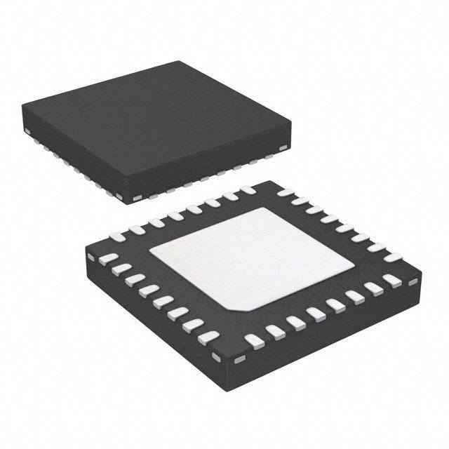
| 描述 | IC MODULATOR DIRECT QUAD 32-QFN |
| 产品分类 | |
| LO频率 | 100MHz ~ 5.6GHz |
| 品牌 | Hittite Microwave Corporation |
| 数据手册 | |
| 产品图片 |
|
| P1dB | 14dBm |
| 产品型号 | HMC795LP5E |
| RF频率 | 50MHz ~ 2.8GHz |
| rohs | 无铅 / 符合限制有害物质指令(RoHS)规范要求 |
| 产品系列 | - |
| 其它名称 | 1127-1571 |
| 功能 | 调制器 |
| 包装 | 散装 |
| 封装/外壳 | 32-VQFN 裸露焊盘 |
| 本底噪声 | -158dBm/Hz |
| 标准包装 | 50 |
| 测试频率 | - |
| 特色产品 | http://www.digikey.cn/product-highlights/zh/direct-iq-modulators/52283 |
| 电压-电源 | 4.5 V ~ 5.5 V |
| 电流-电源 | 127mA |
| 输出功率 | - |
| 配用 | /product-detail/zh/130186-HMC795LP5E/1127-2437-ND/4794728/product-detail/zh/129935-HMC795LP5E/1127-2436-ND/4794727/product-detail/zh/129934-HMC795LP5E/1127-2435-ND/4794726 |


- 商务部:美国ITC正式对集成电路等产品启动337调查
- 曝三星4nm工艺存在良率问题 高通将骁龙8 Gen1或转产台积电
- 太阳诱电将投资9.5亿元在常州建新厂生产MLCC 预计2023年完工
- 英特尔发布欧洲新工厂建设计划 深化IDM 2.0 战略
- 台积电先进制程称霸业界 有大客户加持明年业绩稳了
- 达到5530亿美元!SIA预计今年全球半导体销售额将创下新高
- 英特尔拟将自动驾驶子公司Mobileye上市 估值或超500亿美元
- 三星加码芯片和SET,合并消费电子和移动部门,撤换高东真等 CEO
- 三星电子宣布重大人事变动 还合并消费电子和移动部门
- 海关总署:前11个月进口集成电路产品价值2.52万亿元 增长14.8%


PDF Datasheet 数据手册内容提取
HMC795LP5E v00.0409 SiGe Wideband direct Quadrature Modulator w/ vGa, 50 - 2800 MHz typical applications Features the HMC795lP5e is ideal for: High linearity OiP3: + 22 dBm • uMts, GsM or CdMA Basestations High Output Power: +10 dBm Output P1dB • Fixed Wireless or Wll High Carrier suppression: 55 dBc • isM transceivers, 900 & 2400 MHz High sideband suppression: 53 dBc • GMsK, qPsK, qAM, ssB Modulators Read/Write serial Port interface (sPi) • Cellular/3G and WiMAX/4G sPi & 6-bit parallel port programmable 32 dB Gain Control • Microwave iFs 10 dC - 440 MHz Baseband input 32 lead 5x5 mm qFN Package: 25 mm2 Functional diagram General description t the HMC795lP5e is a variable gain, direct quadrature M modulator ideal for digital modulation applications s from 50 - 2800 MHz including: Cellular/3G, Broadband - Wireless Access and isM circuits. Housed in a compact e 5x5mm (lP5) sMt qFN package, the modulator R offers a high level of integration, exceptionally low u carrier feedthrough, and a low cost alternative to more t complicated double upconversion architectures. A the lO requires -9 to +3 dBm and can be driven R in either differential or single-ended mode. the d baseband inputs will support modulation inputs from A dC - 440 MHz. u the differential RF output port is driven by a 6 bit q digital controlled variable gain amplifier to nominally t provide up to 32 dB of very linear gain control in 0.5 dB C steps. the low carrier suppression is maintained over e the VGA dynamic range. the gain control interface R accepts either three wire serial input or 6 bit parallel i word. in addition, the gain control can be modified d through the sPi to adjust a look up table to control the - gain step to as low as 0.1 dB, with reduced range, or s to adjust individual gain steps for system linearization. R electrical Specifications, See test conditions on Following Page O t Parameter Min. typ. Max. Min. typ. Max. Min. typ. Max. units A RF Frequency 1000 1950 2690 MHz l Output Power 8 9.5 11 7 9 11 4 8 11 dB u Output P1dB 13 14 9 11 9 11 dBm d Output iP3 23 25 18 22 17 22 dBm O Carrier Feedthrough (uncal) -40 -45 -42 -46 -42 -46 dBm M Carrier Feedthrough (Cal) -55 -62 -55 -62 -52 -57 dBm sideband suppression (uncal) 43 55 49 53 45 50 dBc Output Noise Floor @ 20 MHz offset -158 -157 -156 -155 -154 -153 dBm/Hz RF Return loss -10 -14 -10 -12 -10 -12 dB lO Return loss -10 -15 -10 -15 -10 -12 dB Information furnisheFdo bry pAnraicloge ,D edviecelsiv ise rbyel,ie vaedn dto tboe apcclaurcatee aondr dreeliarbsle,. pHoleweavsere, n oc onFtoar cptr iHcei,t tditeeliv Meryic, raondw atov pel aCceo roprdoerras:t iAonna:log Devices, Inc., responsibility is assumed by Analog Devices for its use, nor for any infringements of patents or other One Technology Way, P.O. Box 9106, Norwood, MA 02062-9106 10 - 1 rliicgehntss eo fi sth girrda nptaerdti ebsy t hi2matp0 mlic aAayt iolrepns huolrta ofr tohRmer owitsias ueds eu,.n dSCepre hcainefiycl amptiaotsnesnf tos ourrb djpeac,t te Mtnot cArhiga hn0tgs1 eo 8wf Ai2thn4oaul otP gn oDhtiecovein.c eNeso.: 9P7h8o-n2e5: 708-13-332493-4 7 0F0a (cid:127)x O: r9d7e8r o-n2l5in0e -a3t w37w3w.analog.com Trademarks and registered trademarks are the property of their reOspercdtiever o wOnenrs-.line at www.hiAtptiptelic.actoiomn Support: Phone: 1-800-ANALOG-D
HMC795LP5E v00.0409 SiGe Wideband direct Quadrature Modulator w/ vGa, 50 - 2800 MHz electrical Specifications (Continued) Parameter Conditions Min. typ. Max. units Gain Control Characteristics Gain Control Range -31.5 0 dB Gain Control step Can be adjusted with sPi 0.5 dB state error (at max Attenuation) ±0.5 ±1 dB Gain step error ±0.05 ±0.13 dB RF Input Characteristics RF Frequency Range 50 2800 MHz RF Return loss Requires external matching 9 -15 -10 dB 10 RF Bandwidth with matching specified in table 5 10 15 % LO Input Characteristics lO Frequency Range 100 5600 MHz t lO Return loss Required 1 nF blocking cap -10 dB M lO drive level -9 0 +3 dBm s Baseband Inputs i/q input Bias level Output Power ±0.5 dB of typ. 1.2 1.3 1.4 V - input Bias Current 90 µA e R differential input impedance 5K||100pF Ohms||pF u Bandwidth dC 440 MHz t DC Power Requirements A Analog supply Voltage All must be equal 4.5 5 5.5 V R (VCCMiX, VCCBG, VCCRF, VCCdAC, VCClO) d digital supply Voltage (Vdd3) 3 3.3 3.5 V A idd - total Current Consumption 106 127 145 mA u Power down Current 1 µA q test conditions: unless otherwise Specified, the Following test conditions Were used t C Parameter Condition e temperature 25 °C R VGA Attenuation 0 dB i Baseband input Frequency 1 MHz d Baseband input dC Voltage 1.3V - Baseband input AC Voltage (Peak to Peak differential, i and q) 1.4V s Baseband input AC Voltage for OiP3 Measurement (Peak to Peak differential, i and q) 290 mV per tone @ 1 & 1.5 MHz R Frequency Offset for Output Noise Measurements 20 MHz O supply Analog: +5V, digital: +3.3V t lO input Power 0 dBm A lO input Mode differential l sideband and Carrier suppression uncalibrated u RF Output Mode differential d O M Information furnisheFdo bry pAnraicloge ,D edviecelsiv ise rbyel,ie vaedn dto tboe apcclaurcatee aondr dreeliarbsle,. pHoleweavsere, n oc onFtoar cptr iHcei,t tditeeliv Meryic, raondw atov pel aCceo roprdoerras:t iAonna:log Devices, Inc., responsibility is assumed by Analog Devices for its use, nor for any infringements of patents or other One Technology Way, P.O. Box 9106, Norwood, MA 02062-9106 rights of third parties th2at0 m aAy lrepshulta fr oRm oitsa udse,. SCpehcieficlamtiosnsf osurbdjec, t Mto cAha n0g1e 8wi2th4ou tP nohticoen. Neo: 9P7h8o-n2e5: 708-13-332493-4 7 0F0a (cid:127)x O: r9d7e8r o-n2l5in0e -a3t w37w3w.analog.com 10 - 2 license is granted by implication or otherwise under any patent or patent rights of Analog Devices. Trademarks and registered trademarks are the property of their reOspercdtiever o wOnenrs-.line at www.hiAtptiptelic.actoiomn Support: Phone: 1-800-ANALOG-D
HMC795LP5E v00.0409 SiGe Wideband direct Quadrature Modulator w/ vGa, 50 - 2800 MHz calibrated vs. uncalibrated test results during the uncalibrated Carrier suppression tests, care is taken to ensure that the i/q signal paths from the Vector signal Generator (VsG) to the device under test (dut) are equal. the “uncalibrated” Carrier suppression plots were measured at t= -40 °C, +25 °C, and +85 °C. the “Calibrated” Carrier suppression data was plotted after a manual adjustment of the iP/iN & qP/qN dC offsets at +25 °C, 5V Vcc, 0 dBm lO input power level, and the RF output frequency set to the midband of the measurement range. the adjustment settings were held constant during tests over temperature and frequency. 10 typical Performance characteristics, vcc +5v, lo 0 dbm, +25 °c t M s output Power, output iP3 & Sideband uncalibrated & calibrated carrier - Suppression vs. Freq. over temperature [1] Feedthrough vs. Freq. over temperature [1] e 40 0 -40 R m) UNCALIBRATED quAdRAtu TPUT POWER (dBm), OUTPUT IP3 (dB-123100000 OUTPUT IP3++ -284550 CCC SOIDUETBPAUNTD P OSUWPEPRRESSION -----5432100000SIDEBAND SUPPRESSION (dBc) CARRIER FEEDTHROUGH (dBm) -------77665545050505 CALIBR++ -284A550T ECCCD U O-20 -60 -80 t 800 850 900 950 1000 1050 1100 1150 1200 800 850 900 950 1000 1050 1100 1150 1200 C FREQUENCY (MHz) FREQUENCY (MHz) e carrier Feedthrough & Sideband R output Power & output noise @ 1 GHz vs. Suppression @ 1 GHz vs. vGa attenuation i d vGa attenuation over temperature [1] over temperature [1] - 20 -120 -50 -40 s -55 OdulAtOR OUTPUT POWER (dBm)---132100000 OUTPUT POWER OUTPUT N++ O-284I550S ECCC -----111117654300000OUTPUT NOISE @ 20 MHz (dBm/Hz) CARRIER FEEDTHROUGH (dBm)------887766505050 SFUESEPCIDDPAERTRBHERARSINESODRIUO GNH ++ -284550 CCC ---554505SIDEBAND SUPPRESSION (dBc) M -40 -180 -90 -60 0 4 8 12 16 20 24 28 32 0 4 8 12 16 20 24 28 32 ATTENUATION (dB) ATTENUATION (dB) [1] Output Matched to 1 GHz Information furnisheFdo bry pAnraicloge ,D edviecelsiv ise rbyel,ie vaedn dto tboe apcclaurcatee aondr dreeliarbsle,. pHoleweavsere, n oc onFtoar cptr iHcei,t tditeeliv Meryic, raondw atov pel aCceo roprdoerras:t iAonna:log Devices, Inc., responsibility is assumed by Analog Devices for its use, nor for any infringements of patents or other One Technology Way, P.O. Box 9106, Norwood, MA 02062-9106 10 - 3 rliicgehntss eo fi sth girrda nptaerdti ebsy t hi2matp0 mlic aAayt iolrepns huolrta ofr tohRmer owitsias ueds eu,.n dSCepre hcainefiycl amptiaotsnesnf tos ourrb djpeac,t te Mtnot cArhiga hn0tgs1 eo 8wf Ai2thn4oaul otP gn oDhtiecovein.c eNeso.: 9P7h8o-n2e5: 708-13-332493-4 7 0F0a (cid:127)x O: r9d7e8r o-n2l5in0e -a3t w37w3w.analog.com Trademarks and registered trademarks are the property of their reOspercdtiever o wOnenrs-.line at www.hiAtptiptelic.actoiomn Support: Phone: 1-800-ANALOG-D
HMC795LP5E v00.0409 SiGe Wideband direct Quadrature Modulator w/ vGa, 50 - 2800 MHz output Power & output noise carrier Feedthrough & Sideband @ 1 GHz vs. input baseband amplitude Suppression @ 1 GHz vs. input baseband over temperature [1] amplitude over temperature [1] 20 -145 -40 -40 OP1dB 14.3 dBm CARRIER UT POWER (dBm) 11055 O++ -284U550T CCCPUT POWOOEPPR11ddBB 1144..10 ddBBmm -150 OUTPUT NOISE @ 20 M FEEDTHROUGH (dBm) ---554505 FEEDTHROUGSHIDEBAND ---554505 SIDEBAND SUPPRE OUTP -05 OUTPUT NOISE -155 Hz (dBm/Hz) CARRIER --6650 ++ -284550 CCC SUPPRESSION --6650 SSION (dBc) 10 -10 -160 -70 -70 0.1 1 2 3 0.1 1 2 3 INPUT BASEBAND AMPLITUDE (Vp-p diff) INPUT BASEBAND AMPLITUDE (Vp-p diff) t M output Power, output iP3 & Sideband uncalibrated & calibrated carrier s Suppression vs. Freq. over lo Power [1] Feedthrough vs. Freq. over lo Power [1] - e 40 0 -40 m) R B OUTPUT IP3 -45 TPUT POWER (dBm), OUTPUT IP3 (d-123100000 + -039 dddBBBmmm SOIDUETBPAUNTD P OSUWPEPRRESSION -----5432100000SIDEBAND SUPPRESSION (dBc) CARRIER FEEDTHROUGH (dBm) ------776655505050 UNCALIBRATE + -D039 dddBBBmmmCALIBRATED quAdRAtu U O-28000 850 900 950 1000 1050 1100 1150 120-060 -80800 850 900 950 1000 1050 1100 1150 1200 t FREQUENCY (MHz) FREQUENCY (MHz) C e R output Power, output iP3 & Sideband Sup- uncalibrated & calibrated carrier Feed- i d pression vs. Freq. over Supply voltage [1] through vs. Freq. over Supply voltage [1] - 40 0 -40 Bm) OUTPUT IP3 -45 s TPUT POWER (dBm), OUTPUT IP3 (d-123100000 455...505VVV SOIDUETBPAUNTD P OSUWPEPRRESSION -----5432100000SIDEBAND SUPPRESSION (dBc) CARRIER FEEDTHROUGH (dBm) ------776655505050 UNCALIBRATED455...505 VVVCALIBRATED OdulAtOR U O-20 -60 -80 M 800 850 900 950 1000 1050 1100 1150 1200 800 850 900 950 1000 1050 1100 1150 1200 FREQUENCY (MHz) FREQUENCY (MHz) [1] Output Matched to 1 GHz Information furnisheFdo bry pAnraicloge ,D edviecelsiv ise rbyel,ie vaedn dto tboe apcclaurcatee aondr dreeliarbsle,. pHoleweavsere, n oc onFtoar cptr iHcei,t tditeeliv Meryic, raondw atov pel aCceo roprdoerras:t iAonna:log Devices, Inc., responsibility is assumed by Analog Devices for its use, nor for any infringements of patents or other One Technology Way, P.O. Box 9106, Norwood, MA 02062-9106 rights of third parties th2at0 m aAy lrepshulta fr oRm oitsa udse,. SCpehcieficlamtiosnsf osurbdjec, t Mto cAha n0g1e 8wi2th4ou tP nohticoen. Neo: 9P7h8o-n2e5: 708-13-332493-4 7 0F0a (cid:127)x O: r9d7e8r o-n2l5in0e -a3t w37w3w.analog.com 10 - 4 license is granted by implication or otherwise under any patent or patent rights of Analog Devices. Trademarks and registered trademarks are the property of their reOspercdtiever o wOnenrs-.line at www.hiAtptiptelic.actoiomn Support: Phone: 1-800-ANALOG-D
HMC795LP5E v00.0409 SiGe Wideband direct Quadrature Modulator w/ vGa, 50 - 2800 MHz output Power, output iP3 & Sideband uncalibrated & calibrated carrier Suppression vs. Freq. over temperature [1] Feedthrough vs. Freq. over temperature [1] 40 0 -40 m) UNCALIBRATED B +25 C -45 dBm), OUTPUT IP3 (d123000 OUTPUT IP3 OUTPUT POWER+ -8450 CC ---321000SIDEBAND SUPPR DTHROUGH (dBm) ---655050 WER ( 0 -40ESSIO R FEE -65 CALIBRATED 10 PUT PO-10 SIDEBAND SUPPRESSION -50N (dBc) CARRIE --7750 ++ -284550 CCC T U O-20 -60 -80 1800 1850 1900 1950 2000 2050 2100 2150 2200 1800 1850 1900 1950 2000 2050 2100 2150 2200 FREQUENCY (MHz) FREQUENCY (MHz) t carrier Feedthrough & Sideband M output Power & output noise @ 1950 MHz Suppression @ 1950 MHz vs. vGa s vs. vGa attenuation MHz over temperature [1] attenuation over temperature [1] - 20 -120 -50 -40 e quAdRAtuR OUTPUT POWER (dBm)---132100000 OUTPUT POWER OUTPUT N++ -O284I550S CCCE -----111117654300000OUTPUT NOISE @20MHz (dBm/Hz) CARRIER FEEDTHROUGH (dBm)-------88776655050505 SUSPIDPERBEASNSDIFO ENECDATRHRRIEORU GH ++ -284550 CCC ---554505SIDEBAND SUPPRESSION (dBc) -40 -180 -90 -60 t 0 4 8 12 16 20 24 28 32 0 4 8 12 16 20 24 28 32 C ATTENUATION (dB) ATTENUATION (dB) output Power & output noise carrier Feedthrough & Sideband e R @ 1950 MHz vs. input baseband Suppression @ 1950 MHz vs. input i amplitude over temperature [1] baseband amplitude over temperature [1] d 20 -140 -40 -30 - OP1dB 10.9 dBm CARRIER s 15 ++2855 CC OOPP11ddBB 1111..68 ddBBmm OUT Bm) -45 FEEDTHROUGH -35 S dulAtOR OUTPUT POWER (dBm) -11-00055 O U-4T0P CUT POWER OUTPUT NOISE ---111554505 PUT NOISE @ 20 MHz (dBm/H CARRIER FEEDTHROUGH (d ----66555050 +25 C SUSPIDPERBEASNSDIO N ----55445050 IDEBAND SUPPRESSION (dB O -15 z) + -8450 CC c) M -20 -160 -70 -60 0.1 1 2 3 0.1 1 2 3 INPUT BASEBAND AMPLITUDE (Vp-p diff) INPUT BASEBAND AMPLITUDE (Vp-p diff) [1] Output Matched to 1950 MHz Information furnisheFdo bry pAnraicloge ,D edviecelsiv ise rbyel,ie vaedn dto tboe apcclaurcatee aondr dreeliarbsle,. pHoleweavsere, n oc onFtoar cptr iHcei,t tditeeliv Meryic, raondw atov pel aCceo roprdoerras:t iAonna:log Devices, Inc., responsibility is assumed by Analog Devices for its use, nor for any infringements of patents or other One Technology Way, P.O. Box 9106, Norwood, MA 02062-9106 10 - 5 rliicgehntss eo fi sth girrda nptaerdti ebsy t hi2matp0 mlic aAayt iolrepns huolrta ofr tohRmer owitsias ueds eu,.n dSCepre hcainefiycl amptiaotsnesnf tos ourrb djpeac,t te Mtnot cArhiga hn0tgs1 eo 8wf Ai2thn4oaul otP gn oDhtiecovein.c eNeso.: 9P7h8o-n2e5: 708-13-332493-4 7 0F0a (cid:127)x O: r9d7e8r o-n2l5in0e -a3t w37w3w.analog.com Trademarks and registered trademarks are the property of their reOspercdtiever o wOnenrs-.line at www.hiAtptiptelic.actoiomn Support: Phone: 1-800-ANALOG-D
HMC795LP5E v00.0409 SiGe Wideband direct Quadrature Modulator w/ vGa, 50 - 2800 MHz output Power, output iP3 & Sideband uncalibrated & calibrated carrier Suppression vs. Freq. over lo Power [1] Feedthrough vs. Freq. over lo Power [1] 40 0 -40 m) B OUTPUT IP3 0 dBm -45 OUTPUT IP3 (d2300 OUTPUT POWER + -39 ddBBmm --2100SIDEBAND S OUGH (dBm) --5550 CUANLCIBARLAIBTREADTED WER (dBm), 100 --4300UPPRESSIO R FEEDTHR --6650 PUT PO-10 SIDEBAND SUPPRESSION -50N (dBc) CARRIE --7750 + -039 dddBBBmmm 10 T U O-20 -60 -80 1800 1850 1900 1950 2000 2050 2100 2150 2200 1800 1850 1900 1950 2000 2050 2100 2150 2200 FREQUENCY (MHz) FREQUENCY (MHz) t M output Power, output iP3 & Sideband Sup- uncalibrated & calibrated carrier Feed- s pression vs. Freq. over Supply voltage [1] through vs. Freq. over Supply voltage [1] - 40 0 -40 m) e B -45 TPUT POWER (dBm), OUTPUT IP3 (d-123100000 OUTPOUUT TPPOUWT455 EI...P505RVVV3 SIDEBAND SUPPRESSION -----5432100000SIDEBAND SUPPRESSION (dBc) CARRIER FEEDTHROUGH (dBm) ------776655505050 UNCALCIABLRIABTREADTED455...505 VVV quAdRAtuR U O-20 -60 -80 1800 1850 1900 1950 2000 2050 2100 2150 2200 1800 1850 1900 1950 2000 2050 2100 2150 2200 t FREQUENCY (MHz) FREQUENCY (MHz) C e output Power, output iP3 & Sideband uncalibrated & calibrated carrier R Suppression vs. Freq. over temperature [2] Feedthrough vs. Freq. over temperature [2] i d 40 10 -30 OUTPUT IP3 - 30 0 -35 s POWER (dBm) & IP3 (dBm)---12321000000 ++ -284550 CCC OUTPUSTI DPOEBWAENRD SUPPRESSION ------654321000000SIDEBAND SUPPRESSION (dBc) CARRIER FEEDTHROUGH (dBm) ----55445050 UCN++ AC-284LA550ILB CCCIRBARTAETDED OdulAtOR -40 -70 -60 M 2500 2550 2600 2650 2700 2750 2800 2500 2550 2600 2650 2700 2750 2800 FREQUENCY (MHz) FREQUENCY (MHz) [1] Output Matched to 1950 MHz [2] Output Matched to 2690 MHz Information furnisheFdo bry pAnraicloge ,D edviecelsiv ise rbyel,ie vaedn dto tboe apcclaurcatee aondr dreeliarbsle,. pHoleweavsere, n oc onFtoar cptr iHcei,t tditeeliv Meryic, raondw atov pel aCceo roprdoerras:t iAonna:log Devices, Inc., responsibility is assumed by Analog Devices for its use, nor for any infringements of patents or other One Technology Way, P.O. Box 9106, Norwood, MA 02062-9106 rights of third parties th2at0 m aAy lrepshulta fr oRm oitsa udse,. SCpehcieficlamtiosnsf osurbdjec, t Mto cAha n0g1e 8wi2th4ou tP nohticoen. Neo: 9P7h8o-n2e5: 708-13-332493-4 7 0F0a (cid:127)x O: r9d7e8r o-n2l5in0e -a3t w37w3w.analog.com 10 - 6 license is granted by implication or otherwise under any patent or patent rights of Analog Devices. Trademarks and registered trademarks are the property of their reOspercdtiever o wOnenrs-.line at www.hiAtptiptelic.actoiomn Support: Phone: 1-800-ANALOG-D
HMC795LP5E v00.0409 SiGe Wideband direct Quadrature Modulator w/ vGa, 50 - 2800 MHz carrier Feedthrough & Sideband output Power & output noise @ 2690 MHz Suppression @ 2960 MHz vs. vGa vs. vGa attenuation over temperature [1] attenuation over temperature [1] 20 -120 -10 -30 SIDEBAND +25C SUPPRESSION 10 + -8450CC -130 OUT Bm) -20 -40 S OWER (dBm) -100 OUTPUT POWER --115400 PUT NOISE @ DTHROUGH (d --4300 FEECDATRHRRIEORU GH --6500 IDEBAND SUP 10 OUTPUT P --3200 OUTPUT NOISE --117600 20 MHz (dBm/Hz) CARRIER FEE ---765000 ++ -284550 CCC ---987000 PRESSION (dBc) -40 -180 -80 -100 0 4 8 12 16 20 24 28 32 0 4 8 12 16 20 24 28 32 ATTENUATION (dB) ATTENUATION (dB) t output Power & output noise carrier Feedthrough & Sideband M @ 2960 MHz vs. input baseband Suppression @ 2960 MHz vs. input base- s amplitude over temperature [1] band amplitude over temperature [1] - 20 -135 -30 -20 e OP1dB 11.1 dBm +25 C R +85 C OP1dB 11.9 dBm O quAdRAtu OUTPUT POWER (dBm) -11000 OUTPU -T40 P COWEROP1dB 12.3 dBm ---111544050 UTPUT NOISE @ 20 MHz (dBm/Hz) CARRIER FEEDTHROUGH (dBm) ---654000 ++2855 CC FEECSDAUSTRPHIRDPRIEREOBERUAS GNSHDIO N ---543000 SIDEBAND SUPPRESSION (dBc) OUTPUT NOISE -40 C -20 -155 -70 -60 t 0.1 1 2 3 0.1 1 2 3 C INPUT BASEBAND AMPLITUDE (Vp-p diff) INPUT BASEBAND AMPLITUDE (Vp-p diff) e R output Power, output iP3 & Sideband uncalibrated & calibrated carrier i Suppression vs. Freq. over lo Power [1] Feedthrough vs. Freq. over lo Power [1] d 40 0 -30 OdulAtORs - TPUT POWER (dBm), OUTPUT IP3 (dBm) -123100000 OUTPUT IP3 OSUIDTEPBUATN PDO SWUEPRPRESSION + -039 dddBBBmmm -----5432100000 SIDEBAND SUPPRESSION (dBc) CARRIER FEEDTHROUGH (dBm) -----5544350505 UCNACLAIBLIRBARTAETDED + -039 dddBBBmmm U M O -20 -60 -60 2500 2550 2600 2650 2700 2750 2800 2500 2550 2600 2650 2700 2750 2800 FREQUENCY (MHz) FREQUENCY (MHz) [1] Output Matched to 2960 MHz Information furnisheFdo bry pAnraicloge ,D edviecelsiv ise rbyel,ie vaedn dto tboe apcclaurcatee aondr dreeliarbsle,. pHoleweavsere, n oc onFtoar cptr iHcei,t tditeeliv Meryic, raondw atov pel aCceo roprdoerras:t iAonna:log Devices, Inc., responsibility is assumed by Analog Devices for its use, nor for any infringements of patents or other One Technology Way, P.O. Box 9106, Norwood, MA 02062-9106 10 - 7 rliicgehntss eo fi sth girrda nptaerdti ebsy t hi2matp0 mlic aAayt iolrepns huolrta ofr tohRmer owitsias ueds eu,.n dSCepre hcainefiycl amptiaotsnesnf tos ourrb djpeac,t te Mtnot cArhiga hn0tgs1 eo 8wf Ai2thn4oaul otP gn oDhtiecovein.c eNeso.: 9P7h8o-n2e5: 708-13-332493-4 7 0F0a (cid:127)x O: r9d7e8r o-n2l5in0e -a3t w37w3w.analog.com Trademarks and registered trademarks are the property of their reOspercdtiever o wOnenrs-.line at www.hiAtptiptelic.actoiomn Support: Phone: 1-800-ANALOG-D
HMC795LP5E v00.0409 SiGe Wideband direct Quadrature Modulator w/ vGa, 50 - 2800 MHz output Power, output iP3 & Sideband Sup- uncalibrated & calibrated carrier Feed- pression vs. Freq. over Supply voltage [1] through vs. Freq. over Supply voltage [1] 40 0 -30 OUTPUT IP3 4.5V 5.0V POWER (dBm) & IP3 (dBm) -123100000 OUTPUT POWSEIRDEBAND SUPPRESSION 5.5V -----5432100000 SIDEBAND SUPPRESSION (dBc) CARRIER FEEDTHROUGH (dBm) -----5544350505 UNCCAALLIIBBRRAATTEEDD 455...505 VVV 10 -20 -60 -60 2500 2550 2600 2650 2700 2750 2800 2500 2550 2600 2650 2700 2750 2800 FREQUENCY (MHz) FREQUENCY (MHz) t M normalized attenuation vs. Frequency absolute error [2] vs. Frequency s (only Major States are Shown) (Only Major States are Shown) 0 1 - e -5 R B) UATION (d --1150 OR (dB) 0.5 Atu MALIZED ATTEN --2250 ABSOLUTE ERR -0.50 uAdR R O -30 N q -35 -1 0 0.5 1 1.5 2 2.5 0 0.5 1 1.5 2 2.5 t FREQUENCY (GHz) FREQUENCY (GHz) C e Step error [3] vs. Frequency R absolute error [2] vs. attenuation State (Only Major States are Shown) i d 0.5 0.5 - s 0.25 0.25 R OLUTE ERROR (dB) 0 2251. 0 5GG MGHHHzHzzz STEP ERROR (dB) 0 ulAtO ABS-0.25 -0.25 d O -0.5 -0.5 M 0 4 8 12 16 20 24 28 32 0 0.5 1 1.5 2 2.5 ATTENUATION (dB) FREQUENCY (GHz) [1] Output Matched to 2960 MHz [2] Absolute error - difference between measured and ideal attenuation [3] step error - difference between measured attuation step and ideal step of 0.5 dB Information furnisheFdo bry pAnraicloge ,D edviecelsiv ise rbyel,ie vaedn dto tboe apcclaurcatee aondr dreeliarbsle,. pHoleweavsere, n oc onFtoar cptr iHcei,t tditeeliv Meryic, raondw atov pel aCceo roprdoerras:t iAonna:log Devices, Inc., responsibility is assumed by Analog Devices for its use, nor for any infringements of patents or other One Technology Way, P.O. Box 9106, Norwood, MA 02062-9106 rights of third parties th2at0 m aAy lrepshulta fr oRm oitsa udse,. SCpehcieficlamtiosnsf osurbdjec, t Mto cAha n0g1e 8wi2th4ou tP nohticoen. Neo: 9P7h8o-n2e5: 708-13-332493-4 7 0F0a (cid:127)x O: r9d7e8r o-n2l5in0e -a3t w37w3w.analog.com 10 - 8 license is granted by implication or otherwise under any patent or patent rights of Analog Devices. Trademarks and registered trademarks are the property of their reOspercdtiever o wOnenrs-.line at www.hiAtptiptelic.actoiomn Support: Phone: 1-800-ANALOG-D
HMC795LP5E v00.0409 SiGe Wideband direct Quadrature Modulator w/ vGa, 50 - 2800 MHz Step error vs. attenuation rF return loss vs. attenuation 0.15 0 0.1 -5 0.05 B) -10 EP ERROR (dB)-0.050 ETURN LOSS (d --2105 12060900MMHHzz ST F R 50 MHz, 1 GHz, 2 GHz, 2.5 GHz R 10 -0.1 -25 1950 MHz -0.15 -30 0 4 8 12 16 20 24 28 32 0 4 8 12 16 20 24 28 32 ATTENUATION (dB) ATTENUATION STATE (dB) t M rF return loss vs. Frequency offset, s lo return loss vs. Frequency vGa attenuation 0 db - 0 0 e 1000MHz R -5 u -10 dRAt ETURN LOSS (dB) -20 RETURN LOSS (dB) ---211050 2690MHz A R -30 1950MHz u SINGLE-ENDED LO -25 DIFFERENTIAL LO q WITH BD2326 BALUN -40 -30 0 1 2 3 4 5 -150 -100 -50 0 50 100 150 t FREQUENCY (GHz) OFFSET FREQUENCY (MHz) C e acPr for W-cdMa @ 2140 MHz acPr for W-cdMa @ 2140 MHz R vs. output Power for various input levels, vs. output Power & vGa attenuation for i vGa attenuation 0 db [1] various input levels [1] d -50 -30 -60 - s -55 -40 ACPR 0 dB -80 OUT R ADJACENT CH. PU O ACPR -50 31.5dB 110mV (rms) -100 T NO t dBc) -60 R (dB) -60 31.5dB 65mV (rms) 0 dB -120 ISE @ lA ACPR ( -65 ACP -70 37mV (rms) 0 dB -140 20 MH u ALTERNATE CH. z (d d -70 ACPR -80 0 dB -160 Bm/H 28dB z) O OUTPUT NOISE -75 -90 -180 M -15 -10 -5 0 -40 -30 -20 -10 0 10 CARRIER OUTPUT POWER (dBm) CARRIER OUTPUT POWER (dBm) [1] W-CdMA (Modulation set-up for ACPR Mode): the baseband i and q input signals were generated using “test Model 1 with 64 channels Information furnisheFdo bry pAnraicloge ,D edviecelsiv ise rbyel,ie vaedn dto tboe apcclaurcatee aondr dreeliarbsle,. pHoleweavsere, n oc onFtoar cptr iHcei,t tditeeliv Meryic, raondw atov pel aCceo roprdoerras:t iAonna:log Devices, Inc., responsibility is assumed by Analog Devices for its use, nor for any infringements of patents or other One Technology Way, P.O. Box 9106, Norwood, MA 02062-9106 10 - 9 rliicgehntss eo fi sth girrda nptaerdti ebsy t hi2matp0 mlic aAayt iolrepns huolrta ofr tohRmer owitsias ueds eu,.n dSCepre hcainefiycl amptiaotsnesnf tos ourrb djpeac,t te Mtnot cArhiga hn0tgs1 eo 8wf Ai2thn4oaul otP gn oDhtiecovein.c eNeso.: 9P7h8o-n2e5: 708-13-332493-4 7 0F0a (cid:127)x O: r9d7e8r o-n2l5in0e -a3t w37w3w.analog.com Trademarks and registered trademarks are the property of their reOspercdtiever o wOnenrs-.line at www.hiAtptiptelic.actoiomn Support: Phone: 1-800-ANALOG-D
HMC795LP5E v00.0409 SiGe Wideband direct Quadrature Modulator w/ vGa, 50 - 2800 MHz absolute Maximum ratings truth table VCCMiX, VCCBG, VCCRF, VCCdAC -0.3V to +5.5V Control Voltage input Attenuation Vdd3 -0.3V to +3.6V AGC5 AGC4 AGC3 AGC2 AGC1 AGC1 lO input Power +18 dBm low low low low low low 0 dB Baseband input Voltage (dC) 0V to +1.4V low low low low low High 0.5 dB Baseband input Voltage (AC + dC) 0V to +1.8V low low low low High low 1 dB Maximum Junction temperature 125 °C low low low High low low 2 dB Continuous Pdiss (t = 85°C) (derate 25 mW/°C above 85°C) 1W low low High low low low 4 dB thermal Resistance (R ) low High low low low low 8 dB th 40 °C/W (junction to ground paddle) High low low low low low 16 dB 10 storage temperature -65 to +150 °C High High High High High High 31.5 dB Operating temperature -40 to +85 °C Any combination of the above states will provide an increase in the Reflow soldering attenuation approximately equal to the sum of the bits selected Peak temperature 260 °C t esd sensitivity (HBM) Class 1B M eleCtROstAtiC seNsitiVe deViCe stresses above those listed under Absolute Maximum Ratings may s cause permanent damage to the device. this is a stress rating only; OBseRVe HANdliNG PReCAutiONs functional operation of the device at these or any other conditions - above those indicated in the operational section of this specification e is not implied. exposure to absolute maximum rating conditions for R extended periods may affect device reliability. u outline drawing t A R d A u q t C e R i d - s R NOtes: 1. leAdFRAMe MAteRiAl: COPPeR AllOY O 2. diMeNsiONs ARe iN iNCHes [MilliMeteRs] t 3. leAd sPACiNG tOleRANCe is NON-CuMulAtiVe. A 4. PAd BuRR leNGtH sHAll Be 0.15mm MAXiMuM. l PAd BuRR HeiGHt sHAll Be 0.05mm MAXiMuM. u 5. PACKAGe WARP sHAll NOt eXCeed 0.05mm. 6. All GROuNd leAds ANd GROuNd PAddle Must Be sOldeRed tO PCB RF GROuNd. d Package information 7. ReFeR tO Hittite APPliCAtiON NOte FOR suGGested lANd PAtteRN. O M Part Number Package Body Material lead Finish Msl Rating Package Marking [1] HMC795lP5e RoHs-compliant low stress injection Molded Plastic 100% matte sn Msl1 [2] H795 XXXX [1] 4-digit lot number XXXX [2] Max peak reflow temperature of 260 °C Information furnisheFdo bry pAnraicloge ,D edviecelsiv ise rbyel,ie vaedn dto tboe apcclaurcatee aondr dreeliarbsle,. pHoleweavsere, n oc onFtoar cptr iHcei,t tditeeliv Meryic, raondw atov pel aCceo roprdoerras:t iAonna:log Devices, Inc., responsibility is assumed by Analog Devices for its use, nor for any infringements of patents or other One Technology Way, P.O. Box 9106, Norwood, MA 02062-9106 rights of third parties th2at0 m aAy lrepshulta fr oRm oitsa udse,. SCpehcieficlamtiosnsf osurbdjec, t Mto cAha n0g1e 8wi2th4ou tP nohticoen. Neo: 9P7h8o-n2e5: 708-13-332493-4 7 0F0a (cid:127)x O: r9d7e8r o-n2l5in0e -a3t w37w3w.analog.com 10 - 10 license is granted by implication or otherwise under any patent or patent rights of Analog Devices. Trademarks and registered trademarks are the property of their reOspercdtiever o wOnenrs-.line at www.hiAtptiptelic.actoiomn Support: Phone: 1-800-ANALOG-D
HMC795LP5E v00.0409 SiGe Wideband direct Quadrature Modulator w/ vGa, 50 - 2800 MHz Pin descriptions Pin Number Function description interface schematic 1 RstB digital reset input, active low 10 supply voltage for the output driver, 2 VCCRF 5V, 24mA @ max gain, 0.7mA @ min gain t 3, 6, 19, 22 GNd these pins and the ground paddle should be connected to a high quality RF/dC ground. M s - e differential RF open collector output, needs pull up R 4, 5 RFN, RFP inductor to VCCRF and dC coupling capacitor on both u pins, 5V, 0.5mA @min gain, 24.4mA @ max gain t A R d A u q 7, 8, 9, 10, AGC0, AGC1, AGC2, AGC3, Parallel binary input gain control word 11, 12 AGC4, AGC5 t C e R i 13 VCCdAC supply voltage for the dAC, 3.9mA @ 5V d - s q channel differential baseband input. these high R 14, 15 qP, qN impedance ports should be biased at 1.3V. Nominal recommended baseband input is 1.4V pp differential O t A 16, 25 VCCMiX supply voltage for the i/q mixers, 31.7mA @ 5V l u the pins are not connected internally; however, all data 17 N/C shown herein was measured with these pins connected to d RF/dC ground externally. O 18 VCClO supply voltage for the lO chain, 65.2mA @ 5V M Information furnisheFdo bry pAnraicloge ,D edviecelsiv ise rbyel,ie vaedn dto tboe apcclaurcatee aondr dreeliarbsle,. pHoleweavsere, n oc onFtoar cptr iHcei,t tditeeliv Meryic, raondw atov pel aCceo roprdoerras:t iAonna:log Devices, Inc., responsibility is assumed by Analog Devices for its use, nor for any infringements of patents or other One Technology Way, P.O. Box 9106, Norwood, MA 02062-9106 10 - 11 rliicgehntss eo fi sth girrda nptaerdti ebsy t hi2matp0 mlic aAayt iolrepns huolrta ofr tohRmer owitsias ueds eu,.n dSCepre hcainefiycl amptiaotsnesnf tos ourrb djpeac,t te Mtnot cArhiga hn0tgs1 eo 8wf Ai2thn4oaul otP gn oDhtiecovein.c eNeso.: 9P7h8o-n2e5: 708-13-332493-4 7 0F0a (cid:127)x O: r9d7e8r o-n2l5in0e -a3t w37w3w.analog.com Trademarks and registered trademarks are the property of their reOspercdtiever o wOnenrs-.line at www.hiAtptiptelic.actoiomn Support: Phone: 1-800-ANALOG-D
HMC795LP5E v00.0409 SiGe Wideband direct Quadrature Modulator w/ vGa, 50 - 2800 MHz Pin descriptions (Continued) Pin Number Function description interface schematic lO inputs. Need dC decoupling capacitors. the ports 20, 21 lOP, lON could be driven single ended or differentially 10 23 VCCBG supply voltage for the bandgap, 4.3mA @ 5V external bypass decoupling for precision bias circuits, 3.80V t M 24 deCOuPle NOte: BiAs ref voltage cannot drive an external load. Must be measured with 10GOhm meter such as Agilent 34410A, s normal 10Mohm dVM will read erroneously. - e R i channel differential baseband input. these high u 26, 27 iN, iP impedance ports should be biased at 1.3V. Nominal recommended baseband input is 1.4V pp differential t A R 28 Vdd3 supply voltage for the digital d A u q 29 sdO Main serial port data output t C e R i d 30 sdi Main serial port data input - s R 31 seN Main serial port latch enable input O t A 32 sCK Main serial port clock input l u d O M Information furnisheFdo bry pAnraicloge ,D edviecelsiv ise rbyel,ie vaedn dto tboe apcclaurcatee aondr dreeliarbsle,. pHoleweavsere, n oc onFtoar cptr iHcei,t tditeeliv Meryic, raondw atov pel aCceo roprdoerras:t iAonna:log Devices, Inc., responsibility is assumed by Analog Devices for its use, nor for any infringements of patents or other One Technology Way, P.O. Box 9106, Norwood, MA 02062-9106 rights of third parties th2at0 m aAy lrepshulta fr oRm oitsa udse,. SCpehcieficlamtiosnsf osurbdjec, t Mto cAha n0g1e 8wi2th4ou tP nohticoen. Neo: 9P7h8o-n2e5: 708-13-332493-4 7 0F0a (cid:127)x O: r9d7e8r o-n2l5in0e -a3t w37w3w.analog.com 10 - 12 license is granted by implication or otherwise under any patent or patent rights of Analog Devices. Trademarks and registered trademarks are the property of their reOspercdtiever o wOnenrs-.line at www.hiAtptiptelic.actoiomn Support: Phone: 1-800-ANALOG-D
HMC795LP5E v00.0409 SiGe Wideband direct Quadrature Modulator w/ vGa, 50 - 2800 MHz evaluation Pcb 10 t M s - e R u t A R d A u q t C e R i d the circuit board used in the application should use RF circuit design techniques. signal lines should have - 50 ohm impedance while the package ground leads and exposed paddle should be connected directly to the s R ground plane similar to that shown. A sufficient number of via holes should be used to connect the top and O bottom ground planes. the evaluation circuit board shown is available from Hittite upon request. t A l u d O M Information furnisheFdo bry pAnraicloge ,D edviecelsiv ise rbyel,ie vaedn dto tboe apcclaurcatee aondr dreeliarbsle,. pHoleweavsere, n oc onFtoar cptr iHcei,t tditeeliv Meryic, raondw atov pel aCceo roprdoerras:t iAonna:log Devices, Inc., responsibility is assumed by Analog Devices for its use, nor for any infringements of patents or other One Technology Way, P.O. Box 9106, Norwood, MA 02062-9106 10 - 13 rliicgehntss eo fi sth girrda nptaerdti ebsy t hi2matp0 mlic aAayt iolrepns huolrta ofr tohRmer owitsias ueds eu,.n dSCepre hcainefiycl amptiaotsnesnf tos ourrb djpeac,t te Mtnot cArhiga hn0tgs1 eo 8wf Ai2thn4oaul otP gn oDhtiecovein.c eNeso.: 9P7h8o-n2e5: 708-13-332493-4 7 0F0a (cid:127)x O: r9d7e8r o-n2l5in0e -a3t w37w3w.analog.com Trademarks and registered trademarks are the property of their reOspercdtiever o wOnenrs-.line at www.hiAtptiptelic.actoiomn Support: Phone: 1-800-ANALOG-D
HMC795LP5E v00.0409 SiGe Wideband direct Quadrature Modulator w/ vGa, 50 - 2800 MHz list of Materials for evaluation Pcb [1] item description item description J1, J10 2 Pin dC Connector R7 10 kOhm Resistor, 0402 Pkg J2, J3, J5 - J8 PCB Mount sMA Connector R8, R9, R12 - R20, R22, R23, R25, R26, do Not Populate J4 12 Pin dC Connector R28, R29 J9 12 Pin socket Connector R10 4 kOhm Resistor, 0402 Pkg C1, C4, C8, C10, C14, C15, R11 1 kOhm Resistor, 0402 Pkg C18, C20, C23, C34, C35, 1 µF Capacitor, 0402 Pkg C38 t1, t2 RF transformer C2 10 µF Capacitor, 1206 Pkg tP1 - tP3 dC Pin 10 C3, C5, C6, C11, C12 4.7 µF Capacitor, 0805 Pkg FB1 - FB3 1 kOhms Ferrite Bead, 0805 Pkg C7, C16, C17, C22, C24, l1, l3 10 nH inductor, 0402 Pkg C25, C28, C33, C36, C37, 1 nF Capacitor, 0402 Pkg l2, l6 4.7 nH inductor, 0402 Pkg C40 t C9, C21 10 nF Capacitor, 0402 Pkg u1 linear Regulator, 3.3V M C13 1.2 nF Capacitor, 0402 Pkg u2 linear Regulator, 5V s u3 HMC795lP5e Modulator C19, C27, C32, C41 100 pF Capacitor, 0402 Pkg - C26, C30 - C31, C39, C42 do Not Populate PCB [2] 125087 eval Board e [1] When requesting an evaluation board, please reference the R R1, R4, R21, R24, R27, 100 kOhm Resistor, 0402 Pkg appropriate PCB number listed in the table “Components for the R30 - R32 u selected Frequencies” R2, R3, R5, R6 0 Ohm Resistor, 0402 Pkg t [2] Circuit Board Material: Arlon 25FR / FR4 A R d A u table 9. components for Selected Frequencies q tuned Frequency 850 MHz 1950 MHz 2960 MHz t evaluation Board Number 127433 125370 130190 C evaluation Kit Number [1] 129934 129935 130186 e l2, l6 47 nH 4.7 nH 1.8 nH R i l1, l3 27 nH 10 nH 5.6 nH d R29 2.5 kOhms dePOP dePOP - t1 tCN2-14 tCN2-26 tCN2-26 s [1] evaluation Kit includes evaluation board, usB controller board, usB cable and evaluation software. R O t A l u d O M Information furnisheFdo bry pAnraicloge ,D edviecelsiv ise rbyel,ie vaedn dto tboe apcclaurcatee aondr dreeliarbsle,. pHoleweavsere, n oc onFtoar cptr iHcei,t tditeeliv Meryic, raondw atov pel aCceo roprdoerras:t iAonna:log Devices, Inc., responsibility is assumed by Analog Devices for its use, nor for any infringements of patents or other One Technology Way, P.O. Box 9106, Norwood, MA 02062-9106 rights of third parties th2at0 m aAy lrepshulta fr oRm oitsa udse,. SCpehcieficlamtiosnsf osurbdjec, t Mto cAha n0g1e 8wi2th4ou tP nohticoen. Neo: 9P7h8o-n2e5: 708-13-332493-4 7 0F0a (cid:127)x O: r9d7e8r o-n2l5in0e -a3t w37w3w.analog.com 10 - 14 license is granted by implication or otherwise under any patent or patent rights of Analog Devices. Trademarks and registered trademarks are the property of their reOspercdtiever o wOnenrs-.line at www.hiAtptiptelic.actoiomn Support: Phone: 1-800-ANALOG-D
HMC795LP5E v00.0409 SiGe Wideband direct Quadrature Modulator w/ vGa, 50 - 2800 MHz application & evaluation Pcb Schematic 10 t M s - e R u t A R d A u q t C e R i d - s R O t A l u d O M Information furnisheFdo bry pAnraicloge ,D edviecelsiv ise rbyel,ie vaedn dto tboe apcclaurcatee aondr dreeliarbsle,. pHoleweavsere, n oc onFtoar cptr iHcei,t tditeeliv Meryic, raondw atov pel aCceo roprdoerras:t iAonna:log Devices, Inc., responsibility is assumed by Analog Devices for its use, nor for any infringements of patents or other One Technology Way, P.O. Box 9106, Norwood, MA 02062-9106 10 - 15 rliicgehntss eo fi sth girrda nptaerdti ebsy t hi2matp0 mlic aAayt iolrepns huolrta ofr tohRmer owitsias ueds eu,.n dSCepre hcainefiycl amptiaotsnesnf tos ourrb djpeac,t te Mtnot cArhiga hn0tgs1 eo 8wf Ai2thn4oaul otP gn oDhtiecovein.c eNeso.: 9P7h8o-n2e5: 708-13-332493-4 7 0F0a (cid:127)x O: r9d7e8r o-n2l5in0e -a3t w37w3w.analog.com Trademarks and registered trademarks are the property of their reOspercdtiever o wOnenrs-.line at www.hiAtptiptelic.actoiomn Support: Phone: 1-800-ANALOG-D
HMC795LP5E v00.0409 SiGe Wideband direct Quadrature Modulator w/ vGa, 50 - 2800 MHz Theory of Operation the HMC795lP5e modulator consists of the following functional blocks 1. lO interface 2. i/q modulator 3. digitally controlled variable gain amplifier 4. Gain control dAC 5. Bias Circuit 6. serial Port interface lo interface 10 the lO interface consists of a gain stage followed by a divide by 2 stage that generates two carrier signals in quad- rature which are used to drive the mixers. As a result, the lO path is immune to large variations in the lO signal level and the modulator performance does not vary much with lO power. due to the on chip divider, the input lO frequency must be twice that of the desired carrier frequency. this offers the advantage of significantly lowering t carrier feedthrough. M the lO port can be driven differentially or single ended if the unused side is AC grounded. However, when driven s single-endedly, the carrier feedthrough and sideband rejection can be degraded by either large 2nd order lO tones, - such as when driven by a VCO with a divider output, or, by large half-harmonic tones, such as when driven by a VCO e with a doubler output. R the lO interface can be enabled/disabled separately through the serial port interface using Reg01h <0> and can be u used to disable the modulator output. the RF output signal is suppressed by 100 dB when only the lO interface is t disable and the lO signal itself is suppressed approximately 60 dB. in addition, the lO buffer bias can be increased A using Reg02h <7>. this setting is recommended for lO frequencies above 5 GHz. R d i/Q Modulator A u the HMC795lP5e has two double-balanced mixers, one for the in-phase channel and one for the quadrature chan- q nel. the differential baseband inputs (qP, qN, iP, and iN) consist of the bases of NPN transistors, which present a high impedance. the dC common mode voltage at the baseband inputs sets the currents in the two mixer cores. t Varying the baseband common mode voltage varies the current in the mixers and affects the overall modulators C performance. the recommended dC voltage for the baseband common mode voltage is 1.3V dC, ± 0.1V. e R the output of the two mixers are summed together differentially and then used to drive the differential input of the VGA i stage. the mixer can be enabled/disabled with Reg01h <1>. the external baseband dC bias also need to be disabled d to completely disable the mixers. disabling the mixer enables a weak pull down at the mixer inputs which connects - the mixer inputs through a resistive path to ground. this may pull the external input low resulting in large current flow s if the external bias is not disabled. R O t A l u d O M Information furnisheFdo bry pAnraicloge ,D edviecelsiv ise rbyel,ie vaedn dto tboe apcclaurcatee aondr dreeliarbsle,. pHoleweavsere, n oc onFtoar cptr iHcei,t tditeeliv Meryic, raondw atov pel aCceo roprdoerras:t iAonna:log Devices, Inc., responsibility is assumed by Analog Devices for its use, nor for any infringements of patents or other One Technology Way, P.O. Box 9106, Norwood, MA 02062-9106 rights of third parties th2at0 m aAy lrepshulta fr oRm oitsa udse,. SCpehcieficlamtiosnsf osurbdjec, t Mto cAha n0g1e 8wi2th4ou tP nohticoen. Neo: 9P7h8o-n2e5: 708-13-332493-4 7 0F0a (cid:127)x O: r9d7e8r o-n2l5in0e -a3t w37w3w.analog.com 10 - 16 license is granted by implication or otherwise under any patent or patent rights of Analog Devices. Trademarks and registered trademarks are the property of their reOspercdtiever o wOnenrs-.line at www.hiAtptiptelic.actoiomn Support: Phone: 1-800-ANALOG-D
HMC795LP5E v00.0409 SiGe Wideband direct Quadrature Modulator w/ vGa, 50 - 2800 MHz digitally controlled variable Gain amplifier the output of the HMC795lP5e is a 6 bit, digitally controlled, variable gain amplifier that can provide very accurate linear- in-dB gain control over a 31.5 dB range in 0.5 dB steps. the VGA also provides relatively constant phase over the entire gain range, as shown in Figure 1. An 11 bit dAC is used to control the VGA. see the Gain Control dAC section for more detail about gain control. 10 -50 5 -60 0 -70 B) 10 GNITUDE (d-1-05 MAGNITUDE PHASE --9800 S21 PHASE 1 MA-15 -100 (deg S2-20 -110 ) t M -25 -120 s -30 -130 0 4 8 12 16 20 24 28 32 - ATTENUATION (dB) e Figure 1. VGA S21 magnitude and phase @ 2 GHz vs attenuation R u t For maximum performance and flexibility, the output ports of the VGA are differential open collectors that require A pull up inductors to the positive supply and external matching components. the evaluation board allows for several R options for matching. see the Output Matching section for more details. d the VGA can be enabled/disabled separately through the sPi using Reg01h <2>. the ON/OFF isolation of the VGA A is greater than 60 dB for RF output frequencies up to 2.5 GHz. u q Gain control dac t An 11 bit dAC is used to control the VGA for linear-in-dB gain control, Figure 2 shows the control for the dAC.. the C dAC is normally controlled by a look up table (lut) that is in turn, controlled by the 6 bit parallel port. the values of e the look up table are fixed to give 0.5 dB steps over a 31.5 dB gain range. R i d - s R O t A Figure 2. Simplified DAC control diagram l For increased flexibility, there are three methods to control the dAC and VGA gain. u d 1. Parallel Mode use the 6 bit parallel port to provide fixed 0.5 dB gain steps. in this mode the dAC is controlled by a look up table with 64 states that map the 6 bit parallel port to fixed 11-Bit gain O words for each state. the values of the lut are fixed to give nominally 0.5 dB attenuation steps M over a 31.5 dB gain range. Information furnisheFdo bry pAnraicloge ,D edviecelsiv ise rbyel,ie vaedn dto tboe apcclaurcatee aondr dreeliarbsle,. pHoleweavsere, n oc onFtoar cptr iHcei,t tditeeliv Meryic, raondw atov pel aCceo roprdoerras:t iAonna:log Devices, Inc., responsibility is assumed by Analog Devices for its use, nor for any infringements of patents or other One Technology Way, P.O. Box 9106, Norwood, MA 02062-9106 10 - 17 rliicgehntss eo fi sth girrda nptaerdti ebsy t hi2matp0 mlic aAayt iolrepns huolrta ofr tohRmer owitsias ueds eu,.n dSCepre hcainefiycl amptiaotsnesnf tos ourrb djpeac,t te Mtnot cArhiga hn0tgs1 eo 8wf Ai2thn4oaul otP gn oDhtiecovein.c eNeso.: 9P7h8o-n2e5: 708-13-332493-4 7 0F0a (cid:127)x O: r9d7e8r o-n2l5in0e -a3t w37w3w.analog.com Trademarks and registered trademarks are the property of their reOspercdtiever o wOnenrs-.line at www.hiAtptiptelic.actoiomn Support: Phone: 1-800-ANALOG-D
HMC795LP5E v00.0409 SiGe Wideband direct Quadrature Modulator w/ vGa, 50 - 2800 MHz 2. Correction Mode use the sPi port in conjunction with the 6 bit parallel port to apply a 4 bit, 2’s complement, correction factor to any attenuation step. this option can be used to compensate the gain control for systematic variations in the transmit chain by adding negative or positive correction factors to any of the fixed lut values to either slightly increase or decrease the gain step for that particulate state. this mode requires the host controller to write the desired corrections to the sPi after the chip is powered up. the correction factors are then applied to the desired gain steps when ever the parallel port gain control changes, until the chip is powered down. the 4 bit, 2’s compliment, correction factor for each line in the lut are set by Reg4h to Reg13h. the correction factor for 0 dB attenuation (line 0) is set in Reg4h <3:0>, 0.5 dB (line 1) is set by Reg4h <7:4>, 1.0 dB (line 2) by Reg4h<11:8> and so on until Reg13h <15:12> which sets the correc- 10 tion factor for 31.5 dB attenuation. if more adjustment is needed, the lut correction values can be increased by a factor of 2, 3, or 4 times by using Reg2h <15:8>. Reg2h <9:8> sets the multiplication factor for the first quadrant of the lut, lines 0 to 15, <11:10> for lines 16 to 31, <13:12> for lines 32 to 47 and <15:14> for the last quadrant, lines 48 to 63. the correction in dB can be estimated by t [( (C O R w or d · m u lt ))-1 ] M COR(dB) = 10 · log10 1 + LUTword s - where mult is the correction multiplication factor, and CORword and lutword are the decimal equivalent e of the binary correction and lut word. An expression for determining the lutword is given in the bypass R mode section below. Figures 3, 4 and 5 show the range of correction in dB for 4 dB, 16 dB and 31.5 dB u attenuation and Figure 6 shows the output power versus attenuation for no correction, maximum positive t and maximum negative correction applied to all states in the lut. the lut value for 0 dB attenuation can A only be decreased since it already at maximum. increasing the word value will cause an overflow resulting R in maximum attenuation instead. d 0.3 1 A u 0.2 X4 X4 B) X3 B) 0.5 X3 q GE (d 0.1 X1X2 GE (d X1X2 t N N CHA 0 CHA 0 C ON ON e UATI -0.1 UATI R ATTEN -0.2 ATTEN -0.5 di - -0.3 -1 -8 -6 -4 -2 0 2 4 6 8 -8 -6 -4 -2 0 2 4 6 8 s LUT CORRECTION WORD LUT CORRECTION WORD R Figure 3. Attenuation Change from 4 dB Attenuation Figure 4. Attenuation Change from 16 dB Attenuation O vs. LUT Correction Word over Different vs. LUT Correction Word over Different t Multiplication Factors Multiplication Factors A l u d O M Information furnisheFdo bry pAnraicloge ,D edviecelsiv ise rbyel,ie vaedn dto tboe apcclaurcatee aondr dreeliarbsle,. pHoleweavsere, n oc onFtoar cptr iHcei,t tditeeliv Meryic, raondw atov pel aCceo roprdoerras:t iAonna:log Devices, Inc., responsibility is assumed by Analog Devices for its use, nor for any infringements of patents or other One Technology Way, P.O. Box 9106, Norwood, MA 02062-9106 rights of third parties th2at0 m aAy lrepshulta fr oRm oitsa udse,. SCpehcieficlamtiosnsf osurbdjec, t Mto cAha n0g1e 8wi2th4ou tP nohticoen. Neo: 9P7h8o-n2e5: 708-13-332493-4 7 0F0a (cid:127)x O: r9d7e8r o-n2l5in0e -a3t w37w3w.analog.com 10 - 18 license is granted by implication or otherwise under any patent or patent rights of Analog Devices. Trademarks and registered trademarks are the property of their reOspercdtiever o wOnenrs-.line at www.hiAtptiptelic.actoiomn Support: Phone: 1-800-ANALOG-D
HMC795LP5E v00.0409 SiGe Wideband direct Quadrature Modulator w/ vGa, 50 - 2800 MHz 8 10 6 5 GE (dB) 24 X1 X2 X3 X4 dBm) -05 CHAN 0 WER ( -10 COMRARXE C+VTEION ENUATION --42 OUTPUT PO --2105 COMRARXE C-VTEION T T A -6 -25 10 -8 -30 -8 -6 -4 -2 0 2 4 6 8 0 4 8 12 16 20 24 28 32 LUT CORRECTION WORD ATTENUATION (dB) Figure 5. Attenuation Change from 31.5 dB Figure 6. Output Power @ 850 MHz vs. VGA t Attenuation vs. LUT Correction Word over Different Attenuation for no Correction, Maximum Positive & M Multiplication Factors Maximum Negative Correction Values s 3. Bypass Mode. use the sPi port to bypass the parallel port and lut completely. in this mode Reg2h<4> - is set to enable the bypass mode. the host controller can then write the desired gain word to the sPi using e Reg3h<10:0> for each and every desired gain change. the input word can be determined from the desired R gain (in dB) by u t LUTword(10:0) = dec2bin[round[(211 - 1) · 10(-attn)/20]] A and is plotted in Figure 7. in the this mode it is possible to use much lower attenuation steps over a reduced R gain control range. the limit for reliable attenuation steps is 0.1 dB with a gain control range of approximately d 22 dB. A u q 32 t 28 C 24 e B) 20 R N (d di ATIO 16 U EN 12 - T s AT 8 R 4 O 0 t 0 500 1000 1500 2000 A LUT WORD l Figure 7. Attenuation vs. LUT word u d the dAC can be enabled/disabled separately through the serial port interface using bit 3 of register 01h. disabling the O dAC will also disable the VGA. M Information furnisheFdo bry pAnraicloge ,D edviecelsiv ise rbyel,ie vaedn dto tboe apcclaurcatee aondr dreeliarbsle,. pHoleweavsere, n oc onFtoar cptr iHcei,t tditeeliv Meryic, raondw atov pel aCceo roprdoerras:t iAonna:log Devices, Inc., responsibility is assumed by Analog Devices for its use, nor for any infringements of patents or other One Technology Way, P.O. Box 9106, Norwood, MA 02062-9106 10 - 19 rliicgehntss eo fi sth girrda nptaerdti ebsy t hi2matp0 mlic aAayt iolrepns huolrta ofr tohRmer owitsias ueds eu,.n dSCepre hcainefiycl amptiaotsnesnf tos ourrb djpeac,t te Mtnot cArhiga hn0tgs1 eo 8wf Ai2thn4oaul otP gn oDhtiecovein.c eNeso.: 9P7h8o-n2e5: 708-13-332493-4 7 0F0a (cid:127)x O: r9d7e8r o-n2l5in0e -a3t w37w3w.analog.com Trademarks and registered trademarks are the property of their reOspercdtiever o wOnenrs-.line at www.hiAtptiptelic.actoiomn Support: Phone: 1-800-ANALOG-D
HMC795LP5E v00.0409 SiGe Wideband direct Quadrature Modulator w/ vGa, 50 - 2800 MHz bias circuit A band gap reference circuit generates the reference currents used by the different sections. the bias circuit can be disabled with Reg01h <4>. disabling the bias circuit will also disable the reference currents to all the other sections except the mixers, since they use an external bias. An external pin, pin 24, is also provided to allow for external decoupling for low noise performance, 100nF is recommended. Power on reset and Soft reset the HMC795lP5e features a hardware Power On Reset (POR). All chip registers will be reset to default states approximately 250 us after power up. the sPi registers may also be hardware reset by holding RstB, pin 1, low, or software reset by writing 80h to Reg00h followed by writing 00h to Reg00h. 10 Serial Port interface the HMC795lP5e features a four wire serial port for simple communication with the host controller. Register types t may be Read Only, Write Only, or Read/Write, as described in the registers descriptions. typical serial port operation M can be run with sCK at speeds up to 50 MHz. the HMC795lP5e chip address is fixed as “4d” or “100b”. s - Serial Port WRITE Operation e A typical WRite cycle is shown in Figure 8. it is 40 clock cycles long. R u 1. the host both asserts seN (active low serial Port enable) and places the MsB of the data on sdi followed t by a rising edge on sClK. A 2. HMC795lP5e reads sdi on the 1st rising edge of sClK after seN. R 3. HMC795lP5e registers the data bits in the next 29 rising edges of sClK. d 4. Host places the seven register address bits on the next seven falling edges of sClK, MsB first. A u 5. HMC795lP5e registers the register address bits in the next seven rising edges of sClK. q 6. Host places the 3 chip address bits <100> on the next 3 falling edges of sClK, MsB first. t 7. HMC795lP5e registers the chip address bits in the next 3 rising edges of sClK. C 8. seN is de-asserted on the 40th falling edge of sClK. this completes the WRite cycle. e 9. HMC795lP5e also exports data back on the sdO line. For details see the section on ReAd operation. R i the host changes the data on the falling edge of sClK and the HMC795lP5e reads the data on the rising d edge. - Serial Port READ Operation s the sPi can read from the internal registers in the chip. the data is available on sdO line. this line itself is tri-stated R after power up. After a WRite cycle, the HMC795lP5e controls the sdO line and exports data on this line during the O current WRite cycle. the HMC795lP5e chip address is fixed as ‘4d’ or ‘100b’ t A A ReAd operation is always preceded by a WRite operation to Register 0 to define the register to be queried. l every ReAd cycle is also a WRite cycle in that data sent to the sPi while reading the data will also be stored by the u HMC795lP5e when seN goes high. if this is not desired then it is suggested to write to Register 0 during the ReAd d operation as the status of the device will be unaffected. O A typical ReAd cycle is also shown in Figure 8. A read cycle is 40 clock cycles long. to specifically read a register, the M address of that register must be written in the register 0. A read cycle can then be initiated as follows; 1. the host asserts seN (active low serial Port enable) followed by a rising edge sClK. 2. HMC795lP5e reads sdi (the MsB) on the 1st rising edge of sCK after seN. Information furnisheFdo bry pAnraicloge ,D edviecelsiv ise rbyel,ie vaedn dto tboe apcclaurcatee aondr dreeliarbsle,. pHoleweavsere, n oc onFtoar cptr iHcei,t tditeeliv Meryic, raondw atov pel aCceo roprdoerras:t iAonna:log Devices, Inc., responsibility is assumed by Analog Devices for its use, nor for any infringements of patents or other One Technology Way, P.O. Box 9106, Norwood, MA 02062-9106 rights of third parties th2at0 m aAy lrepshulta fr oRm oitsa udse,. SCpehcieficlamtiosnsf osurbdjec, t Mto cAha n0g1e 8wi2th4ou tP nohticoen. Neo: 9P7h8o-n2e5: 708-13-332493-4 7 0F0a (cid:127)x O: r9d7e8r o-n2l5in0e -a3t w37w3w.analog.com 10 - 20 license is granted by implication or otherwise under any patent or patent rights of Analog Devices. Trademarks and registered trademarks are the property of their reOspercdtiever o wOnenrs-.line at www.hiAtptiptelic.actoiomn Support: Phone: 1-800-ANALOG-D
HMC795LP5E v00.0409 SiGe Wideband direct Quadrature Modulator w/ vGa, 50 - 2800 MHz 3. HMC795lP5e registers the data bits in the next 29 rising edges of sClK (total of 30 data bits). the lsBs of the data bits represent the address of the register that is intended to be read. 4. Host places the 7 register address bits on the next 7 falling edges of sClK (MsB to lsB) while the HMC795lP5e reads the address bits on the corresponding rising edge of sCK. For a read operation this is “0000000”. 5. Host places the 3 chip address bits <100> on the next 3 falling edges of sCK (MsB to lsB). Note the HMC795lP5e chip address is fixed as “4d” or “100b”. 6. seN goes from low to high after the 40th rising edge of sCK. this completes the first portion of the ReAd cycle. 10 7. the host asserts seN (active low serial Port enable) followed by a rising edge sClK. 8. HMC795lP5e places the 30 data bits, 7 address bits, and 3 chip id bits on the sdO on each rising edge of the sCK commencing with the first rising edge beginning with MsB. t 9. the host de-asserts seN (i.e. sets seN high) after reading the 40 bits from the sdO output. the 32 M bits consists of 30 data bits, 7 address bits, and the 3 chip id bits. this completes the ReAd cycle. s - e R u t A R d A u q Figure 8. SPI Timing Diagram for write and read operation t C Main SPi timing characteristics DVDD = +3.3V ±10%, GND = 0V e Parameter Conditions Min. Typ. Max Units R t seN to sCK setup time 8 nsec 1 i d t sdi to sCK setup time 8 nsec 2 t sdi to ClK hold time 8 nsec - 3 s t4 sCK high duration 8 nsec R t5 sCK low duration 8 nsec O t seN low duration after 40th ClK 20 nsec 6 t t7 seN high duration 20 nsec A l u d O M Information furnisheFdo bry pAnraicloge ,D edviecelsiv ise rbyel,ie vaedn dto tboe apcclaurcatee aondr dreeliarbsle,. pHoleweavsere, n oc onFtoar cptr iHcei,t tditeeliv Meryic, raondw atov pel aCceo roprdoerras:t iAonna:log Devices, Inc., responsibility is assumed by Analog Devices for its use, nor for any infringements of patents or other One Technology Way, P.O. Box 9106, Norwood, MA 02062-9106 10 - 21 rliicgehntss eo fi sth girrda nptaerdti ebsy t hi2matp0 mlic aAayt iolrepns huolrta ofr tohRmer owitsias ueds eu,.n dSCepre hcainefiycl amptiaotsnesnf tos ourrb djpeac,t te Mtnot cArhiga hn0tgs1 eo 8wf Ai2thn4oaul otP gn oDhtiecovein.c eNeso.: 9P7h8o-n2e5: 708-13-332493-4 7 0F0a (cid:127)x O: r9d7e8r o-n2l5in0e -a3t w37w3w.analog.com Trademarks and registered trademarks are the property of their reOspercdtiever o wOnenrs-.line at www.hiAtptiptelic.actoiomn Support: Phone: 1-800-ANALOG-D
HMC795LP5E v00.0409 SiGe Wideband direct Quadrature Modulator w/ vGa, 50 - 2800 MHz output Matching the output ports of the VGA are differential open collectors that require pull up inductors to the positive supply and external matching components. the evaluation board uses a 2:1 impedance transformer to convert the differential output to single ended for evaluation purposes. three options are available for the evaluation board, each with different matching components, one for 850 MHz, one for 1950 MHz, and another for 2690 MHz. When requesting an evaluation board, please reference the appropriate PCB number listed in the table “Components for the selected Frequencies” there are a number of ways to match the RF output of the HMC795lP5e for optimum performance. the most basic method is to use a 50 Ω resistor to Vcc and a 1 nF dc bypass capacitor connected in series as shown Figure 9(a). this option provides a good broadband match, see Figure 10, but limits the maximum output power, compared to a narrow 10 band match, see Figure 11. single-ended operation is possible by using a transformer, which can limit the bandwidth, as seen in the output power plot, or by using only one side of the differential output. However, biasing for the unused side is still required. For best performance it is recommended to terminate the unused side with the same matching and load impedance as the used side, see Figure 9(b). Output power is generally reduced by 2 to 3 dB for single- t ended operation, as shown in Figure 11. M s - e R u t A Figure 9. Simple output matching network R d 0 10 A NARROW BAND NARROW BAND -5 DIFFERENTIAL DIFFERENTIAL u WIDE BAND OSS (dB) ---211050 OWER (dBm) 05 DIFWFIEDREE BNATNIADSLI WN[1]GIDLEE BEANNDDDEIFDFERENTIAL [2] Ct q N L WIDE BAND T P e R -25 U TU DIFFERENTIAL [1] TP R RE -30 WIDE BAND OU -5 DIFFERENTIAL [2] di -35 WIDE BAND SINGLE ENDED -40 -10 - 0 500 1000 1500 2000 2500 3000 0 500 1000 1500 2000 2500 3000 3500 s FREQUENCY (MHz) FREQUENCY (MHz) R Figure 10. Output Return Loss for Various Figure 11. Output Power for Various O Matching Options Matching Options t [1] With tCN2-14 transformer [1] With tCN2-14 transformer A [2] With tCN2-26 transformer [2] With tCN2-26 transformer l u A narrow band solution, with higher output power, is possible by using a simple l-match network, as shown in d Figure 12. A shunt resistor is included to control the q of the matching network and sets the output power of the O HMC795lP5e. Consequently a low value resistor will result in a broadband match but lower output power than a M high value resistor. the table below provides recommend component values for various output frequencies with a bandwidth of approximately 5-10%. it is also possible to use an lC matching network where l2 is removed and the dC blocking capacitor is used as a matching component. experiments show that the output power is reduced approximately 1 -2 dB though and that values for the capacitors become unrealistic (< 500 fF) above 2 GHz. Information furnisheFdo bry pAnraicloge ,D edviecelsiv ise rbyel,ie vaedn dto tboe apcclaurcatee aondr dreeliarbsle,. pHoleweavsere, n oc onFtoar cptr iHcei,t tditeeliv Meryic, raondw atov pel aCceo roprdoerras:t iAonna:log Devices, Inc., responsibility is assumed by Analog Devices for its use, nor for any infringements of patents or other One Technology Way, P.O. Box 9106, Norwood, MA 02062-9106 rights of third parties th2at0 m aAy lrepshulta fr oRm oitsa udse,. SCpehcieficlamtiosnsf osurbdjec, t Mto cAha n0g1e 8wi2th4ou tP nohticoen. Neo: 9P7h8o-n2e5: 708-13-332493-4 7 0F0a (cid:127)x O: r9d7e8r o-n2l5in0e -a3t w37w3w.analog.com 10 - 22 license is granted by implication or otherwise under any patent or patent rights of Analog Devices. Trademarks and registered trademarks are the property of their reOspercdtiever o wOnenrs-.line at www.hiAtptiptelic.actoiomn Support: Phone: 1-800-ANALOG-D
HMC795LP5E v00.0409 SiGe Wideband direct Quadrature Modulator w/ vGa, 50 - 2800 MHz Figure 12. Simple output matching network 10 recommending Matching components 450 MHz 850 MHz 1450 MHz 1850 MHz 1950 MHz 2400 MHz 2500 MHz 2690 l1 270 nH 47 nH 12 nH 5.6 nH 4.7 nH 2.7 nH 2.2 nH 1.8 nH t l2 82 nH 27 nh 12 nH 12 nH 10 nH 6.8 nH 5.6 nH 5.6 nH M R1 - 2.4K 2.4K - - - - - s t1 Bypassed tCN2-14 tCN2-14 tCN2-26 tCN2-26 tCN2-26 tCN2-26 tCN2-26 - e R dac Modulator interface network u the HMC795lP5eis capable of interfacing with a variety of popular d/A Convertors. Most dAC have differential t outputs with a source or sink current of 0 mA to 20 mA. However, most dACs require a different output compliance A voltage than that of the dC input bias level for the HMC795lP5e. A passive interface network can be used to transform R the common-mode voltage of the dAC to the desired dC input bias of the modulator of 1.3V. Figures 13 and 14 show d the interface network for two different topologies. A u 1. topology 1. dAC Vcm > HMC795lP5e Vcm. this topology is used shift the dAC output common q mode voltage down to the required dC level at the modulator input. 2. topology 2. dAC Vcm < HMC795lP5e Vcm. this topology is used shift the dAC output common t mode voltage up to the required dC level at the modulator input. C e the resistive level-shifting network is not frequency sensitive but the resistive divider network inherent in the network R attenuates the baseband signal. the bypass capacitors shown Figures 13 and 14 will eliminate the attenuation for i frequencies greater than 3 kHz. either topology can be used on the HMC795lP5e evaluation board. d - s R O t A l u d O M Figure 13. DAC Interface network topology 1 Information furnisheFdo bry pAnraicloge ,D edviecelsiv ise rbyel,ie vaedn dto tboe apcclaurcatee aondr dreeliarbsle,. pHoleweavsere, n oc onFtoar cptr iHcei,t tditeeliv Meryic, raondw atov pel aCceo roprdoerras:t iAonna:log Devices, Inc., responsibility is assumed by Analog Devices for its use, nor for any infringements of patents or other One Technology Way, P.O. Box 9106, Norwood, MA 02062-9106 10 - 23 rliicgehntss eo fi sth girrda nptaerdti ebsy t hi2matp0 mlic aAayt iolrepns huolrta ofr tohRmer owitsias ueds eu,.n dSCepre hcainefiycl amptiaotsnesnf tos ourrb djpeac,t te Mtnot cArhiga hn0tgs1 eo 8wf Ai2thn4oaul otP gn oDhtiecovein.c eNeso.: 9P7h8o-n2e5: 708-13-332493-4 7 0F0a (cid:127)x O: r9d7e8r o-n2l5in0e -a3t w37w3w.analog.com Trademarks and registered trademarks are the property of their reOspercdtiever o wOnenrs-.line at www.hiAtptiptelic.actoiomn Support: Phone: 1-800-ANALOG-D
HMC795LP5E v00.0409 SiGe Wideband direct Quadrature Modulator w/ vGa, 50 - 2800 MHz 10 Figure 14. DAC Interface network topology 2 dac interface network values t M Topology 1 Topology 2 dAC Vcm 3.3 0.5 s R1 62 Ω 36 Ω - R2 130 Ω 200 Ω e R3 82 Ω 910 Ω R u t Register Map A R reg 01h - enable / control register d A Bit Name Width Default Description u [0] enlO 1 1 enables lO path q enables Mixer lO bias [1] enMix 1 1 - see i/q modulator section for more detail t [2] endrvr 1 1 enables output driver C [3] endAC 1 1 enables gain control dAC e [4] enBias 1 1 enables bandgap and bias R i d reg 02h - Function register - Bit Name Width Default Description s [1:0} Reserved 2 00 Reserved R [3:2] Reserved 2 00 Reserved O Allows direct control of the gain control dAC t [4] lut Bypass 1 0 via the dAC word in Reg03 A [6:5] Reserved 2 00 Reserved l u increases the lO buffer bias current by [7] lO Buffer Bias 1 0 approximately 7.5mA d Multiplication factor for correction to O attenuation settings 0 to 7.5dB M 00: x1 (default) [9:8] mult_0 2 00 01: x2 10: x3 11: x4 Information furnisheFdo bry pAnraicloge ,D edviecelsiv ise rbyel,ie vaedn dto tboe apcclaurcatee aondr dreeliarbsle,. pHoleweavsere, n oc onFtoar cptr iHcei,t tditeeliv Meryic, raondw atov pel aCceo roprdoerras:t iAonna:log Devices, Inc., responsibility is assumed by Analog Devices for its use, nor for any infringements of patents or other One Technology Way, P.O. Box 9106, Norwood, MA 02062-9106 rights of third parties th2at0 m aAy lrepshulta fr oRm oitsa udse,. SCpehcieficlamtiosnsf osurbdjec, t Mto cAha n0g1e 8wi2th4ou tP nohticoen. Neo: 9P7h8o-n2e5: 708-13-332493-4 7 0F0a (cid:127)x O: r9d7e8r o-n2l5in0e -a3t w37w3w.analog.com 10 - 24 license is granted by implication or otherwise under any patent or patent rights of Analog Devices. Trademarks and registered trademarks are the property of their reOspercdtiever o wOnenrs-.line at www.hiAtptiptelic.actoiomn Support: Phone: 1-800-ANALOG-D
HMC795LP5E v00.0409 SiGe Wideband direct Quadrature Modulator w/ vGa, 50 - 2800 MHz reg 02h - Function register Bit Name Width Default Description Multiplication factor for lines 16 - 31 of lut (2nd quadrant) 00: x1 (nom) [11:10] mult_1 2 00 01: x2 10: x3 11: x4 Multiplication factor for correction to attenuation settings 16 to 23.5dB 00: x1 (default) 10 [13:12] mult_2 2 00 01: x2 10: x3 11: x4 Multiplication factor for correction to t attenuation settings 24 - 31.5dB 00: x1 (default) M [15:13] mult_3 2 00 01: x2 s 10: x3 11: x4 - [17:16] Reserved 2 00 Reserved e [21:18] Reserved 4 0000 Reserved R u reg 03h - Gain control t A Bit Name Width Default Description R Gain control dAC input word. lut bypass bit in register 2h must be enabled. d Gain control dAC word consists of an 11bit A input word where 7FFh is maximum gain and u 36h corresponds to minimum gain. [10:0] idac 11 000h q Neglecting dAC error, the input word can be determined from the desired gain (in dB) as t follows: C idac<10:0>=dec2bin(round((2^(11) e 1)*10^(gain/20))) R i reg 04h - lut correction 0 - 3 d - LUT correction values below can also be multiplied by 1,2,3, or 4 if more correction is needed. Multiplication s factor for LUT lines 0 -15 (attenuation 0 to 7.5 dB) is set in Reg2 by bits mult_0 [9:8] R Bit Name Width Default Description O [3:0] lut_0 4 0000 2’s complement 4bit correction to lut line 0 (attenuation 0 dB) t [7:4] lut_1 4 0000 2’s complement 4-bit correction to lut line 1 (attenuation 0.5 dB) A [11:8] lut_2 4 0000 2’s complement 4-bit correction to lut line 2 (attenuation 1 dB) l u [15:12] lut_3 4 0000 2’s complement 4-bit correction to lut line 3 (attenuation 1.5 dB) d O M Information furnisheFdo bry pAnraicloge ,D edviecelsiv ise rbyel,ie vaedn dto tboe apcclaurcatee aondr dreeliarbsle,. pHoleweavsere, n oc onFtoar cptr iHcei,t tditeeliv Meryic, raondw atov pel aCceo roprdoerras:t iAonna:log Devices, Inc., responsibility is assumed by Analog Devices for its use, nor for any infringements of patents or other One Technology Way, P.O. Box 9106, Norwood, MA 02062-9106 10 - 25 rliicgehntss eo fi sth girrda nptaerdti ebsy t hi2matp0 mlic aAayt iolrepns huolrta ofr tohRmer owitsias ueds eu,.n dSCepre hcainefiycl amptiaotsnesnf tos ourrb djpeac,t te Mtnot cArhiga hn0tgs1 eo 8wf Ai2thn4oaul otP gn oDhtiecovein.c eNeso.: 9P7h8o-n2e5: 708-13-332493-4 7 0F0a (cid:127)x O: r9d7e8r o-n2l5in0e -a3t w37w3w.analog.com Trademarks and registered trademarks are the property of their reOspercdtiever o wOnenrs-.line at www.hiAtptiptelic.actoiomn Support: Phone: 1-800-ANALOG-D
HMC795LP5E v00.0409 SiGe Wideband direct Quadrature Modulator w/ vGa, 50 - 2800 MHz reg 05h - lut correction 4 - 7 LUT correction values below can also be multiplied by 1,2,3, or 4 if more correction is needed. Multiplication factor for LUT lines 0 -15 (attenuation 0 to 7.5 dB) is set in Reg2 by bits mult_0 [9:8] Bit Name Width Default Description [3:0] lut_4 4 0000 2’s complement 4-bit correction to lut line 4 (attenuation 2 dB) [7:4] lut_5 4 0000 2’s complement 4-bit correction to lut line 5 (attenuation 2.5 dB) [11:8] lut_6 4 0000 2’s complement 4-bit correction to lut line 6 (attenuation 3 dB) [15:12] lut_7 4 0000 2’s complement 4-bit correction to lut line 7 (attenuation 3.5 dB) 10 reg 06h - lut correction 8 - 11 LUT correction values below can also be multiplied by 1,2,3, or 4 if more correction is needed. Multiplication t factor for LUT lines 0 -15 (attenuation 0 to 7.5 dB) is set in Reg2 by bits mult_0 [9:8] M Bit Name Width Default Description s [3:0] lut_8 4 0000 2’s complement 4-bit correction to lut line 8 (attenuation 4 dB) [7:4] lut_9 4 0000 2’s complement 4-bit correction to lut line 9 (attenuation 4.5 dB) - e [11:8] lut_10 4 0000 2’s complement 4-bit correction to lut line 10 (attenuation 5 dB) R [15:12] lut_11 4 0000 2’s complement 4-bit correction to lut line 11 (attenuation 5.5 dB) u t reg 07h - lut correction 12 - 15 A R LUT correction values below can also be multiplied by 1,2,3, or 4 if more correction is needed. Multiplication d factor for LUT lines 0 -15 (attenuation 0 to 7.5 dB) is set in Reg2 by bits mult_0 [9:8] A Bit Name Width Default Description u [3:0] lut_12 4 0000 2’s complement 4-bit correction to lut line 12 (attenuation 6 dB) q [7:4] lut_13 4 0000 2’s complement 4-bit correction to lut line 13 (attenuation 6.5 dB) t [11:8] lut_14 4 0000 2’s complement 4-bit correction to lut line 14 (attenuation 7 dB) C [15:12] lut_15 4 0000 2’s complement 4-bit correction to lut line 15 (attenuation 7.5 dB) e R reg 08h - lut correction 16 - 19 i d LUT correction values below can also be multiplied by 1,2,3, or 4 if more correction is needed. Multiplication - factor for LUT lines 16 - 31 (attenuation 8 to 15.5 dB) is set in Reg2 by bits mult_0 [11:10] s Bit Name Width Default Description R [3:0] lut_16 4 0000 2’s complement 4-bit correction to lut line 16 (attenuation 8 dB) O [7:4] lut_17 4 0000 2’s complement 4-bit correction to lut line 17 (attenuation 8.5 dB) t A [11:8] lut_18 4 0000 2’s complement 4-bit correction to lut line 18 (attenuation 9 dB) l [15:12] lut_19 4 0000 2’s complement 4-bit correction to lut line 19 (attenuation 9.5 dB) u d O M Information furnisheFdo bry pAnraicloge ,D edviecelsiv ise rbyel,ie vaedn dto tboe apcclaurcatee aondr dreeliarbsle,. pHoleweavsere, n oc onFtoar cptr iHcei,t tditeeliv Meryic, raondw atov pel aCceo roprdoerras:t iAonna:log Devices, Inc., responsibility is assumed by Analog Devices for its use, nor for any infringements of patents or other One Technology Way, P.O. Box 9106, Norwood, MA 02062-9106 rights of third parties th2at0 m aAy lrepshulta fr oRm oitsa udse,. SCpehcieficlamtiosnsf osurbdjec, t Mto cAha n0g1e 8wi2th4ou tP nohticoen. Neo: 9P7h8o-n2e5: 708-13-332493-4 7 0F0a (cid:127)x O: r9d7e8r o-n2l5in0e -a3t w37w3w.analog.com 10 - 26 license is granted by implication or otherwise under any patent or patent rights of Analog Devices. Trademarks and registered trademarks are the property of their reOspercdtiever o wOnenrs-.line at www.hiAtptiptelic.actoiomn Support: Phone: 1-800-ANALOG-D
HMC795LP5E v00.0409 SiGe Wideband direct Quadrature Modulator w/ vGa, 50 - 2800 MHz reg 09h - lut correction 20 - 23 LUT correction values below can also be multiplied by 1,2,3, or 4 if more correction is needed. Multiplication factor for LUT lines 16 - 31 (attenuation 8 to 15.5 dB) is set in Reg2 by bits mult_0 [11:10] Bit Name Width Default Description [3:0] lut_20 4 0000 2’s complement 4-bit correction to lut line 20 (attenuation 10 dB) [7:4] lut_21 4 0000 2’s complement 4-bit correction to lut line 21 (attenuation 10.5 dB) [11:8] lut_22 4 0000 2’s complement 4-bit correction to lut line 22 (attenuation 11 dB) [15:12] lut_23 4 0000 2’s complement 4-bit correction to lut line 23 (attenuation 11.5 dB) 10 reg 0ah - lut correction 24 - 27 LUT correction values below can also be multiplied by 1,2,3, or 4 if more correction is needed. Multiplication t factor for LUT lines 16 - 31 (attenuation 8 to 15.5 dB) is set in Reg2 by bits mult_0 [11:10] M Bit Name Width Default Description s [3:0] lut_24 4 0000 2’s complement 4-bit correction to lut line 24 (attenuation 12 dB) - [7:4] lut_25 4 0000 2’s complement 4-bit correction to lut line 25 (attenuation 12.5 dB) e [11:8] lut_26 4 0000 2’s complement 4-bit correction to lut line 26 (attenuation 13 dB) R [15:12] lut_27 4 0000 2’s complement 4-bit correction to lut line 27 (attenuation 13.5 dB) u t reg 0bh - lut correction 28 - 31 A R LUT correction values below can also be multiplied by 1,2,3, or 4 if more correction is needed. Multiplication d factor for LUT lines 16 - 31 (attenuation 8 to 15.5 dB) is set in Reg2 by bits mult_0 [11:10] A u Bit Name Width Default Description q [3:0] lut_28 4 0000 2’s complement 4-bit correction to lut line 28 (attenuation 14 dB) [7:4] lut_29 4 0000 2’s complement 4-bit correction to lut line 29 (attenuation 14.5 dB) t C [11:8] lut_30 4 0000 2’s complement 4-bit correction to lut line 30 (attenuation 15 dB) e [15:12] lut_31 4 0000 2’s complement 4-bit correction to lut line 31 (attenuation 15.5 dB) R i reg 0ch - lut correction 32 - 35 d - LUT correction values below can also be multiplied by 1,2,3, or 4 if more correction is needed. Multiplication s factor for LUT lines 32 - 47 (attenuation 15 to 23.5 dB) is set in Reg2 by bits mult_0 [13:12] R Bit Name Width Default Description O [3:0] lut_32 4 0000 2’s complement 4-bit correction to lut line 32 (attenuation 16 dB) t [7:4] lut_33 4 0000 2’s complement 4-bit correction to lut line 33 (attenuation 16.5 dB) A [11:8] lut_34 4 0000 2’s complement 4-bit correction to lut line 34 (attenuation 17 dB) l u [15:12] lut_35 4 0000 2’s complement 4-bit correction to lut line 35 (attenuation 17.5 dB) d O M Information furnisheFdo bry pAnraicloge ,D edviecelsiv ise rbyel,ie vaedn dto tboe apcclaurcatee aondr dreeliarbsle,. pHoleweavsere, n oc onFtoar cptr iHcei,t tditeeliv Meryic, raondw atov pel aCceo roprdoerras:t iAonna:log Devices, Inc., responsibility is assumed by Analog Devices for its use, nor for any infringements of patents or other One Technology Way, P.O. Box 9106, Norwood, MA 02062-9106 10 - 27 rliicgehntss eo fi sth girrda nptaerdti ebsy t hi2matp0 mlic aAayt iolrepns huolrta ofr tohRmer owitsias ueds eu,.n dSCepre hcainefiycl amptiaotsnesnf tos ourrb djpeac,t te Mtnot cArhiga hn0tgs1 eo 8wf Ai2thn4oaul otP gn oDhtiecovein.c eNeso.: 9P7h8o-n2e5: 708-13-332493-4 7 0F0a (cid:127)x O: r9d7e8r o-n2l5in0e -a3t w37w3w.analog.com Trademarks and registered trademarks are the property of their reOspercdtiever o wOnenrs-.line at www.hiAtptiptelic.actoiomn Support: Phone: 1-800-ANALOG-D
HMC795LP5E v00.0409 SiGe Wideband direct Quadrature Modulator w/ vGa, 50 - 2800 MHz reg 0dh - lut correction 36 - 39 LUT correction values below can also be multiplied by 1,2,3, or 4 if more correction is needed. Multiplication factor for LUT lines 32 - 47 (attenuation 15 to 23.5 dB) is set in Reg2 by bits mult_0 [13:12] Bit Name Width Default Description [3:0] lut_36 4 0000 2’s complement 4-bit correction to lut line 36 (attenuation 18 dB) [7:4] lut_37 4 0000 2’s complement 4-bit correction to lut line 37 (attenuation 18.5 dB) [11:8] lut_38 4 0000 2’s complement 4-bit correction to lut line 38 (attenuation 19 dB) [15:12] lut_39 4 0000 2’s complement 4-bit correction to lut line 39 (attenuation 19.5 dB) 10 reg 0eh - lut correction 40 - 43 LUT correction values below can also be multiplied by 1,2,3, or 4 if more correction is needed. Multiplication factor for LUT lines 32 - 47 (attenuation 15 to 23.5 dB) is set in Reg2 by bits mult_0 [13:12] t Bit Name Width Default Description M [3:0] lut_40 4 0000 2’s complement 4-bit correction to lut line 40 (attenuation 20 dB) s [7:4] lut_41 4 0000 2’s complement 4-bit correction to lut line 41 (attenuation 20.5 dB) - [11:8] lut_42 4 0000 2’s complement 4-bit correction to lut line 42 (attenuation 21 dB) e [15:12] lut_43 4 0000 2’s complement 4-bit correction to lut line 43 (attenuation 21.5 dB) R u reg 0Fh - lut correction 44 - 47 t A LUT correction values below can also be multiplied by 1,2,3, or 4 if more correction is needed. Multiplication R factor for LUT lines 32 - 47 (attenuation 15 to 23.5 dB) is set in Reg2 by bits mult_0 [13:12] d Bit Name Width Default Description A [3:0] lut_44 4 0000 2’s complement 4-bit correction to lut line 44 (attenuation 22 dB) u q [7:4] lut_45 4 0000 2’s complement 4-bit correction to lut line 45 (attenuation 22.5 dB) [11:8] lut_46 4 0000 2’s complement 4-bit correction to lut line 46 (attenuation 23 dB) t [15:12] lut_47 4 0000 2’s complement 4-bit correction to lut line 47 (attenuation 23.5 dB) C e reg 10h - lut correction 48 - 51 R i d LUT correction values below can also be multiplied by 1,2,3, or 4 if more correction is needed. Multiplication factor for LUT lines 48 - 63 (attenuation 24 to 31.5 dB) is set in Reg2 by bits mult_0 [15:14] - s Bit Name Width Default Description R [3:0] lut_48 4 0000 2’s complement 4-bit correction to lut line 48 (attenuation 24 dB) O [7:4] lut_49 4 0000 2’s complement 4-bit correction to lut line 49 (attenuation 24.5 dB) t [11:8] lut_50 4 0000 2’s complement 4-bit correction to lut line 50 (attenuation 25 dB) A [15:12] lut_51 4 0000 2’s complement 4-bit correction to lut line 51 (attenuation 25.5 dB) l u d O M Information furnisheFdo bry pAnraicloge ,D edviecelsiv ise rbyel,ie vaedn dto tboe apcclaurcatee aondr dreeliarbsle,. pHoleweavsere, n oc onFtoar cptr iHcei,t tditeeliv Meryic, raondw atov pel aCceo roprdoerras:t iAonna:log Devices, Inc., responsibility is assumed by Analog Devices for its use, nor for any infringements of patents or other One Technology Way, P.O. Box 9106, Norwood, MA 02062-9106 rights of third parties th2at0 m aAy lrepshulta fr oRm oitsa udse,. SCpehcieficlamtiosnsf osurbdjec, t Mto cAha n0g1e 8wi2th4ou tP nohticoen. Neo: 9P7h8o-n2e5: 708-13-332493-4 7 0F0a (cid:127)x O: r9d7e8r o-n2l5in0e -a3t w37w3w.analog.com 10 - 28 license is granted by implication or otherwise under any patent or patent rights of Analog Devices. Trademarks and registered trademarks are the property of their reOspercdtiever o wOnenrs-.line at www.hiAtptiptelic.actoiomn Support: Phone: 1-800-ANALOG-D
HMC795LP5E v00.0409 SiGe Wideband direct Quadrature Modulator w/ vGa, 50 - 2800 MHz reg 11h - lut correction 52 - 55 LUT correction values below can also be multiplied by 1,2,3, or 4 if more correction is needed. Multiplication factor for LUT lines 48 - 63 (attenuation 24 to 31.5 dB) is set in Reg2 by bits mult_0 [15:14] Bit Name Width Default Description [3:0] lut_52 4 0000 2’s complement 4-bit correction to lut line 52 (attenuation 26 dB) [7:4] lut_53 4 0000 2’s complement 4-bit correction to lut line 53 (attenuation 26.5 dB) [11:8] lut_54 4 0000 2’s complement 4-bit correction to lut line 54 (attenuation 27 dB) [15:12] lut_55 4 0000 2’s complement 4-bit correction to lut line 55 (attenuation 27.5 dB) 10 reg 12h - lut correction 56 - 59 LUT correction values below can also be multiplied by 1,2,3, or 4 if more correction is needed. Multiplication factor for LUT lines 48 - 63 (attenuation 24 to 31.5 dB) is set in Reg2 by bits mult_0 [15:14] t M Bit Name Width Default Description s [3:0] lut_56 4 0000 2’s complement 4-bit correction to lut line 56 (attenuation 28 dB) [7:4] lut_57 4 0000 2’s complement 4-bit correction to lut line 57 (attenuation 28.5 dB) - [11:8] lut_58 4 0000 2’s complement 4-bit correction to lut line 58 (attenuation 29 dB) e R [15:12] lut_59 4 0000 2’s complement 4-bit correction to lut line 59 (attenuation 29.5 dB) u t reg 13h - lut correction 60 - 63 A R LUT correction values below can also be multiplied by 1,2,3, or 4 if more correction is needed. Multiplication d factor for LUT lines 48 - 63 (attenuation 24 to 31.5 dB) is set in Reg2 by bits mult_0 [15:14] A Bit Name Width Default Description u [3:0] lut_60 4 0000 2’s complement 4-bit correction to lut line 60 (attenuation 30 dB) q [7:4] lut_61 4 0000 2’s complement 4-bit correction to lut line 61 (attenuation 30.5 dB) [11:8] lut_62 4 0000 2’s complement 4-bit correction to lut line 62 (attenuation 31 dB) t C [15:12] lut_63 4 0000 2’s complement 4-bit correction to lut line 63 (attenuation 31.5 dB) e R i d - s R O t A l u d O M Information furnisheFdo bry pAnraicloge ,D edviecelsiv ise rbyel,ie vaedn dto tboe apcclaurcatee aondr dreeliarbsle,. pHoleweavsere, n oc onFtoar cptr iHcei,t tditeeliv Meryic, raondw atov pel aCceo roprdoerras:t iAonna:log Devices, Inc., responsibility is assumed by Analog Devices for its use, nor for any infringements of patents or other One Technology Way, P.O. Box 9106, Norwood, MA 02062-9106 10 - 29 rliicgehntss eo fi sth girrda nptaerdti ebsy t hi2matp0 mlic aAayt iolrepns huolrta ofr tohRmer owitsias ueds eu,.n dSCepre hcainefiycl amptiaotsnesnf tos ourrb djpeac,t te Mtnot cArhiga hn0tgs1 eo 8wf Ai2thn4oaul otP gn oDhtiecovein.c eNeso.: 9P7h8o-n2e5: 708-13-332493-4 7 0F0a (cid:127)x O: r9d7e8r o-n2l5in0e -a3t w37w3w.analog.com Trademarks and registered trademarks are the property of their reOspercdtiever o wOnenrs-.line at www.hiAtptiptelic.actoiomn Support: Phone: 1-800-ANALOG-D
HMC795LP5E v00.0409 SiGe Wideband direct Quadrature Modulator w/ vGa, 50 - 2800 MHz characterization Set-up 10 t M s - e R u t A R d A u q t C e R i d - s R O t A l u d O M Information furnisheFdo bry pAnraicloge ,D edviecelsiv ise rbyel,ie vaedn dto tboe apcclaurcatee aondr dreeliarbsle,. pHoleweavsere, n oc onFtoar cptr iHcei,t tditeeliv Meryic, raondw atov pel aCceo roprdoerras:t iAonna:log Devices, Inc., responsibility is assumed by Analog Devices for its use, nor for any infringements of patents or other One Technology Way, P.O. Box 9106, Norwood, MA 02062-9106 rights of third parties th2at0 m aAy lrepshulta fr oRm oitsa udse,. SCpehcieficlamtiosnsf osurbdjec, t Mto cAha n0g1e 8wi2th4ou tP nohticoen. Neo: 9P7h8o-n2e5: 708-13-332493-4 7 0F0a (cid:127)x O: r9d7e8r o-n2l5in0e -a3t w37w3w.analog.com 10 - 30 license is granted by implication or otherwise under any patent or patent rights of Analog Devices. Trademarks and registered trademarks are the property of their reOspercdtiever o wOnenrs-.line at www.hiAtptiptelic.actoiomn Support: Phone: 1-800-ANALOG-D