ICGOO在线商城 > 射频/IF 和 RFID > RF 调制器 > AD8340ACPZ-REEL7
 Datasheet下载
- 型号: AD8340ACPZ-REEL7
- 制造商: Analog
- 库位|库存: xxxx|xxxx
- 要求:
| 数量阶梯 | 香港交货 | 国内含税 |
| +xxxx | $xxxx | ¥xxxx |
查看当月历史价格
查看今年历史价格
AD8340ACPZ-REEL7产品简介:
ICGOO电子元器件商城为您提供AD8340ACPZ-REEL7由Analog设计生产,在icgoo商城现货销售,并且可以通过原厂、代理商等渠道进行代购。 AD8340ACPZ-REEL7价格参考。AnalogAD8340ACPZ-REEL7封装/规格:RF 调制器, RF Modulator IC 700MHz ~ 1GHz 24-WFQFN Exposed Pad, CSP。您可以下载AD8340ACPZ-REEL7参考资料、Datasheet数据手册功能说明书,资料中有AD8340ACPZ-REEL7 详细功能的应用电路图电压和使用方法及教程。
AD8340ACPZ-REEL7是Analog Devices Inc.推出的一款高性能RF调制器,主要应用于无线通信系统中。该器件是一款宽带、低失真的矢量调制器,支持从10 MHz到2.5 GHz的频率范围,适用于多种射频信号处理场景。

其典型应用场景包括蜂窝通信基站(如GSM、CDMA、LTE等)、点对点微波通信、无线回传网络以及软件定义无线电(SDR)。AD8340ACPZ-REEL7能够实现高精度的I/Q调制,具备良好的边带抑制和载波泄漏控制能力,适合用于需要高质量调制性能的发射链路中。

此外,该芯片也广泛应用于测试与测量设备,如信号发生器和矢量信号源,用于生成复杂的调制信号以进行系统验证。其集成度高、外围电路简洁,有助于减小PCB面积并提升系统可靠性。

AD8340ACPZ-REEL7采用紧凑的16引脚LFCSP封装,并支持温度稳定工作,适合工业级环境应用。配合适当的基带驱动电路和滤波设计,可实现优异的动态性能和线性度,满足现代通信系统对高数据速率和频谱效率的要求。

总之,AD8340ACPZ-REEL7是一款适用于通信基础设施、射频测试设备及宽带无线系统的高性能调制器解决方案。
| 参数 | 数值 |
| 产品目录 | |
| 描述 | IC MOD VECT 700-1000MHZ 24LFCSP |
| 产品分类 | |
| LO频率 | 700MHz ~ 1GHz |
| 品牌 | Analog Devices Inc |
| 数据手册 | |
| 产品图片 |
|
| P1dB | 11dBm |
| 产品型号 | AD8340ACPZ-REEL7 |
| PCN组件/产地 | |
| RF频率 | 700MHz ~ 1GHz |
| rohs | 无铅 / 符合限制有害物质指令(RoHS)规范要求 |
| 产品系列 | - |
| 产品目录页面 | |
| 其它名称 | AD8340ACPZ-REEL7CT |
| 功能 | 向量,调制器 |
| 包装 | 剪切带 (CT) |
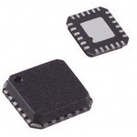
| 封装/外壳 | 24-VFQFN 裸露焊盘,CSP |
| 本底噪声 | -149dBm/Hz |
| 标准包装 | 1 |
| 测试频率 | 880MHz |
| 电压-电源 | 4.75 V ~ 5.25 V |
| 电流-电源 | 150mA |
| 视频文件 | http://www.digikey.cn/classic/video.aspx?PlayerID=1364138032001&width=640&height=505&videoID=2245193150001 |
| 输出功率 | - |


- 商务部:美国ITC正式对集成电路等产品启动337调查
- 曝三星4nm工艺存在良率问题 高通将骁龙8 Gen1或转产台积电
- 太阳诱电将投资9.5亿元在常州建新厂生产MLCC 预计2023年完工
- 英特尔发布欧洲新工厂建设计划 深化IDM 2.0 战略
- 台积电先进制程称霸业界 有大客户加持明年业绩稳了
- 达到5530亿美元!SIA预计今年全球半导体销售额将创下新高
- 英特尔拟将自动驾驶子公司Mobileye上市 估值或超500亿美元
- 三星加码芯片和SET,合并消费电子和移动部门,撤换高东真等 CEO
- 三星电子宣布重大人事变动 还合并消费电子和移动部门
- 海关总署:前11个月进口集成电路产品价值2.52万亿元 增长14.8%


PDF Datasheet 数据手册内容提取
700 MHz to 1000 MHz RF Vector Modulator Data Sheet AD8340 FEATURES FUNCTIONAL BLOCK DIAGRAM Cartesian amplitude and phase modulation VPRF QBBP QBBM VPS2 700 MHz to 1.0 GHz frequency range Continuous magnitude control of −2 dB to −32 dB 90° Continuous phase control of 0° to 360° RFIP RFOP Output third-order intercept 24 dBm RFIM RFOM Output 1 dB compression point 11 dBm 0° OAdujtupsutta nbolei sme ofldouolra −ti1o4n9 b daBnmdw/Hidz taht ufupl lt og a2i3n0 MHz CMOP IBBP IBBM DSOP 04699-001 Fast output power disable Figure 1. 4.75 V to 5.25 V single-supply voltage APPLICATIONS RF PA linearization/RF predistortion Amplitude and phase modulation Variable attenuators and phase shifters CDMA2000, GSM/EDGE linear power amplifiers Smart antennas GENERAL DESCRIPTION The AD8340 vector modulator performs arbitrary amplitude Both the RF inputs and outputs can be used differentially or and phase modulation of an RF signal. Because the RF signal single-ended and must be ac-coupled. The RF input and output path is linear, the original modulation is preserved. This part impedances are nominally 50 Ω over the operating frequency can be used as a general-purpose RF modulator, a variable range. The DSOP pin allows the output stage to be disabled attenuator/phase shifter, or a remodulator. The amplitude can quickly to protect subsequent stages from overdrive. The be controlled from a maximum of −2 dB to less than −32 dB, AD8340 operates off supply voltages from 4.75 V to 5.25 V and the phase can be shifted continuously over the entire 360° while consuming approximately 130 mA. range. For maximum gain, the AD8340 delivers an OP1dB The AD8340 is fabricated using the Analog Devices, Inc. of 11 dBm, an OIP3 of 24 dBm, and an output noise floor of proprietary, high performance 25 GHz SOI complementary −149 dBm/Hz, independent of phase. It operates over a fre- bipolar IC process. It is available in a 24-lead RoHS-compliant quency range of 700 MHz to 1.0 GHz. LFCSP package and operates over a −40°C to +85°C tempera- The baseband inputs in Cartesian I and Q format control the ture range. Evaluation boards are available. amplitude and phase modulation imposed on the RF input signal. Both I and Q inputs are dc-coupled with a ±500 mV differential full-scale range. The maximum modulation band- width is 230 MHz, which can be reduced by adding external capacitors to limit the noise bandwidth on the control lines. Rev. C Document Feedback Information furnished by Analog Devices is believed to be accurate and reliable. However, no responsibility is assumed by Analog Devices for its use, nor for any infringements of patents or other One Technology Way, P.O. Box 9106, Norwood, MA 02062-9106, U.S.A. rights of third parties that may result from its use. Specifications subject to change without notice. No license is granted by implication or otherwise under any patent or patent rights of Analog Devices. Tel: 781.329.4700 ©2004–2014 Analog Devices, Inc. All rights reserved. Trademarks and registered trademarks are the property of their respective owners. Technical Support www.analog.com
AD8340 Data Sheet TABLE OF CONTENTS Features .............................................................................................. 1 Noise and Distortion .................................................................. 11 Applications ....................................................................................... 1 Gain and Phase Accuracy .......................................................... 11 Functional Block Diagram .............................................................. 1 RF Frequency Range .................................................................. 11 General Description ......................................................................... 1 Applications Information .............................................................. 12 Revision History ............................................................................... 2 Using the AD8340 ...................................................................... 12 Specifications ..................................................................................... 3 RF Input and Matching ............................................................. 12 Absolute Maximum Ratings ............................................................ 4 RF Output and Matching .......................................................... 13 ESD Caution .................................................................................. 4 Driving the I-Q Baseband Controls ......................................... 13 Pin Configuration and Function Descriptions ............................. 5 Interfacing to High Speed DACs .............................................. 14 Typical Performance Characteristics ............................................. 6 CDMA2000 Application ........................................................... 14 Theory of Operation ...................................................................... 10 Evaluation Board ............................................................................ 16 RF Quadrature Generator ......................................................... 10 Schematic and Artwork ............................................................. 18 I-Q Attenuators and Baseband Amplifiers .............................. 11 Outline Dimensions ....................................................................... 20 Output Amplifier ........................................................................ 11 Ordering Guide .......................................................................... 20 REVISION HISTORY 3/14—Rev. B to Rev. C Added Exposed Pad Notation, Figure 2 and Table 3 ................... 5 Updated Outline Dimensions ....................................................... 20 Changes to Ordering Guide .......................................................... 20 8/07—Rev. A to Rev B Replaced Pin Configuration and Function Descriptions Section ........................................................................ 5 Changes to Figure 30 ...................................................................... 12 Changes to Figure 39 ...................................................................... 18 7/07—Rev. 0 to Rev. A Replaced Pin Configuration and Function Descriptions Section ........................................................................ 5 Changes to Ordering Guide .......................................................... 20 6/04—Revision 0: Initial Version Rev. C | Page 2 of 20
Data Sheet AD8340 SPECIFICATIONS V = 5 V, T = 25°C, Z = 50 Ω, f = 880 MHz, single-ended, ac-coupled source drive to RFIP through 5.6 nH series inductor, RFIM S A O ac-coupled through 5.6 nH series inductor to common, differential-to-single-ended conversion at output using 1:1 balun. Table 1. Parameter Conditions Min Typ Max Unit OVERALL FUNCTION Frequency Range 700 1000 MHz Maximum Gain Maximum gain setpoint for all phase setpoints −2 dB Minimum Gain V = V = 0 V −32 dB BBI BBQ Gain Control Range Relative to maximum gain 30 dB Phase Control Range Over 30 dB control range 360 Degrees Gain Flatness Over any 60 MHz bandwidth 0.25 dB Group Delay Flatness Over any 60 MHz bandwidth 10 ps RF INPUT STAGE RFIM, RFIP (Pin 21 and Pin 22) Input Return Loss From RFIP to CMRF (with 5.6 nH series inductors) 20 dB CARTESIAN CONTROL INTERFACE (I and Q) IBBP, IBBM, QBBP, QBBM (Pin 16, Pin 15, Pin 3, Pin 4) Gain Scaling 2 1/V Modulation Bandwidth 250 mV p-p sinusoidal baseband input single-ended 230 MHz Second Harmonic Distortion 250 mV p-p, 1 MHz, sinusoidal baseband input differential 47 dBc Third Harmonic Distortion 250 mV p-p, 1 MHz, sinusoidal baseband input differential 45 dBc Step Response For gain setpoint from 0.1 to 0.9 45 ns (V = 0.5 V, V = 0.55 V to 0.95 V) BBP BBM For gain setpoint from 0.9 to 0.1 47 ns (V = 0.5 V, V = 0.95 V to 0.55 V) BBP BBM RF OUTPUT STAGE RFOP, RFOM (Pin 9 and Pin 10) Output Return Loss Measured through balun 7.5 dB f = 880 MHz Gain Maximum gain setpoint −2 dB Output Noise Floor Maximum gain setpoint, no input −149 dBm/Hz P = 0 dBm, frequency offset = 20 MHz −147 dBm/Hz IN Output IP3 f1 = 880 MHz, f2 = 877.5 MHz, maximum gain setpoint 24 dBm ACPR IS-95, single carrier, P = 0 dBm, maximum gain, 62 dBc OUT phase setpoint = 45° Output 1 dB Compression Point Maximum gain 11 dBm POWER SUPPLY VPS2 (Pin 5, Pin 6, Pin 14); RFOP, RFOM (Pin 9 and Pin 10) Positive Supply Voltage 4.75 5 5.25 V Total Supply Current Includes load current 110 130 150 mA OUTPUT DISABLE DSOP (Pin 13) Disable Threshold 2.5 V Maximum Attenuation DSOP = 5 V 40 dB Enable Response Time Delay following high-to-low transition until device 15 ns meets full specifications Disable Response Time Delay following low-to-high transition until device 10 ns produces full attenuation Rev. C | Page 3 of 20
AD8340 Data Sheet ABSOLUTE MAXIMUM RATINGS Stresses above those listed under Absolute Maximum Ratings Table 2. may cause permanent damage to the device. This is a stress Parameter Rating rating only; functional operation of the device at these or any Supply Voltage VPRF, VPS2 5.5 V other conditions above those indicated in the operational DSOP 5.5 V section of this specification is not implied. Exposure to absolute IBBP, IBBM, QBBP, QBBM 2.5 V maximum rating conditions for extended periods may affect RFOP, RFOM 5.5 V device reliability. RF Input Power at Maximum Gain (50 Ω) 13 dBm (RFIP or RFIM, Single-Ended Drive) Equivalent Voltage 2.8 V p-p ESD CAUTION Internal Power Dissipation 825 mW θ (with Pad Soldered to Board) 59°C/W JA Maximum Junction Temperature 125°C Operating Temperature Range −40°C to +85°C Storage Temperature Range −65°C to +150°C Lead Temperature (Soldering, 60 sec) 300°C Rev. C | Page 4 of 20
Data Sheet AD8340 PIN CONFIGURATION AND FUNCTION DESCRIPTIONS PRF MRF FIP FIM MRF PRF V C R R C V 42 32 22 12 02 91 QFLP1 18IFLP QFLM2 17IFLM AD8340 QBBP3 16IBBP TOP VIEW QBBM4 (Not to Scale) 15IBBM VPS25 14VPS2 VPS26 13DSOP 7 8 9 01 11 21 CMOP CMOP RFOP RFOM CMOP CMOP 04699-002 NOTES 1. THE EXPOSEDPAD MUST BE CONNECTEDTO GROUND VIA A LOW IMPEDANCEPATH. Figure 2. Pin Configuration Table 3. Pin Function Descriptions Pin No. Mnemonic Description 1; 2 QFLP; QFLM Q Baseband Input Filter Pins. Connect optional capacitor to reduce Q baseband channel low-pass corner frequency. 3; 4 QBBP; QBBM Q Channel Differential Baseband Inputs. 5, 6, 14; 19, 24 VPS2; VPRF Positive Supply Voltage, 4.75 V to 5.25 V. 7, 8, 11, 12; 20, 23 CMOP; CMRF Device Common. Connect via lowest possible impedance to external circuit common. 9; 10 RFOP; RFOM Differential RF Outputs. Must be ac-coupled. Differential impedance 50 Ω nominal. 13 DSOP Output Disable. Pull high to disable output stage. 15; 16 IBBM; IBBP I Channel Differential Baseband Inputs. 17; 18 IFLM; IFLP I Baseband Input Filter Pins. Connect optional capacitor to reduce I baseband channel low-pass corner frequency. 21; 22 RFIM; RFIP Differential RF Inputs. Must be ac-coupled. Differential impedance 50 Ω nominal. EPAD Exposed Pad. The exposed pad must be connected to ground via a low impedance path. Rev. C | Page 5 of 20
AD8340 Data Sheet TYPICAL PERFORMANCE CHARACTERISTICS 0 0.4 PHASE SETPOINT = 0° 0.2 –5 B) 0.0 GAIN SETPOINT = 1.0 PHASE SETPOINT = 90° d –10 R (–0.2 O RR–0.4 –15 E dB) PHASE SETPOINT = 270° CE –0.6 AIN ( –20 MAN–0.8 GAIN SETPOINT = 0.5 G OR–1.0 –25 F ON–1.2 C –30 N –1.4 AI G–1.6 GAIN SETPOINT = 0.1 ––4305 PHASE SETPOINT = 180° 04699-003 ––12..80 04699-006 0 0.1 0.2 0.3 0.4 0.5 0.6 0.7 0.8 0.9 1.0 0 45 90 135 180 225 270 315 360 GAIN SETPOINT PHASE SETPOINT (Degrees) Figure 3. Gain Magnitude vs. Gain Setpoint at Different Phase Setpoints, Figure 6. Gain Conformance Error vs. Phase Setpoint at Different Gain RF Frequency = 880 MHz Setpoints 4 360 PHASE SETPOINT = 135° 3 330 PHASE SETPOINT = 45° dB) 2 PHASE SETPOINT = 90° 300 OR ( 1 PHASE SETPOINT = 0° 270 GAIN SETPOINT = 1.0 ERR 0 es)240 MANCE ––21 PHASE SETPOINT = 315° E (Degre128100 OR PHASE SETPOINT = 270° AS150 GAIN SETPOINT = 0.1 ONF–3 PH120 GAIN SETPOINT = 0.5 N C–4 PHASE SETPOINT = 180° 90 GAI–5 60 ––76 PHASE SETPOINT = 225° 04699-004 300 04699-007 0 0.1 0.2 0.3 0.4 0.5 0.6 0.7 0.8 0.9 1.0 0 30 60 90 120 150 180 210 240 270 300 330 360 GAIN SETPOINT PHASE SETPOINT (Degrees) Figure 4. Gain Conformance Error vs. Gain Setpoint at Figure 7. Phase vs. Phase Setpoint at Different Gain Setpoints Different Phase Setpoints 0 6 –2 4 GAIN SETPOINT = 1.0 GAIN SETPOINT = 0.1 –4 2 –6 s) e –8 gre 0 e dB) –10 GAIN SETPOINT = 0.5 R (D–2 AIN ( –12 RRO–4 GAIN SETPOINT = 1.0 G –14 E E GAIN SETPOINT = 0.5 –16 AS–6 H –18 P–8 –20 ––2224 GAIN SETPOINT = 0.1 04699-005 ––1120 04699-008 0 45 90 135 180 225 270 315 360 0 45 90 135 180 225 270 315 360 PHASE SETPOINT (Degrees) PHASE SETPOINT (Degrees) Figure 5. Gain Magnitude vs. Phase Setpoint at Different Gain Setpoints Figure 8. Phase Error vs. Phase Setpoint at Different Gain Setpoints Rev. C | Page 6 of 20
Data Sheet AD8340 –142 0 –143 –144 –0.5 Hz) –145 B) OOR (dBm/ ––114467 RF PIN = +5dBmRF PIN = –5dBm ATNESS (d–1.0 L L OISE F ––114489 RF PIN = 0dBm GAIN F–1.5 N –150 –2.0 NO RF INPUT ––115521 04699-009 –2.5 04699-012 0 0.1 0.2 0.3 0.4 0.5 0.6 0.7 0.8 0.9 1.0 700 750 800 850 900 950 1000 GAIN SETPOINT FREQUENCY (MHz) Figure 9. Output Noise Floor vs. Gain, Noise in dBm/Hz, No Carrier, Figure 12. Gain Flatness vs. Frequency, Maximum Gain, Phase Setpoint = 0° With Carrier (20 MHz Offset) PIN = −5 dBm, 0 dBm, and +5 dBm 0 0 –2 GAIN SETPOINT = 1.0 m)–10 –4 dB –6 ER (–20 W–30 FUNDAMENTAL POWER, 879MHz, 881MHz –8 O B) –10 GAIN SETPOINT = 0.5 ND P–40 AIN (d –12 DEBA–50 S87E8CMOHNzD, 8B8A2MSEHBzAND HARMONIC PRODUCT, G –14 M SI–60 –16 A T–70 U ––2108 GAIN SETPOINT = 0.1 OUTP–80 T87H7IRMDH zB, A8S83EMBHAzND HARMONIC PRODUCT, ––2224 04699-010 RF –1–0900 04699-013 700 750 800 850 900 950 1000 100 200 300 400 500 600 700 800 900 1000 FREQUENCY (MHz) DIFFERENTIAL BASEBAND INPUT LEVEL (mV p-p) (I OR Q CHANNEL DRIVENAT 1MHz) Figure 10. Gain vs. Frequency at Different Gain Setpoints Figure 13. Baseband Harmonic Distortion (700 MHz to 1000 MHz), Phase Setpoint = 0° (I and Q Channel, RF Input = 0 dBm, Balun and Cable Losses of Approximately 2 dB Not Accounted for in Plot) –145 14 TEMP = +25°C TEMP = –40°C –146 12 –147 10 m/Hz)–148 Bm) 8 TEMP = +85°C OISE (dB–149 OP1dB (d 6 N –150 4 ––115521 04699-011 02 04699-014 700 750 800 850 900 950 1000 700 750 800 850 900 950 1000 RF FREQUENCY (MHz) FREQUENCY (MHz) Figure 11. Output Noise Floor vs. Frequency, Maximum Gain, Figure 14. Output 1 dB Compression Point vs. Frequency and Temperature, No RF Carrier, Phase Setpoint = 0° Maximum Gain, Phase Setpoint = 0° Rev. C | Page 7 of 20
AD8340 Data Sheet 30 30 28 TEMP = –40°C 25 GAIN SETPOINT = 1.0 26 24 20 GAIN SETPOINT = 0.5 m)22 m) P3 (dB20 TEMP = +85°C TEMP = +25°C P3 (dB 15 OI18 OI 10 16 14 GAIN SETPOINT = 0.1 5 1102 04699-015 0 04699-018 700 750 800 850 900 950 1000 0 45 90 135 180 225 270 315 360 FREQUENCY (MHz) PHASE SETPOINT (Degrees) Figure 15. Output IP3 vs. Frequency and Temperature, Maximum Gain, I Only Figure 18. Output IP3 vs. Gain and Phase Setpoints, 2.5 MHz Carrier Spacing RBW 30kHz RFATT 20dB REFLVL VBW 30kHz MIXER –10dBm 0 dBm SWT 100ms UNIT dBm 0 0 A m) –10 B d –5 UTAM SIDEBAND POWER ( –––121500 500mV p-p1 VB Bp- pIN BPBU TINPUT OUTPUT POWER (dBm)––––––234567000000 D BASEBAND HARMONIC D SIDEBAND DTHROUGH RED SIDEBAND D BASEBAND HARMONIC 1 RM OUTP –25 –80 ECON ESIRE F FEE NDESI ECON RF –30 200mV p-p BB INPUT 04699-016 –1–0900 S D R U S 04699-019 0 50 100 150 200 250 300 350 400 CENTER 880 MHz 500 kHz/DIV SPAN 5 MHz FREQUENCY (MHz) FREQUENCY (MHz) Figure 16. I/Q Modulation Bandwidth vs. Baseband Magnitude Figure 19. Single-Sideband Performance, 880 MHz, −10 dBm RF Input; 1 MHz, 500 mV p-p Differential BB Drive 90 120 60 14 12 GAIN SETPOINT = 1.0 150 30 10 8 GAIN SETPOINT = 0.5 6 180 0 m) 4 1.5GHz B 500MHz d 2 B ( 1.5GHz 1d 0 210 330 P O –2 500MHz –4 –6 GAIN SETPOINT = 0.1 240 300 –8 ––1102 0 45 90 P1H35ASE S1E8T0POIN2T2 5(Degr2e7e0s) 315 36004699-017 ISSM11P11 ERRDFFA PPNOOCRRETT C 2WWI7R0IICTTHHLE O5U.6Tn HIN IDNUDCUTCOTROSRS 04699-020 Figure 17. Output 1dB Compression Point vs. Gain and Phase Setpoints Figure 20. Input and Output Impedance Smith Chart (with Frequency Markers) Rev. C | Page 8 of 20
Data Sheet AD8340 90 120 60 0 150 1.5GHz 500MHz 30 –5 –10 m) 180 0 dB–15 500MHz R( 1.5GHz E–20 W O 210 330 T P–25 U P–30 T U F O–35 240 300 R –40 ISSM2DP2D EP2D2OA PRNOTC RWET IC TDIH2RIF7 C1F0LTEEOR E1N TTRIAALNSFORMER 04699-021 ––54050 0.5 1.0 1.5 DS2O.0P VO2.L5TAG3E.0 (V) 3.5 4.0 4.5 5.004699-024 Figure 21. Output Impedance Smith Chart (with Frequency Markers) Figure 24. Power Shutdown Attenuation TEK FASTACQ SAMPLE 6 4 PHASE SETPOINT = 45° 2 2V/DIV s) PHASE SETPOINT = 0° Degree –20 A3 (V) R ( CH 200mV/DIV DSOP O –4 1/ R A R H E E –6 C 3 S HA –8 P PHASE SETPOINT = 90° –––111024 04699-022 CH1 200mRFV ΩOUTPUTM 10.0ns 5.0GS/s ET 200ps/pt 74.0ns 04699-025 0 0.1 0.2 0.3 0.4 0.5 0.6 0.7 0.8 0.9 1.0 CH3 2.0V A CH2 160mV GAIN SETPOINT TIME (10ns/DIV) Figure 22. Phase Error vs. Gain Setpoint by Phase Setpoint, Figure 25. Power Shutdown Response Time 5 V DC, 25°C, 880 MHz 135 134 133 mA)132 T ( 5.25V N131 E R UR130 C LY 129 5V P P U128 S 127 112265 4.75V 04699-023 –40 –30 –20 –10 0 10 20 30 40 50 60 70 80 TEMPERATURE (°C) Figure 23. Supply Current vs. Temperature Rev. C | Page 9 of 20
AD8340 Data Sheet THEORY OF OPERATION The AD8340 is a linear RF vector modulator with Cartesian Pure amplitude modulation is represented by radial movement baseband controls. In the simplified block diagram shown in of the gain vector tip at a fixed angle, while pure phase modula- Figure 26, the RF signal propagates from the left to the right tion is represented by rotation of the tip around the circle at a while baseband controls are placed above and below. The RF fixed radius. Unlike traditional I-Q modulators, the AD8340 is input is first split into in-phase (I) and quadrature (Q) compo- designed to have a linear RF signal path from input to output. nents. The variable attenuators independently scale the I and Q Traditional I-Q modulators provide a limited LO carrier path components of the RF input. The attenuator outputs are then through which any amplitude information is removed. summed and buffered to the output. VBBI I CHANNEL INPUT By controlling the relative amounts of I and Q components that LINEAR are summed, the AD8340 allows continuous magnitude and ATTENUATOR phase control of the gain. Consider the vector gain representa- V-I tion of the AD8340 expressed in polar form in Figure 27. The SINGLE-ENDED OR SINGLE-ENDED OR attenuation factors for the I and Q signal components are DIFFERENTIAL 0°/90° I-V DIFFERENTIAL 50Ω INPUT Z 50Ω OUTPUT represented on the x- and y-axis, respectively, by the baseband V-I inputs, VBBI and VBBQ. The resultant vector sum represents the LINEAR DOIUSTAPBULTE ATTENUATOR vector gain, which can also be expressed as a magnitude and panhya svee. cBtoyr a gpapilny iwngit hdiinff ethreen ut nciotm cibrcinlea tciaonn sb oe fp broasgerbaamnmd eindp. uts, Q CHANNEL INPUT VBBQ 04699-026 Figure 26. Simplified Architecture of the AD8340 A change in sign of V or V can be viewed as a change BBI BBQ Vq in sign of the gain or as a 180° phase change. The outermost +0.5 circle represents the maximum gain magnitude of unity. The MAX GAIN = 0dB circle origin implies, in theory, a gain of 0. In practice, circuit mismatches and unavoidable signal feedthrough limit the A minimum gain to approximately −40 dB. The phase angle |A| between the resultant gain vector and the positive x-axis is θ Vi –0.5 +0.5 defined as the phase shift. Note that there is a nominal, systematic insertion phase through the AD8340 to which the phase shift is added. In the following discussions, the systematic insertion phase is normalized to 0°. MIN GAIN < –30dB The correspondence between the desired gain and phase –0.5 04699-027 setpoints, GainSP and PhaseSP, and the Cartesian inputs, VBBI Figure 27. Vector Gain Representation and V , is given by simple trigonometric identities. BBQ RF QUADRATURE GENERATOR Gain = (V /V )2 +(V /V )2 The RF input is directly coupled differentially or single-endedly SP BBI O BBQ O ( ) to the quadrature generator, which consists of a multistage RC Phase =arctanV /V SP BBQ BBI polyphase network tuned over the operating frequency range of where: 700 MHz to 1000 MHz. The recycling nature of the polyphase V is the baseband scaling constant (500 mV). network generates two replicas of the input signal, which are O V and V are the differential I and Q baseband voltages, in precise quadrature, that is, 90°, to each other. Because the BBI BBQ respectively. passive network is perfectly linear, the amplitude and phase information contained in the RF input is transmitted faithfully Note that when evaluating the arctangent function, the proper to both channels. The quadrature outputs are then separately phase quadrant must be selected. For example, if the principal buffered to drive the respective attenuators. The characteristic value of the arctangent (known as the arctangent(x)) is used, impedance of the polyphase network is used to set the input Quadrant 2 and Quadrant 3 would be interpreted mistakenly impedance to the AD8340. as Quadrant 4 and Quadrant 1, respectively. In general, both V and V are needed in concert to modulate the gain and BBI BBQ the phase. Rev. C | Page 10 of 20
Data Sheet AD8340 I-Q ATTENUATORS AND BASEBAND AMPLIFIERS GAIN AND PHASE ACCURACY The proprietary linear-responding attenuator structure is an There are numerous ways to express the accuracy of the AD8340. active solution with differential inputs and outputs that offer Ideally, the gain and phase should precisely follow the setpoints. excellent linearity, low noise, and greater immunity from mis- Figure 4 illustrates the gain error in decibels (dB) from a best fit matches than other variable attenuator methods. The gain, in line, normalized to the gain measured at the gain setpoint = 1.0, linear terms, of the I and Q channels is proportional to its control for the different phase setpoints. Figure 6 shows the gain error voltage with a scaling factor designed to be 2/V, that is, a full-scale in a different form; the phase setpoint is swept from 0° to 360° gain setpoint of 1.0 (−2 dB) for V of 500 mV. The control for different gain setpoints. Figure 8 and Figure 22 show analo- BBI (Q) voltages can be driven differentially or single-endedly. The gous errors for the phase error as a function of gain and phase combination of the baseband amplifiers and attenuators allows setpoints. The accuracy clearly depends on the region of operation for maximum modulation bandwidths in excess of 200 MHz. within the vector gain unit circle. Operation very close to the OUTPUT AMPLIFIER origin generally results in larger errors as the relative accuracy of the I and Q vectors degrades. The output amplifier accepts the sum of the attenuator outputs RF FREQUENCY RANGE and delivers a differential output signal into the external load. The output pins must be pulled up to an external supply, The frequency range on the RF input is limited by the internal preferably through RF chokes. When the 50 Ω load is taken polyphase quadrature phase-splitter. The phase-splitter splits differentially, an OP1dB of 11 dBm and OIP3 of 24 dBm are the incoming RF input into two signals, 90° out of phase, as achieved at 880 MHz. The output can be taken in single-ended previously described in the RF Quadrature Generator section. fashion, albeit at lower performance levels. This polyphase network has been designed to ensure robust NOISE AND DISTORTION quadrature accuracy over standard fabrication process parameter variations for the 700 MHz to 1 GHz specified RF The output noise floor and distortion levels vary with the gain frequency range. Using the AD8340 as a single-sideband magnitude but do not vary significantly with the phase. At the modulator and measuring the resulting sideband suppression is higher gain magnitude setpoints, the OIP3 and the noise floor a good gauge of how the quadrature accuracy is maintained vary in direct proportion with the gain. At lower gain magni- over RF frequency. A typical plot of sideband suppression from tude setpoints, the noise floor levels off while the OIP3 continues 500 MHz to 1.5 GHz is shown in Figure 28. The level of sideband to vary with the gain. suppression degradation outside the 700 MHz to 1 GHz specified range is subject to manufacturing process variations. 0 –5 Bc)–10 d N ( O–15 SI S E R P–20 P U S SB –25 –30 –35 04699-028 500 600 700 800 900 1000 1100 1200 1300 1400 1500 FREQUENCY (MHz) Figure 28. Sideband Suppression vs. Frequency Rev. C | Page 11 of 20
AD8340 Data Sheet APPLICATIONS INFORMATION USING THE AD8340 RFIM, a 50 Ω match is achieved with a return loss of >10 dB over the operating frequency range. Different matching The AD8340 is designed to operate in a 50 Ω impedance inductors can improve matching over a narrower frequency system. Figure 30 illustrates where the RF input is driven in range. The single-ended and differential input impedances are a single-ended fashion while the differential RF output is exactly the same. converted to a single-ended output with an RF balun. The baseband controls for the I and Q channels are typically driven 100pF 5.6nH RFIM from differential DAC outputs. The power supplies, VPRF and RC VPS2, should be bypassed appropriately with 0.1 µF and 100 pF ~1VDC PHASE 100pF 5.6nH capacitors. Low inductance grounding of the CMOP and CMRF RF common pins is essential to prevent unintentional peaking of 50Ω RFIP 04699-029 the gain. Figure 29. RF Input Interface to the AD8340 Showing RF INPUT AND MATCHING Coupling Capacitors and Matching Inductors The RFIP and RFIM should be ac-coupled through low loss The input impedance of the AD8340 is defined by the characteris- series capacitors as shown in Figure 29. The internal dc levels tics of the polyphase network. The capacitive component of the are at approximately 1 V. For single-ended operation, one input network causes its impedance to roll off with frequency, albeit at is driven by the RF signal and the other input is ac grounded. a slower rate than 6 dB/octave. With matching inductors on the order of 5.6 nH in series with each of the RF inputs, RFIP and VP C2 C1 100pF 0.1µF IBBM VP IBBP C12 (SEE TEXT) A OUTPUT DISABLE B C8 C7 VP 0.1µF 100pF VPIFRLFP IFLM IBBP IBBM VPS2 DCSMOOPP C6 L3 CMRF CMOP C17 100pF 5.6nH 100pF ETC1-1-13 RF RFIM RFOM OUTPUT AD8340 RF RFIP RFOP INPUT C5 L4 C18 100pF 5.6nH CMRF CMOP L1 L2 100pF 120nH 120nH VP C3 C4 VPQRFFLP QFLM QBBP QBBM VPS2 VCPMSO2P C14 0.1µF 100pF 0.1µF VP C11 C10 (SEE TEXT) 0.1µF QQBBBBMP C1090pF 04699-0-030 Figure 30. Basic Connections Rev. C | Page 12 of 20
Data Sheet AD8340 RF OUTPUT AND MATCHING The RF output signal can be disabled by raising the DSOP pin to the positive supply. The shutdown function provides >40 dB The RF outputs of the AD8340, RFOP, and RFOM, are open attenuation of the input signal even at full gain. The interface collectors of a transimpedance amplifier that needs to be pulled to DSOP is high impedance, and the shutdown and turn-on up to the positive supply, preferably with RF chokes, as shown response times are <100 ns. If the disable function is not in Figure 31. The nominal output impedance looking into each needed, the DSOP should be tied to ground. individual output pin is 25 Ω. Consequently, the differential output impedance is 50 Ω. DRIVING THE I-Q BASEBAND CONTROLS VP The I and Q inputs to the AD8340 set the gain and phase between input and output. These inputs are differential and should normally have a common-mode level of 0.5 V. However, RT 120nH when differentially driven, the common mode can vary from 100pF RFOM 250 mV to 750 mV while still allowing full gain control. Each 1:1 RF ±ISIG GM 100pF OUTPUT input pair has a nominal input swing of ±0.5 V differential around the common-mode level. The maximum gain of unity RFOP RT DIFFE5R0ΩENTIAL 04699-031 i−s5 a0c0h imevVe.d T ihf etrheef odrieff, ewreitnht iaa lc voomltmagoen i-sm eqoudael lteov e+l 5o0f0 5 m00V m oVr, Figure 31. RF Output Interface to the AD8340 Showing IBBP and IBBM each swings between 250 mV and 750 mV. Coupling Capacitors, Pull-Up RF Chokes, and Balun The I and Q inputs can also be driven with a single-ended Because the output dc levels are at the positive supply, ac signal. In this case, one side of each input should be tied to a coupling capacitors are usually needed between the AD8340 low noise 0.5 V voltage source (a 0.1 µF decoupling capacitor outputs and the next stage in the system. located close to the pin is recommended), while the other input A 1:1 RF broadband output balun, such as the ETC1-1-13 swings from 0 V to 1 V. Differential drive generally offers (M/A-COM), converts the differential output of the AD8340 superior even-order distortion and lower noise than single- into a single-ended signal. Note that the loss and balance of the ended drive. balun directly impact the apparent output power, noise floor, The bandwidth of the baseband controls exceeds 200 MHz even and gain/phase errors of the AD8340. In critical applications, at full-scale baseband drive. This allows for very fast gain and narrow-band baluns with low loss and superior balance are phase modulation of the RF input signal. In cases where lower recommended. modulation bandwidths are acceptable or desired, external filter If the output is taken in a single-ended fashion directly into a capacitors can be connected across Pin IFLP to Pin IFLM, and 50 Ω load through a coupling capacitor, there is an impedance across Pin QFLP to Pin QFLM, to reduce the ingress of base- mismatch. This can be resolved with a 1:2 balun to convert the band noise and spurious signal into the control path. single-ended 25 Ω output impedance to 50 Ω. If loss-of-signal The 3 dB bandwidth is set by choosing C according to the FLT swing is not critical, a 25 Ω back termination in series with the following equation: output pin can also be used. The unused output pin must still be 45kHz×10nF pulled up to the positive supply. The user can load it through a f ≈ coupling capacitor with a dummy load to preserve balance. The 3dB C +0.5pF EXTERNAL gain of the AD8340 when the output is single-ended varies This equation has been verified for values of C from 10 pF to FLT slightly with the dummy load value, as shown in Figure 32. 0.1 µF (bandwidth settings of approximately 4.5 kHz to 43 MHz). –0.5 –1.0 RL2 = SHORT –1.5 –2.0 –2.5 B) d –3.0 N ( RL2 = 50Ω AI –3.5 G –4.0 –4.5 –5.0 ––56..50 RL2 = OPEN 04699-032 700 800 900 1000 FREQUENCY (MHz) Figure 32. Gain of the AD8340 Using a Single-Ended Output with Different Dummy Loads, RL2 on the Unused Output Rev. C | Page 13 of 20
AD8340 Data Sheet INTERFACING TO HIGH SPEED DACs 1.15 3) 1.13 The AD977x family of dual DACs is well suited for driving the G (R 11..0180 I and Q vector controls of the AD8340. While these inputs can WIN 1.05 S 1.02 in general be driven by any DAC, the differential outputs and AK 1.00 bias level of the Analog Devices TxDAC® family allow for a PE 0.97 O- 0.95 direct connection between DAC and modulator. K-T 0.92 A 0.90 The AD977x family of dual DACs has differential current E P 0.88 outputs. The full-scale current is user programmable and is AL 0.85 usually set to 20 mA, that is, each output swings from 0 mA RENTI 00..8802 to 20 mA. FE 0.77 The basic interface between the AD9777 DAC outputs and the DIF 000...777052 04699-034 AD8340 I and Q inputs is shown in Figure 33. The resistors R1 50 55 60 65 70 75 80 85 90 95 100105110115120125130 and R2 set the dc bias level according to the equation: R3 Figure 34. Peak-to-Peak DAC Output Swing vs. Bias Level = Average Output Current × R1 Swing Scaling Resistor R3 (R1 = R2 = 50 Ω) For example, if the full-scale current from each output is 20 mA, Figure 34 shows the relationship between the value of R3 and each output will have an average current of 10 mA. Therefore, the peak baseband voltage with R1 and R2 equal to 50 Ω. Figure 34 to set the bias level to the recommended 0.5 V, R1 and R2 shows that a value of 100 Ω for R3 provides a peak-to-peak should be set to 50 Ω each. R1 and R2 should always be equal. swing of 1 V p-p differential into the AD8340 I and Q inputs. If R3 is omitted, this results in an available swing from the DAC When using a DAC, low-pass image reject filters are typically of 2 V p-p differential, which is twice the maximum voltage used to eliminate the Nyquist images produced by the DAC. range required by the AD8340. DAC resolution can be They also provide the added benefit of eliminating broadband maximized by adding R3, which scales down this voltage noise that might feed into the modulator from the DAC. according to the following equation: CDMA2000 APPLICATION Full−ScaleSwing = To test the compliance to the CDMA2000 base station standard, ( ) R2 2×I R1 (R2+R3) ×1− a single-carrier CDMA2000 test model signal (forward pilot, sync, MAX R2+R3 paging, and six traffic as per 3GPP2 C.S0010-B, Table 6.5.2.1) was applied to the AD8340. A cavity-tuned filter was used to AD9777 AD8340 reduce noise from the signal source being applied to the device. The 4.6 MHz pass band of this filter is apparent in the IOUTA1 IBBP R1 OPTIONAL subsequent spectral plots (see Figure 35 to Figure 38). LOW-PASS FILTER R3 R2 Figure 35 shows a plot of the spectrum of the output signal IOUTB1 IBBM under nominal conditions. P is equal to −5 dBm and V = V OUT I Q = 0.353 V, that is, VIBBP − VIBBM = VQBBP − VQBBM = 0.353 V. Adjacent channel power is measured in 30 kHz IOUTA2 QBBP resolution bandwidth at 750 kHz and 1.98 MHz carrier offset. R1 OPTIONAL LOW-PASS R3 Noise floor is measured at ±4 MHz carrier offset. R2 FILTER IOUTB2 QBBM 04699-033 Figure 33. Basic AD9777 to AD8340 Interface Rev. C | Page 14 of 20
Data Sheet AD8340 BS, 1X, C0 :ADJ CHANNEL *RBW 30kHz MARKER 2 [T1 NOI] 10 –50 W) *VBW 30kHz –148.76dBm/Hz B REF O–1F2FdSBEmT 0.5 dB *ATT 5dB *SWT 100msCH P 8W7R6.009–651.51378d5BMmHz 0 POUT vs. VIN –55 MHz R –20 ACP LOW –60.94dB 1 –––––4563700000 SWP 50 OF 50 AAAM CLL TTPA 8 118 RU 4UL K P.O–P0E10WR46 841.1––– 8[06889T2066d15...B 048N6800mMOddd/HBBBIH]zz LNVOLR OUTPUT POWER (dBm)––––12340000 ACP – 1A.C98PM –H 7z5 O0kFHFzS OETF,F 3S0EkHT,z 3 R0kBHWz RBW ––––66770505 ACP – dBc (30kHz RBW)CARRIER OFFSET – dBm ( –80 –50 –80 Hz M –––11910000 2 1 04699-035 ––67000 50 1N0O0ISE1 –5 04MHV2zI0 =0O VFQF2S=5EV0TIN, 1(3mM0VH0)z R3B5W0 400 450 500––8950 NOISE – 404699-037 CENTER 880MHz 1MHz/DIV SPAN 10MHz Figure 37. Output Power, Noise, and ACP vs. I and Q Control Voltages, Figure 35. Output Spectrum, Single-Carrier CDMA2000 Test Model at −5 dBm VI = VQ = 0.353 V, ACP Measured at 750 kHz and 1.98 MHz Carrier Offset, CaDnMdA ±210.0908 TMeHstz M Caordreiel,r V OI =ffs VeQt,, NACoPis eM Meaesausruerde din a 3t 0± k4H Mz HRzB WCa arrti e±r7 O5f0f skeHt z Noise Measured at ±4 MHz Carrier Offset, Input Signal Filtered Using a Cavity Tuned Filter (Pass Band = 4.6 MHz) In contrast to Figure 36, Figure 37 shows that for a fixed input Holding the I and Q control voltages steady at 0.353 V, input power, ACP remains fairly constant as gain and phase are power was swept. Figure 36 shows the resulting output power, changed (this is not true for very high input powers). The noise noise floor, and adjacent channel power ratio. Noise floor is floor still drops with decreasing gain, but it never reaches the presented as noise in a 1 MHz bandwidth as defined by the −90 dBm level shown in Figure 37. 3GPP2 specification. Figure 38 shows the output spectrum for a 3-carrier CDMA2000 –30 –30 W) spectrum. Again, the signal being applied to the AD8340 is B –40 –40 MHz R f4i.l6te MreHd zb.y T ao c raevdituyc-et udnisetdo rftiiltoenr, wthiteh t oa t−al3 o duBtp buatn cdawrriidetrh p oofw er 1 W) –50 –50 SET ( was reduced to approximately −8 dBm (per-carrier power = kHz RB –60 –60 ER OFF −fr1o2m.6 c deBntmer) .o Af dspjaeccetnrut mch)a annnde l− p8o2w deBr cr a(t3i.o2s3 o Mf −H6z1 f droBmc (c2e MnteHr z P – dBc (30 –70 ACP – 750kHz OFFSET, 30kHz RBW –70 MHz CARRI o5in.f2 sa5p 1Me cMHtrHzu mcza b)r rawineerdr woef ifmdsetehta, )si.su Warpehdpi.rl oTex hsiomem natoee ildsyey − nf1lao4mo9r id,c B mrmaena/gHseuz ri se( −dlo8 as9tt d dBume AC –80 ACP – 1.98MHz OFFSET, 30kHz RBW –80 @ 4 to output power back-off, ACP stays approximately equal and m –90 –90 dB noise floor improves slightly. –100 NOISE – 4MHz OFFSET, 1MHz RBW –100OISE – 04699-036 **RVBBWW 33000kkHHzz M A R K –E1R4 81. 8[3Td1B NmO/IH]z –30 –25 –20 –15 –10 –5 0 5 N REF –15 dBm *ATT 5dB *SWT 5s 885.252403846MHz OUTPUT POWER (dBm) –20 OFFSET 0.5dB CCHH12 ––1122..6585ddBBm Figure 36. Noise and ACP vs. Output Power, –30 CTOHT3AL ––712.9.837ddBB SAOL Single-Carrier CDMA2000 Test Model, VI = VQ = 0.353, ACP LOW –61.41dB ACP Measured in 30 kHz RBW at ±750 kHz and ±1.98 MHz Carrier Offset, –40 ACP UP –61.87dB LVL ALT1 LOW –82.36dB Noise Measured at ±4 MHz Carrier Offset –50 ALT1 UP –81.92dB NOR The results show that at an output power of 3 dBm, ACP is still –60 in compliance with the standard (<−45 dBc at 750 MHz and –70 <−60 dBc at 1.98 MHz). At low output power levels, ACP at –80 1.98 MHz, carrier offset degrades as the noise floor of the AD8340 becomes the dominant contributor to measured ACP. –90 Mshaerapsluyr aebdo nveo i0s ed Batm 4 o MutHpuzt cpaorwrieerr. Tohffisse itn bcreegaisnes i sto n oint cdrueea stoe noise. ––110100 1 04699-038 but results from increased carrier-induced distortion. As output CENTER 880MHz 1.5MHz/ SPAN 15MHz power drops below 0 dBm, the noise floor drops towards −90 dBm. Figure 38. Output Spectrum, 3-Carrier CDMA2000 Test Model at −12.5 dBm/Carrier, VI = VQ = 0.353 V, ACP Measured at 2 MHz and 3.23 kHz With a fixed input power of 2.4 dBm, the output power was Offset from Center of Spectrum, Noise Measured at 5.25 MHz Carrier Offset, again swept by exercising the I and Q inputs. V and V were Input Signal Filtered Using a Cavity-Tuned Filter (Pass Band = 4.6 MHz) I Q kept equal and were swept from 10 mV to 500 mV. The resulting output power, ACP, and noise floor are shown in Figure 37. Rev. C | Page 15 of 20
AD8340 Data Sheet EVALUATION BOARD The baseband input of the AD8340 requires a differential The evaluation board circuit schematic for the AD8340 is voltage drive. The evaluation board is set up to allow such a shown in Figure 39. drive by connecting the differential voltage source to QBBP and The evaluation board is configured to be driven from a QBBM. The common-mode voltage should be maintained at single-ended 50 Ω source. Although the input of the AD8340 approximately 0.5 V. For this configuration, Jumper W1 to is differential, it may be driven single-ended with no loss of Jumper W4 should be removed. performance. The baseband input of the evaluation board can also be driven The low-pass corner frequency of the baseband I and Q with a single-ended voltage. In this case, a bias level is provided channels can be reduced by installing capacitors in the C11 and to the unused input from Potentiometer R10 by installing either C12 positions. The low-pass corner frequency for either W1 or W2. channel is approximated by Setting SW1 in Position B disables the AD8340 output 45kHz×10nF f ≈ amplifier. With SW1 set to Position A, the output amplifier is 3dB C +0.5pF enabled and an external voltage signal, such as a pulse, can be EXTERNAL applied to the DSOP SMA connector to exercise the output On the evaluation board, the I and Q baseband circuits are amplifier enable/disable function. identical, so the following description applies equally to each. The connections and circuit configuration for the Q baseband inputs are described in Table 4. Rev. C | Page 16 of 20
Data Sheet AD8340 Table 4. Evaluation Board Configuration Options Components Description Default Conditions R7, R9, R11, R14, I Channel Baseband Interface. Resistor R7 and Resistor R9 can be R7, R9 = open R15, R19, R20, R21, installed to accommodate a baseband source that requires a R11 = potentiometer, 2 kΩ, 10 turns (Bourns) C15, C19, W3, W4 specific terminating impedance. C15 and C19 are bypass R14 = 4 kΩ (Size 0603) capacitors. For single-ended baseband drive, Potentiometer R11 R15 = 44 kΩ (Size 0603) can be used to provide a bias level to the unused input (install R19, R20, R21 = 0 Ω (Size 0603) either W3 or W4). C15, C19 = 0.1 µF (Size 0603) W3 = jumper (installed) W4 = jumper (open) R1, R3, R10, R12, Q Channel Baseband Interface. See the I Channel Baseband R1, R3 = open R13, R16, R17, R18, Interface description. R10 = potentiometer, 2 kΩ, 10 turns (Bourns) C16, C20, W1, W2 R12 = 4 kΩ (Size 0603) R13 = 44 kΩ (Size 0603) R16, R17, R18 = 0 Ω (Size 0603) C16, C20 = 0.1 µF (Size 0603) W1 = jumper (installed) W2 = jumper (open) C11, C12 Baseband Low-Pass Filtering. By adding Capacitor C11 between C11, C12 = open QFLP and QFLM, and Capacitor C12 between IFLP and IFLM, the 3 dB low-pass corner frequency of the baseband interface can be reduced from 230 MHz (nominal). See the equation in the Evaluation Board section. T1, C17, C18, L1, L2 Output Interface. The 1:1 balun transformer, T1, converts the 50 Ω C17, C18 = 100 pF (Size 0603) differential output to 50 Ω single-ended. C17 and C18 are dc T1 = ETC1-1-13 (M/A-COM) blocks. L1 and L2 provide dc bias for the output. L1, L2 = 120 nH (Size 0603) L3, L4, C5, C6 Input Interface. The input impedance of the AD8340 requires 5.6 nH L3, L4 = 5.6 nH (Size 0402) inductors in series with RFIP and RFIM for optimum return loss C5, C6 = 100 pF (Size 0603) when driven by a single-ended 50 Ω line. C5 and C6 are dc blocks. C2, C4, C7, C9, C14, Supply Decoupling. C2, C4, C7, C9 = open (Size 0603) C1, C3, C8, C10, C1, C3, C8, C10, C14 = 0.1 µF (Size 0603) R2, R4, R5, R6 R2, R4, R5, R6 = 0 Ω (Size 0603) R8, SW1 Output Disable Interface. The output stage of the AD8340 is R8 = 10 kΩ (Size 0603) disabled by applying a high voltage to the DSOP pin by moving SW1 = SPDT (Position A, output enabled) SW1 to Position B. The output stage is enabled by moving SW1 to Position A. The output disable function can also be exercised by applying an external high or low voltage to the DSOP SMA connector with SW1 in Position A. Rev. C | Page 17 of 20
AD8340 Data Sheet SCHEMATIC AND ARTWORK IBBP IBBM R9 C19 R7 (OPEN) 0.1µF(OPEN) VP GND TEST POINT TEST POINT R19 0Ω W4 W3 C2 R21 C15 R20 (OPEN) 0Ω 0.1µF 0Ω R2 VS 0Ω R14 R11 R15 4kΩ 2kΩ 44kΩ C1 0.1µF C12 (OPEN) SW1 B R8 A VP C(O7PEN) 0RΩ5 C0.81µF VPIFRLFP IFLM IBBP IBBM VPS2 DCSMOOPP 10kΩ DSOP T1 C6 L3 CMRF CMOP C17 ETC1-1-13 100pF 5.6nH 100pF M/A-COM RFIM RFOM RFOP AD8340 RFIN RFIP RFOP C5 L4 C18 100pF 5.6nH CMRF CMOP L1 L2 100pF 120nH 120nH VP C4 R4 C3 VQPRFLFP QFLM QBBP QBBM VPS2 VCPMSO2P C14 (OPEN) 0Ω 0.1µF 0.1µF VP C11 C10 R6 C9 (OPEN) 0.1µF 0Ω (OPEN) R12 R10 R13 4kΩ 2kΩ 44kΩ VS C16 0.1µF W2 W1 R17 R18 R16 0Ω 0Ω 0Ω R1 R3 OPEN C20 OPEN 0.1µF QBBP QBBM 04699-039 Figure 39. Evaluation Board Schematic Rev. C | Page 18 of 20
Data Sheet AD8340 04699-040 04699-0-041 Figure 40. Component Side Layout Figure 41. Component Side Silkscreen Rev. C | Page 19 of 20
AD8340 Data Sheet OUTLINE DIMENSIONS 4.10 0.30 4.00 SQ 0.25 PIN 1 3.90 0.20 INDICATOR PIN 1 0.50 19 24 INDICATOR BSC 18 1 EXPOSED 2.20 PAD 2.10 SQ 2.00 13 6 0.50 12 7 0.25 MIN TOP VIEW 0.40 BOTTOM VIEW 0.30 FOR PROPER CONNECTION OF 0.80 THE EXPOSED PAD, REFER TO 0.75 0.05 MAX THE PIN CONFIGURATION AND 0.70 0.02 NOM FUNCTION DESCRIPTIONS SECTION OF THIS DATA SHEET. COPLANARITY SEATING 0.08 PLANE COMPLIANTTOJED0E.2C0 SRTEAFNDARDS MO-220-WGGD-8. 06-11-2012-A Figure 42. 24-Lead Lead Frame Chip Scale Package [LFCSP_WQ] 4 mm × 4 mm Body, Very Very Thin Quad (CP-24-10) Dimensions shown in millimeters ORDERING GUIDE Package Ordering Model1, 2 Temperature Range Package Description Option Quantity AD8340ACPZ-WP −40°C to +85°C 24-Lead Lead Frame Chip Scale Package [LFCSP_WQ] CP-24-10 64 AD8340ACPZ-REEL7 −40°C to +85°C 24-Lead Lead Frame Chip Scale Package [LFCSP_WQ] CP-24-10 1,500 AD8340-EVALZ Evaluation Board 1 1 Z = RoHS Compliant Part. 2 WP = Waffle pack. ©2004–2014 Analog Devices, Inc. All rights reserved. Trademarks and registered trademarks are the property of their respective owners. D04699-0-3/14(C) Rev. C | Page 20 of 20