ICGOO在线商城 > 射频/IF 和 RFID > RF 调制器 > ADRF6750ACPZ-R7

 Datasheet下载
- 型号: ADRF6750ACPZ-R7
- 制造商: Analog
- 库位|库存: xxxx|xxxx
- 要求:
| 数量阶梯 | 香港交货 | 国内含税 |
| +xxxx | $xxxx | ¥xxxx |
查看当月历史价格
查看今年历史价格
ADRF6750ACPZ-R7产品简介:
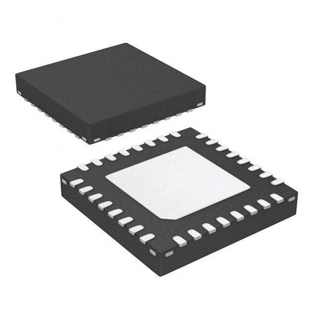
ICGOO电子元器件商城为您提供ADRF6750ACPZ-R7由Analog设计生产,在icgoo商城现货销售,并且可以通过原厂、代理商等渠道进行代购。 ADRF6750ACPZ-R7价格参考¥78.38-¥109.31。AnalogADRF6750ACPZ-R7封装/规格:RF 调制器, RF Modulator IC 950MHz ~ 1.575GHz 56-VFQFN 裸露焊盘,CSP。您可以下载ADRF6750ACPZ-R7参考资料、Datasheet数据手册功能说明书,资料中有ADRF6750ACPZ-R7 详细功能的应用电路图电压和使用方法及教程。
ADRF6750ACPZ-R7是Analog Devices Inc.推出的一款高性能直接上变频调制器,主要应用于射频(RF)信号处理领域。该器件集成了I/Q混频器、可变增益放大器(VGA)、正交相位发生器和小数N分频锁相环(PLL)及压控振荡器(VCO),支持宽频带输出(约1500 MHz至2700 MHz),适用于无线通信系统中的关键射频模块。

典型应用场景包括:4G LTE和5G无线基站的发射链路设计,尤其是微蜂窝、微微基站和远程射频单元(RRU);工业与通信领域的宽带无线回传系统;软件定义无线电(SDR)平台,因其高集成度和灵活调谐能力,有助于简化射频设计并减少外围元件数量;还可用于测试测量设备、专用无线网络以及需要高性能调制功能的射频发射系统。

ADRF6750ACPZ-R7支持I/Q输入信号直接调制到RF频段,具备优异的边带抑制性能和低本振泄漏,有利于提升通信质量。其采用32引脚LFCSP封装,适合高密度PCB布局,并通过串行接口实现寄存器配置,便于系统集成与控制。整体方案具有高线性度、低功耗和良好的温度稳定性,满足严苛工业环境下的长期可靠运行需求。
| 参数 | 数值 |
| 产品目录 | |
| 描述 | IC QUADRATURE MODULATOR 56LFCSP |
| 产品分类 | |
| LO频率 | - |
| 品牌 | Analog Devices Inc |
| 数据手册 | |
| 产品图片 |
|
| P1dB | 8.5dBm |
| 产品型号 | ADRF6750ACPZ-R7 |
| RF频率 | 950MHz ~ 1.575GHz |
| rohs | 无铅 / 符合限制有害物质指令(RoHS)规范要求 |
| 产品系列 | - |
| 其它名称 | ADRF6750ACPZ-R7DKR |
| 功能 | 调制器 |
| 包装 | Digi-Reel® |
| 封装/外壳 | 56-VFQFN 裸露焊盘,CSP |
| 本底噪声 | -162dBm/Hz |
| 标准包装 | 1 |
| 测试频率 | - |
| 电压-电源 | 4.75 V ~ 5.25 V |
| 电流-电源 | 310mA |
| 视频文件 | http://www.digikey.cn/classic/video.aspx?PlayerID=1364138032001&width=640&height=505&videoID=2245193150001http://www.digikey.cn/classic/video.aspx?PlayerID=1364138032001&width=640&height=505&videoID= 2474683260001 |
| 输出功率 | -1.6dBm |


- 商务部:美国ITC正式对集成电路等产品启动337调查
- 曝三星4nm工艺存在良率问题 高通将骁龙8 Gen1或转产台积电
- 太阳诱电将投资9.5亿元在常州建新厂生产MLCC 预计2023年完工
- 英特尔发布欧洲新工厂建设计划 深化IDM 2.0 战略
- 台积电先进制程称霸业界 有大客户加持明年业绩稳了
- 达到5530亿美元!SIA预计今年全球半导体销售额将创下新高
- 英特尔拟将自动驾驶子公司Mobileye上市 估值或超500亿美元
- 三星加码芯片和SET,合并消费电子和移动部门,撤换高东真等 CEO
- 三星电子宣布重大人事变动 还合并消费电子和移动部门
- 海关总署:前11个月进口集成电路产品价值2.52万亿元 增长14.8%


PDF Datasheet 数据手册内容提取
950 MHz to 1575 MHz Quadrature Modulator with Integrated Fractional-N PLL and VCO ADRF6750 FEATURES GENERAL DESCRIPTION I/Q modulator with integrated fractional-N PLL and VCO The ADRF6750 is a highly integrated quadrature modulator, Gain control span: 47 dB in 1 dB steps frequency synthesizer, and programmable attenuator. The Output frequency range: 950 MHz to 1575 MHz device covers an operating frequency range from 950 MHz Output 1 dB compression: 8.5 dBm to 1575 MHz for use in satellite, cellular and broadband Output IP3: 23 dBm communications. Noise floor: −162 dBm/Hz The ADRF6750 modulator includes a high modulus fractional-N Baseband modulation bandwidth: 250 MHz (1 dB) frequency synthesizer with integrated VCO, providing better Output frequency resolution: 1 Hz than 1 Hz frequency resolution, and a 47 dB digitally controlled Functions with external VCO for extended frequency range output attenuator with 1 dB steps. SPI and I2C-compatible serial interfaces Power supply: 5 V/310 mA Control of all the on-chip registers is through a user-selected SPI interface or I2C interface. The device operates from a single power supply ranging from 4.75 V to 5.25 V. FUNCTIONAL BLOCK DIAGRAM VCC1 VCC2 VCC3 VCC4 REGOUT 3.3V REGULATOR IBBP VREG1 IBBN VREG2 VREG3 VREG4 CCOMP1 VREG5 CCOMP2 VREG6 CCOMP3 47dB LLOOMMOONNNP GAINR ACNOGNETROL 0°/90° OSUTTAPGUET VCO VTUNE CORE RFOUT TESTLO TXDIS TESTLO QBBP QBBN RSET REFERENCE REFIN DOU×B2LER DI5V-BIDITER ÷2 + PHASE REFIN –FDREETQEUCETNOCRY CHPUAMRGPE CP CURRENT SETTING LF3 N-COUNTER LF2 THIRD-ORDER LDET SDI/SDA FRACTIONAL RFCP4 RFCP3 RFCP2 RFCP1 CLK/SCL SI2PCI/ INTERPOLATOR SDO INTERFACE CS FRACTIONAL MODULUS INTEGER REGISTER 225 REGISTER ADRF6750 AGND DGND 08201-001 Figure 1. Rev. A Information furnished by Analog Devices is believed to be accurate and reliable. However, no responsibility is assumed by Analog Devices for its use, nor for any infringements of patents or other One Technology Way, P.O. Box 9106, Norwood, MA 02062-9106, U.S.A. rights of third parties that may result from its use. Specifications subject to change without notice. No license is granted by implication or otherwise under any patent or patent rights of Analog Devices. Tel: 781.329.4700 www.analog.com Trademarks and registered trademarks are the property of their respective owners. Fax: 781.461.3113 ©2010 Analog Devices, Inc. All rights reserved.
ADRF6750 TABLE OF CONTENTS Features .............................................................................................. 1 I2C Interface ................................................................................ 21 General Description ......................................................................... 1 SPI Interface ................................................................................ 23 Functional Block Diagram .............................................................. 1 Program Modes .......................................................................... 25 Revision History ............................................................................... 2 Register Map ................................................................................... 27 Specifications ..................................................................................... 3 Register Map Summary ............................................................. 27 Timing Characteristics ................................................................ 5 Register Bit Descriptions ........................................................... 28 Absolute Maximum Ratings ............................................................ 7 Suggested Power-Up Sequence ..................................................... 31 ESD Caution .................................................................................. 7 Initial Register Write Sequence ................................................ 31 Pin Configuration and Function Descriptions ............................. 8 Evaluation Board ............................................................................ 32 Typical Performance Characteristics ........................................... 10 General Description ................................................................... 32 Theory of Operation ...................................................................... 18 Hardware Description ............................................................... 32 Overview ...................................................................................... 18 PCB Artwork............................................................................... 35 PLL Synthesizer and VCO ......................................................... 18 Bill of Materials ........................................................................... 38 Quadrature Modulator .............................................................. 20 Outline Dimensions ....................................................................... 39 Attenuator .................................................................................... 21 Ordering Guide .......................................................................... 39 Voltage Regulator ....................................................................... 21 EXTERNAL vco OPERATION ................................................ 21 REVISION HISTORY 4/10—Rev. 0 to Rev. A Changes to Table 5 ............................................................................ 9 Changes to LOMON Outputs Section ......................................... 33 Changes to Ordering Guide .......................................................... 39 1/10—Revision 0: Initial Version Rev. A | Page 2 of 40
ADRF6750 SPECIFICATIONS V = 5 V, T = 25°C, I/Q inputs = 0.9 V p-p differential sine waves in quadrature on a 500 mV dc bias, baseband frequency = 1 MHz, CC A REFIN = 10 MHz, PFD = 20 MHz, loop bandwidth = 50 kHz, and LOMONx is off, unless otherwise noted. Table 1. Parameter Test Conditions/Comments Min Typ Max Unit RF OUTPUT RFOUT pin Operating Frequency Range 950 1575 MHz Nominal Output Power V = 0.9 V p-p differential −1.6 dBm IQ Gain Flatness Any 40 MHz ±0.5 dB Output P1dB 8.5 dBm Output IP3 f1 = 3.5 MHz, f2 = 4.5 MHz, P = −6 dBm per tone 23 dBm BB BB OUT Output Return Loss Attenuator setting = 0 dB −12 dB LO Carrier Feedthrough Attenuator setting = 0 dB to 47 dB −45 dBc 2× LO Carrier Feedthrough Attenuator setting = 0 dB to 47 dB −45 dBm Sideband Suppression −45 dBc Noise Floor I/Q inputs = 0 V p-p differential, Attenuator setting = 0 dB −162 dBm/Hz Attenuator setting = 0 dB to 21 dB, carrier offset = 15 MHz −147 dBc/Hz Attenuator setting = 21 dB to 47 dB, carrier offset = 15 MHz −170 dBm/Hz Harmonics −60 dBc REFERENCE CHARACTERISTICS REFIN pin Input Frequency With R/2 divider enabled 10 300 MHz With R/2 divider disabled 10 165 MHz Input Sensitivity AC-coupled 0.4 VREG V p-p Input Capacitance 10 pF Input Current ±100 μA CHARGE PUMP I Sink/Source Programmable CP High Value With RSET = 4.7 kΩ 5 mA Low Value 312.5 μA Absolute Accuracy With RSET = 4.7 kΩ 4.0 % RSET Value 4.7 kΩ VCO Gain K 25 MHz/V VCO SYNTHESIZER SPECIFICATIONS Frequency Resolution 1 Hz Spurs Integer boundary < loop bandwidth −55 dBc >10 MHz offset from carrier −85 dBc Phase Noise1 Frequency = 950 MHz to 1575 MHz 100 Hz offset −80 dBc/Hz 1 kHz offset −88 dBc/Hz 10 kHz offset −93 dBc/Hz 100 kHz offset −107 dBc/Hz 1 MHz offset −133 dBc/Hz >15 MHz offset −152 dBc/Hz Integrated Phase Noise1 1 kHz to 8 MHz integration bandwidth 0.4 °rms Frequency Settling1 Maximum frequency error = 100 Hz 170 μs Maximum Frequency Step for Frequency step with no autocalibration routine; 100 kHz No Autocalibration Register CR24, Bit 0 = 1 Phase Detector Frequency 10 30 MHz Rev. A | Page 3 of 40
ADRF6750 Parameter Test Conditions/Comments Min Typ Max Unit GAIN CONTROL Gain Range 47 dB Step Size 1 dB Relative Step Accuracy Fixed frequency, adjacent steps All attenuation steps ±0.3 dB Over full frequency range, adjacent steps ±1.5 dB Absolute Step Accuracy2 47 dB attenuation step −2.0 dB Output Settling Time Any step; output power settled to ±0.2 dB 10 μs OUTPUT DISABLE TXDIS pin Off Isolation RF OUT, attenuator setting = 0 dB to 47 dB, TXDIS high −110 dBm LO, Attenuator setting = 0 dB to 47 dB, TXDIS high −90 dBm 2 x LO, Attenuator setting = 0 dB to 47 dB, TXDIS high −50 dBm Turn-On Settling Time TXDIS high to low (90% of envelope) 180 ns Turn-Off Settling Time TXDIS low to high (to −55 dBm) 270 ns MONITOR OUTPUT LOMONP, LOMONN pins Nominal Output Power −24 dBm BASEBAND INPUTS IBBP, IBBN, QBBP, QBBN pins I and Q Input Bias Level 500 mV 1 dB Bandwidth 250 MHz LOGIC INPUTS Input High Voltage, V CS, TXDIS pins 1.4 V INH Input Low Voltage, V CS, TXDIS pins 0.6 V INL Input High Voltage, V SDI/SDA, CLK/SCL pins 2.1 V INH Input Low Voltage, V SDI/SDA, CLK/SCL pins 1.1 V INL Input Current, I /I CS, TXDIS, SDI/SDA, CLK/SCL pins ±1 μA INH INL Input Capacitance, C CS, TXDIS, SDI/SDA, CLK/SCL pins 10 pF IN LOGIC OUTPUTS Output High Voltage, V SDO, LDET pins; I = 500 μA 2.8 V OH OH Output Low Voltage, V SDO, LDET pins; I = 500 μA 0.4 V OL OL SDA (SDI/SDA); I = 3 mA 0.4 V OL POWER SUPPLIES VCC1, VCC2, VCC3, VCC4, VREG1, VREG2, VREG3, VREG4, VREG5, VREG6, and REGOUT pins REGOUT normally connected to VREG1, VREG2, VREG3, VREG4, VREG5, and VREG6 Voltage Range VCC1, VCC2, VCC3, and VCC4 4.75 5 5.25 V REGOUT, VREG1, VREG2, VREG3, VREG4, VREG5, and VREG6 3.3 V Supply Current VCC1, VCC2, VCC3, and VCC4 combined; REGOUT con- 310 340 mA nected to VREG1, VREG2, VREG3, VREG4, VREG5, and VREG6 Operating Temperature −40 +85 °C 1 LBW = 50 kHz at LO = 1200 MHz; ICP = 2.5 mA. 2 All other attenuation steps have an absolute error of <±2.0 dB. Rev. A | Page 4 of 40
ADRF6750 TIMING CHARACTERISTICS I2C Interface Timing Table 2. Parameter1 Symbol Limit Unit SCL Clock Frequency f 400 kHz max SCL SCL Pulse Width High t 600 ns min HIGH SCL Pulse Width Low t 1300 ns min LOW Start Condition Hold Time t 600 ns min HD;STA Start Condition Setup Time t 600 ns min SU;STA Data Setup Time t 100 ns min SU;DAT Data Hold Time t 300 ns min HD;DAT Stop Condition Setup Time t 600 ns min SU;STO Data Valid Time t 900 ns max VD;DAT Data Valid Acknowledge Time t 900 ns max VD;ACK Bus Free Time t 1300 ns min BUF 1 See Figure 2. t tSU;DAT tVVDD;;DAACTK A(ANCDK SIGNAL ONLY) tBUF SDA tHD;STA tSU;STA tSU;STO t LOW SCL COSNTDASIRTITON 1/tfHSDC;LDAT tHIGH S COSNTDPOITPION S 08201-003 Figure 2. I2C Port Timing Diagram Rev. A | Page 5 of 40
ADRF6750 SPI Interface Timing Table 3. Parameter1 Symbol Limit Unit CLK Frequency f 20 MHz max CLK CLK Pulse Width High t 15 ns min 1 CLK Pulse Width Low t 15 ns min 2 Start Condition Hold Time t 5 ns min 3 Data Setup Time t 10 ns min 4 Data Hold Time t 5 ns min 5 Stop Condition Setup Time t 5 ns min 6 SDO Access Time t 15 ns min 7 CS to SDO High Impedance t 25 ns max 8 1 See Figure 3. t 3 CS t 1 CLK t 6 t 2 SDI t t 4 5 SDO t7 t8 08201-004 Figure 3. SPI Port Timing Diagram Rev. A | Page 6 of 40
ADRF6750 ABSOLUTE MAXIMUM RATINGS Table 4. Stresses above those listed under Absolute Maximum Ratings Parameter Rating may cause permanent damage to the device. This is a stress Supply Voltage VCC1, VCC2, VCC3, and VCC4 −0.3 V to +6 V rating only; functional operation of the device at these or any Supply Voltage VREG1, VREG2, VREG3, VREG4, −0.3 V to +4 V other conditions above those indicated in the operational VREG5, and VREG6 section of this specification is not implied. Exposure to absolute IBBP, IBBN, QBBP, and QBBN 0 V to 2.5 V maximum rating conditions for extended periods may affect Digital I/O −0.3 V to +4 V device reliability. Analog I/O (Other Than IBBP, IBBN, QBBP, −0.3 V to +4 V and QBBN) ESD CAUTION TESTLO, TESTLO Difference 1.5 V θ (Exposed Paddle Soldered Down) 26°C/W JA Maximum Junction Temperature 120°C Storage Temperature Range −65°C to +150°C Rev. A | Page 7 of 40
ADRF6750 PIN CONFIGURATION AND FUNCTION DESCRIPTIONS T 2CCV2CCVDNGADNGADNGADNGADNGADNGATUOFRDNGADNGASIDXTTEDLUOXUM 65432109876543 55555554444444 VCC4 1 PIN 1 42VCC3 IBBP 2 INDICATOR 41VCC3 IBBN 3 40AGND QBBN 4 39AGND QBBP 5 38VTUNE AGND 6 ADRF6750 37AGND RSET 7 36VREG6 LF3 8 TOP VIEW 35CCOMP3 CP 9 (Not to Scale) 34CCOMP2 LF210 33CCOMP1 VCC111 32DGND REGOUT12 31VREG5 VREG113 30CLK/SCL VREG214 29SDI/SDA 5161718191021222324252627282 34NNDDDOODPNSO GERVGERVIFERIFERNGANGANGALTSETLTSETNGANOMOLNOMOLCDS N1 . O CATO ELNSONWE CIMTP EEXDPAONSCEED P PAATDH .TO GROUND PLANE VIA 08201-005 Figure 4. Pin Configuration Table 5. Pin Function Descriptions Pin No. Mnemonic Description 11, 55, 56, 41, 42, 1 VCC1 to VCC4 Positive Power Supplies for I/Q Modulator. Apply a 5 V power supply to VCC1, which should be decoupled with power supply decoupling capacitors. Connect VCC2, VCC3, and VCC4 to the same 5 V power supply. 12 REGOUT 3.3 V Output Supply. Drives VREG1, VREG2, VREG3, VREG4, VREG5, and VREG6. 13, 14, 15, 16, 31, VREG1 to Positive Power Supplies for PLL Synthesizer, VCO, and Serial Port. Connect these pins to REGOUT 36 VREG6 (3.3 V) and decouple them separately. 6, 19, 20, 21, 24, 37, AGND Analog Ground. Connect to a low impedance ground plane. 39, 40, 46, 47, 49, 50, 51, 52, 53, 54 32 DGND Digital Ground. Connect to the same low impedance ground plane as the AGND pins. 2, 3 IBBP, IBBN Differential In-Phase Baseband Inputs. These high impedance inputs must be dc-biased to approx- imately 500 mV dc and should be driven from a low impedance source. Nominal characterized ac signal swing is 450 mV p-p on each pin. This results in a differential drive of 0.9 V p-p with a 500 mV dc bias, resulting in a single sideband output power of approximately −1.6 dBm. These inputs are not self-biased and must be externally biased. 4, 5 QBBN, QBBP Differential Quadrature Baseband Inputs. These high impedance inputs must be dc-biased to approximately 500 mV dc and should be driven from a low impedance source. Nominal charac- terized ac signal swing is 450 mV p-p on each pin. This results in a differential drive of 0.9 V p-p with a 500 mV dc bias, resulting in a single sideband output power of approximately −1.6 dBm. These inputs are not self-biased and must be externally biased. 33, 34, 35 CCOMP1 to Internal Compensation Nodes. These pins must be decoupled to ground with a 100 nF capacitor. CCOMP3 38 VTUNE Control Input to the VCO. This voltage determines the output frequency and is derived from filtering the CP output voltage. 7 RSET Charge Pump Current Set. Connecting a resistor between this pin and ground sets the maximum charge pump output current. The relationship between I and R is as follows: CP SET 23.5 I = CPmax R SET where R = 4.7 kΩ and I = 5 mA. SET CP max 9 CP Charge Pump Output. When enabled, this output provides ±I to the external loop filter, which, in CP turn, drives the internal VCO. Rev. A | Page 8 of 40
ADRF6750 Pin No. Mnemonic Description 27 CS Chip Select, CMOS Input. When CS is high, the data stored in the shift registers is loaded into one of 31 latches. In I2C mode, when CS is high, the slave address of the device is 0x60, and when CS is low, the slave address is 0x40. 29 SDI/SDA Serial Data Input for SPI Port/Serial Data Input/Output for I2C Port. In SPI mode, this pin is a high impedance CMOS data input, and data is loaded in an 8-bit word. In I2C mode, this pin is a bidirec- tional port. 30 CLK/SCL Serial Clock Input for SPI/I2C Port. This serial clock is used to clock in the serial data to the registers. This input is a high impedance CMOS input. 28 SDO Serial Data Output for SPI Port. Register states can be read back on the SDO data output line. 17 REFIN Reference Input. This high impedance CMOS input should be ac-coupled. 18 REFIN Reference Input Bar. This pin should be either grounded or ac-coupled to ground. 48 RFOUT RF Output. Single-ended, 50 Ω, internally biased RF output. This pin must be ac-coupled to the load. Nominal output power is −1.6 dBm for a single sideband baseband drive of 0.9 V p-p differ- ential on the I and Q inputs (attenuation = minimum). 45 TXDIS Output Disable. This pin can be used to disable the RF output. Connect to high logic level to disable the output. Connect to low logic level for normal operation. 25, 26 LOMONP, Differential Monitor Outputs. These pins provide a replica of the internal local oscillator frequency LOMONN (1× LO) at four different power levels: −6 dBm, −12 dBm, −18 dBm, and −24 dBm, approximately. These open-collector outputs must be terminated with external resistors to REGOUT. These outputs can be disabled through serial port programming and should be tied to REGOUT if not used. 22, 23 TESTLO, Differential Test Inputs. These inputs provide an option for an external 2× LO to drive the modulator. TESTLO This option can be selected by serial port programming. These inputs must be externally dc-biased and should be grounded if not used. 10, 8 LF2, LF3 No connect pins. 44 LDET Lock Detect. This output pin indicates the state of the PLL: a high level indicates a locked condition, whereas a low level indicates a loss of lock condition. 43 MUXOUT Muxout. This output is a test output for diagnostic use only. It should be left unconnected by the customer. Exposed Paddle EP Exposed Paddle. Connect to ground plane via a low impedance path. Rev. A | Page 9 of 40
ADRF6750 TYPICAL PERFORMANCE CHARACTERISTICS V = 5 V, T = 25°C, I/Q inputs = 0.9 V p-p differential sine waves in quadrature on a 500 mV dc bias, REFIN = 10 MHz, PFD = 20 MHz, CC A baseband frequency = 1 MHz, LOMONx is off, unless otherwise noted. A nominal condition is defined as 25°C, 5.00 V, and worst-case frequency. A worst-case condition is defined as having the worst-case temperature, supply voltage, and frequency. 2 0 +25°C; 5.00V 1 –10 +85°C; 4.75V Bc) +85°C; 5.25V dBm) 0 ON (d –20 ––4400°°CC;; 45..7255VV OWER ( –1 PRESSI –30 T P –2 UP U S P D OUT –3 BAN –40 E +25°C; 5.00V -40°C; 4.75V 0°C; 5.25V D –4 +85°C; 4.75V -40°C; 5.25V +70°C; 4.75V SI –50 +85°C; 5.25V 0°C; 4.75V +70°C; 5.25V –5 –60 950 1050 1150LO FREQ1250UENCY (M1350Hz) 1450 15501575 08201-105 950 1000 1050 1100 1150LO F1200REQ1250UENC1300Y (M1350Hz) 1400 1450 1500 1550157508201-108 Figure 5. Output Power vs. LO Frequency, Supply, and Temperature Figure 8. Sideband Suppression vs. LO Frequency, Supply, and Temperature 40 35 NOMINAL 35 WORST CASE 30 NOMINAL WORST CASE 30 25 %) %) OCCURRENCE ( 221505 OCCURRENCE ( 1250 10 10 5 5 0 0 –3.2 –3.0 –2.8 –2.6 –2.4 –2.2OU–2.0TPU–1.8T PO–1.6WE–1.4R (d–1.2Bm–1.0) –0.8 –0.6 –0.4 –0.2 008201-106 –62.5 –60.0 –57.5 –55.0SIDE–52.5BAND–50.0 SUP–47.5PRES–45.0SION–42.5 (dBc–40.0) –37.5 –35.0 –32.508201-109 Figure 6. Output Power Distribution at Nominal and Figure 9. Sideband Suppression Distribution at Nominal and Worst-Case Conditions Worst-Case Conditions 1 –40 –45 0 c) Bm) –1 H (dB –50 d G OWER ( –2 THROU ––6505 P D TPUT –3 R FEE –65 U E O RI R –70 A –4 C –75 –5 –80 500 750 10L0O0 FREQ1U2E5N0CY (M1H5z0)0 1750 2000 08201-107 950 1050 1150LO FREQ1250UENCY (M1350Hz) 1450 1550157508201-110 Figure 7. Output Power vs. LO Frequency for External VCO Mode Figure 10. LO Carrier Feedthrough vs. Attenuation, LO Frequency, at Nominal Conditions Supply, and Temperature Rev. A | Page 10 of 40
ADRF6750 60 50 NOMINAL 45 NOMINAL WORST-CASE 50 WORST-CASE 40 35 %) 40 %) E ( E ( 30 C C EN 30 EN 25 R R U U C C 20 C C O 20 O 15 10 10 5 0 0 –80 –75 –70LO– C6A5RR–IE60R FE–E5D5TH–R5O0UG–H4 5(dBc–)40 –35 –3008201-111 6.8 7.0 7.2 7.4 7.O6UT7P.8UT P8.10dB8 (.d2Bm8).4 8.6 8.8 9.0 9.2 08201-114 Figure 11. LO Carrier Feedthrough Distribution at Nominal and Worst-Case Figure 14. Output P1dB Compression Point Distribution at Nominal Conditions and Attenuation Setting and Worst-Case Conditions –40 10.5 m) –50 10.0 B d H ( –60 9.5 G OU m) 9.0 R –70 B ARRIER FEEDTH ––9800 ATTENUATION = 0dB OUTPUT P1dB (d 788...505 C–100 ATTENUATION = 12dB O ATTENUATION = 21dB 7.0 L 2 × –110 AATTTTEENNUUAATTIIOONN == 3437ddBB 6.5 –120 6.0 950 1050 1150LO FREQ1250UENCY (M1350Hz) 1450 15501575 08201-112 950 1000 1050 1100 1150LO F1200REQ1250UENC1300Y (M1350Hz) 1400 1450 1500 15501575 08201-116 Figure 12. 2 × LO Carrier Feedthrough vs. Attenuation, LO Frequency, Figure 15. Output P1dB Compression Point vs. LO Frequency at Supply, and Temperature Nominal Conditions 10 1.0 m) 45 B NOMINAL d 40 5 0.5 R ( WORST-CASE E W 35 1dB O TPUT POWER (dBm) –1–005 COMPPORIENSTSION ––010..05 POWER – OUTPUT P OCCURENCE (%) 12235050 OU –15 –1.5 UT P 10 T U –20 –2.0 O L 5 A E –25 –2.5 ID 0 0.1 DIFFERENTIAL INP1UT VOLTAGE (V p-p) 10 08201-113 21.00 21.25 21.50 21.75 22.00OUT22.25PUT22.50 IP3 (d22.75Bm)23.00 23.25 23.50 23.75 24.00 08201-115 Figure 13. Output P1dB Compression Point at Worst-Case LO Frequency Figure 16. Output IP3 Distribution at Nominal and Worst-Case vs. Supply and Temperature Conditions Rev. A | Page 11 of 40
ADRF6750 30 –40 29 –50 UPPERTHIRDHARMONIC(fLO+3×fBB) 28 –60 Hz) 27 Bc) Y (M 26 R (d –70 UPPERSECONDHARMONIC(fLO+ 2×fBB) C E N W O FREQUE 222345 UTPUT PO ––9800 L O 22 –100 LOWERSECONDHARMONIC(fLO –2×fBB) LOWERTHIRDHARMONIC(fLO–3×fBB) 21 –110 20950 1000 1050 OU1100TPU1150T IP31200 INTE1250RCE1300PT PO1350INT 1400(dBm1450) 1500 15501575 08201-119 –120950 1050 L1150O FREQU1250ENCY (MH1350z) 1450 1550157508201-128 Figure 17. Output IP3 vs. LO Frequency at Nominal Conditions Figure 20. Second-Order and Third-Order Harmonic Distortion vs. LO Frequency, Supply, and Temperature –60 100 ATTENUATION = 47dB (dBm/Hz) –70 90 ATTENUATION = 21dB (dBc/Hz) 80 m) –80 dB ATTENUATION = 0dB 70 N ( –90 %) ATTENUATION = F ISOLATIO ––110100 ATT=E N2U1dABTION CURENCE ( 456000 21dABT0 Td(dEBBN (mUdBA/HTcz/IH)OzN) = F C O O O 30 L –120 20 –130 ATTENUATION = 47dB 10 –140 0 950 1000 1050 1100 1150LO F1200REQ1250UENC1300Y (M1350Hz)1400 1450 1500 15501575 08201-117 –(1d8B0m/–H1z7)6 NO–1IS7E2 F–L1O68OR–A1T64 15–M1H60z O–F1F5S6ET–1 F5R2EQ–1U4E8NC–Y14 (4dB–c1/H40z)08201-121 Figure 18. LO Off Isolation vs. Attenuation, LO Frequency, Supply, Figure 21. Noise Floor at 15 MHz Offset Frequency Distribution at and Temperature Worst-Case Conditions and Different Attenuation Settings –20 –140 –30 –145 m) –40 ATTENUATION = 0dB N (dB –50 m/Hz) –150 TIO –60 ATTENUATION = 21dB dB AOL –70 OR ( –155 S O OFF I –80 E FL LO –90 OIS –160 × ATTENUATION = 47dB N 2 –100 –165 –110 –120 –170 950 1000 1050 1100 1150LO 1200FREQ1250UEN1300CY (M1350Hz)1400 1450 1500 1550157508201-118 –25 –20 –15OUTP–U10T POWE–5R (dBm)0 5 10 08201-120 Figure 19. 2 × LO Off Isolation vs. Attenuation, LO Frequency, Supply, Figure 22. Noise Floor at 0 dB Attenuation vs. Output Power and Temperature at Nominal Conditions Rev. A | Page 12 of 40
ADRF6750 1 0 –10 LOWER B) 0 SIDEBAND d R ( –20 E W O –1 m) –30 P B T d CARRIER TPU –2 UT ( –40 FEEDTHROUGH U P D O OUT –50 SUSPIDPERBEASNSDED MALIZE –3 RF –60 HATRHMIRODNIC R –70 LOWERAND UPPER NO –4 SECOND HARMONICS –80 –5 –90 1 IAND Q BA1S0MEBAND INPUT FRE10Q0UMENCY (Hz) 1G 08201-141 1150 1170 LO1 F1R90EQUENCY12 (1M0Hz) 1230 125008201-123 Figure 23. Normalized I and Q Input Bandwidth Figure 26. RF Output Spectral Plot over a 100 MHz Span 0 0 LOWER SIDEBAND –10 –5 –20 3 × LO –10 ATTENUATION = 0dB HARMONIC m) –30 B) dB 5 × LO S22 (d –15 POWER ( ––5400 HA2R ×M LOONIC HA4R ×M LOONIC HARMONICHA8R ×M LOONIC –20 ATTENUATION = 21dBAND 47dB –60 –25 –70 –30500 750 O1U0T0P0UT FR1E2Q50UENCY1 (5M00Hz) 1750 2000 08201-150 –80 0 1 2 3 FRE4QUEN5CY (M6Hz) 7 8 9 1008201-124 Figure 24. Output Return Loss at Worst-Case Attenuation vs. Figure 27. RF Output Spectral Plot over a Wide Span LO Frequency, Supply, and Temperature 0 –60 10 SILDOEWBAENRD –70 –80 20 m) 30 c/Hz) –90 UT (dB 40 FEECDATRHRRIOERUGH SUSPIDPERBEASNSDED SE (dB ––111000 OUTP 50 HATRHMIRODNIC E NOI –120 RF 60 HSAERCMOONNDIC PHAS –130 70 –140 80 –150 901195 1196 1197 1198LO1 F19R9EQ1U2E00NC1Y2 (0M1Hz1)202 1203 1204 1205 08201-122 –160100 1k O1F0FkSET FR1E0Q0kUENCY 1(MHz) 10M 100M 08201-129 Figure 25. RF Output Spectral Plot over a 10 MHz Span Figure 28. Phase Noise Performance vs. LO Frequency, Supply, and Temperature Rev. A | Page 13 of 40
ADRF6750 –60 –60 –70 Bc) PRFEDFE SRPEUNRCSEA STP 2U0RMSHAz TO 1F0FMSHEzT OFFSET d –80 CY ( –70 N Hz) –90 QUE –80 c/ E dB –100 FR OISE ( –110 FSET –90 PHASE N ––113200 10MHz OF–100 > –140 S –110 R U –150 P S –120 –160 100 1k O1F0FkSET FR1E00QkUENCY 1(HMz) 10M 100M 08201-130 900 1000 1100 LO FR1200EQUENC1300Y (MHz)1400 1500 1600162508201-127 Figure 29. Phase Noise Performance Distribution at Worst-Case Conditions Figure 32. Spurs > 10 MHz from Carrier vs. LO Frequency, Supply, and Temperature –40 0.50 +25°C; 5.00V 0.45 –45 +85°C; 4.75V Bc) +85°C; 5.25V 0.40 d R ( –50 –40°C; 4.75V s) 0.35 GER BOUNDARY SPU –––665505 –40°C; 5.25V RMS JITTER (Degree 0000....12235050 E NT 0.10 I –70 0.05 0 950 1050 1150LO FREQ1250UENCY (M1350Hz) 1450 1550157508201-125 950 1000 1050 1100 1150LO F1200REQ1250UENC1300Y (M1350Hz) 1400 1450 1500 15501575 08201-131 Figure 30. Integer Boundary Spur Performance vs. LO Frequency, Figure 33. Integrated Phase Noise vs. LO Frequency at Supply, and Temperature Nominal Conditions 80 60 NOMINAL 70 WORST CASE NOMINAL 50 WORST CASE 60 OCCURENCE (%) 345000 OCCURENCE (%)234000 20 10 10 0 –85 –80 –7I5NTEG–7E0R BO–U65NDA–R6Y0 SPU–R5S5 (dB–c5)0 –45 –40 08201-126 00.275 0.300 0.325 0.R35M0S J0I.T37T5ER0 (.D40e0gre0e.s4)25 0.450 0.475 0.500 08201-137 Figure 31. Integer Boundary Spur Distribution at Nominal Figure 34. Integrated Phase Noise at Nominal and and Worst-Case Conditions Worst-Case Conditions Rev. A | Page 14 of 40
ADRF6750 1G 50 100M 45 10M 40 NOMINAL Hz) 1M 35 WORST CASE R ( %) RO100k E ( 30 R C CY E 10k ACTQOU 1IS00ITHIzON REN 25 EN 1k START OFACQUISITION CU 20 U ON CR0 WRITE C Q O E 100 15 R F 10 10 LDET CR23[3] = 1 1 5 0.1–50 –25 0LDE2T5 50 75TCIMR1E203 0([µ3s]1 )=2 50 150 175 200 225 250 08201-132 0–1.0 –0.8ATT–0E.N6UA–T0O.4R R–E0L.2ATIV0E STE0P.2 ACC0U.4RAC0Y.6 (dB)0.8 1.008201-135 Figure 35. PLL Frequency Settling Time at Worst-Case Low Frequency Figure 38. Attenuator Relative Step Accuracy Distribution at Nominal with Lock Detect Shown and Worst-Case Conditions 0 50 NOMINAL –5 45 WORST CASE –10 40 m) –15 35 dB %) OWER( ––2250 ENCE ( 2350 P R PTUT –30 OCCU 20 U –35 15 O –40 10 –45 5 –50950 1000 1050 1100 1150LOF1200REQ1250UENC1300Y(M1350Hz) 1400 1450 1500 1550157508201-133 0–2.25 –2.00A–1.75TTE–1.50NU–1.25ATO–1.00R R–0.75EL–0.50ATI–0.25VE 0STE0.25P A0.50CC0.75URA1.00CY1.25 AC1.50RO1.75SS2.00 2.2508201-140 FULL OUTPUT FREQUENCY RANGE (dB) Figure 36. Attenuator Gain vs. LO Frequency by Gain Code, Figure 39. Attenuator Relative Step Accuracy Across Full Output All Attenuator Code Steps Frequency Range Distribution at Nominal and Worst-Case Conditions 1.0 0.5 B) B) Y (d 0.8 Y (d 0.3 ACCURAC 00..46 ACCURAC –00..11 R RELATIVE STEP ––0000...242 R RELATIVE STEP ––––0000....9753 O O AT –0.6 AT –1.1 U U N N ATTE ––10..08 ATTE ––11..53 950 1000 1050 1100 1150LO F1200REQ1250UENC1300Y (M1350Hz) 1400 1450 1500 1550157508201-134 500 600 700 800 900LO1000FR1100EQ1200UEN1300CY1400(M1500Hz)1600 1700 1800 1900 2000 08201-136 Figure 37. Attenuator Relative Step Accuracy over all Attenuation Steps Figure 40. Attenuator Relative Step Accuracy over all Attenuation Steps vs. LO Frequency, Nominal Conditions vs. LO Frequency for External VCO Mode, Nominal Conditions Rev. A | Page 15 of 40
ADRF6750 0.5 1.0 B) d CCURACY (–0.50 MHz (dB) 000...468 A 0 EP Y 4 0.2 T–1.0 N S A UTE S IN 0 L–1.5 S O E –0.2 S N B T RA–2.0 AFL –0.4 ATO AIN –0.6 NU–2.5 G E –0.8 T T A–3.0 1.0 950 1000 1050 1100 1150LO F1200REQ1250UENC1300Y (M1350Hz) 1400 1450 1500 15501575 08201-139 950 1000 1050 1100 1150LO F1200REQ1250UENC1300Y (M1350Hz) 1400 1450 1500 1550157508201-149 Figure 41. Attenuator Absolute Step Accuracy over all Attenuation Steps Figure 44. Gain Flatness in any 40 MHz for all Attenuation Steps vs. vs. LO Frequency, Nominal Conditions LO Frequency at Nominal Conditions 70 5.0 NOMINAL 4.5 WORST CASE 60 SETTLING TIMETO 0.2dB 4.0 SETTLING TIMETO 0.5dB 50 s) 3.5 CE (%) 40 TIME (µ 3.0 INCREASING STEP SIZE CUREN 30 TLING 22..05 C T O SE 1.5 20 1.0 10 0.5 0–3.4 –3.2A–3.0TTE–2.8NUA–2.6TOR–2.4 AB–2.2SOL–2.0UTE–1.8 STE–1.6P A–1.4CCU–1.2RAC–1.0Y (d–0.8B) –0.6 –0.408201-138 0 1dBTO 6dBATTENUATOR STEP SIZES 08201-143 Figure 42. Attenuator Absolute Step Accuracy Distribution at Nominal Figure 45. Attenuator Settling Time to 0.2 dB and 0.5 dB for Small Steps and Worst-Case Conditions (1 dB to 6 dB) at Nominal Conditions 1.5 20 dB) SETTLING TIMETO 0.2dB Y ( 1.0 18 SETTLING TIMETO 0.5dB C RA 16 U 0.5 ACC µs) 14 TEP 0 ME ( 12 INCREASING STEP SIZE UTE S –0.5 NG TI 10 SOL –1.0 TTLI 8 B E A S 6 OR –1.5 T 4 A U N –2.0 2 E T AT –2.5500 600 700 800 900 1000LO F1100REQ1200UEN1300CY 1400(MH1500z) 1600 1700 1800 1900 2000 08201-142 0 7dBTO 47dBATTENUATOR STEP SIZES 08201-144 Figure 43. Attenuator Absolute Step Accuracy over all Attenuation Steps Figure 46. Attenuator Settling Time to 0.2 dB and 0.5 dB for Large Steps vs. LO Frequency for External VCO Mode, Nominal Conditions (7 dB to 47 dB) at Nominal Conditions Rev. A | Page 16 of 40
ADRF6750 100 80 NOMINAL SETTLING TIMETO 0.2dB 90 NOMINAL SETTLING TIMETO 0.5dB 70 80 WORST-CASE SETTLING TIMETO 0.2dB WORST-CASE SETTLING TIMETO 0.5dB 60 NOMINAL SETTLING TIMETO 0.2dB 70 NOMINAL SETTLING TIMETO 0.5dB E (%) 60 E (%) 50 WWOORRSSTT--CCAASSEE SSEETTTTLLIINNGG TTIIMMEETTOO 00..25ddBB C C EN 50 EN 40 R R U U CC 40 CC 30 O O 30 20 20 10 10 0 0 0 0.5 1.0ATT1E.5NUA2T.O0R S2E.T5TLIN3.G0 TIM3E.5 (µs)4.0 4.5 5.008201-146 0 3 6ATTE9NUAT1O2R SE15TTLIN1G8 TIM2E1 (µs)24 27 3008201-148 Figure 47. Attenuator Settling Time to 0.2 dB and 0.5 dB Distribution Figure 50. Attenuator Settling Time to 0.2 dB and 0.5 dB Distribution at at Nominal and Worst-Case Conditions for Typical Small Step Nominal and Worst-Case Conditions for Worst-Case Large Step (47 dB to 0 dB) 100 0 90 –10 80 70 m) –20 %) dB TURN-ON = 180ns ENCE ( 5600 NOMINAL SETTLING TIMETO 0.2dB OWER ( –30 TURN-OFF = 270ns R NOMINAL SETTLING TIMETO 0.5dB P OCCU 40 WWOORRSSTT--CCAASSEE SSEETTTTLLIINNGG TTIIMMEETTOO 00..25ddBB TPUT –40 30 OU –50 20 –60 10 TXDIS 00 2 4ATTE6NUAT8OR SE10TTLIN1G2 TIM1E4 (µs)16 18 2008201-145 –700 0.5 1.0 1T.X5DIS2 S.0ETTL2.I5NG T3I.M0E (µ3s.)5 4.0 4.5 5.008201-151 Figure 51. TXDIA Turn-On Settling Time at Worst-Case Supply Figure 48. Attenuator Settling Time to 0.2 dB and 0.5 dB Distribution and Temperature at Nominal and Worst-Case Conditions for Worst-Case Small Step (36 dB to 42 dB) 100 90 80 NOMINAL SETTLING TIMETO 0.2dB 70 NOMINAL SETTLING TIMETO 0.5dB %) WORST-CASE SETTLING TIMETO 0.2dB CE ( 60 WORST-CASE SETTLING TIMETO 0.5dB EN 50 R U C 40 C O 30 20 10 0 0 2 4ATTE6NUAT8OR SE10TTLIN1G2 TIM1E4 (µs)16 18 2008201-147 Figure 49. Attenuator Settling Time to 0.2 dB and 0.5 dB Distribution at Nominal and Worst-Case Conditions for Typical Large Step (0 dB to 47 dB) Rev. A | Page 17 of 40
ADRF6750 THEORY OF OPERATION OVERVIEW The ADRF6750 device can be divided into the following basic RFREPFOIIMNN DOU×B2LER R-D5I-VBIIDTER ÷2 TPOFD08201-008 Figure 53. Reference Input Path building blocks: The PFD frequency equation is • PLL synthesizer and VCO • Quadrature modulator fPFD = fREFIN × [(1 + D)/(R × (1 + T))] (2) • Attenuator where: • Voltage regulator f is the reference input frequency. REFIN • I2C/SPI interface D is the doubler bit. R is the programmed divide ratio of the binary 5-bit Each of these building blocks is described in detail in the programmable reference divider (1 to 32). sections that follow. T is the divide-by-2 bit (0 or 1). PLL SYNTHESIZER AND VCO RF Fractional-N Divider Overview The RF fractional-N divider allows a division ratio in the PLL The phase-locked loop (PLL) consists of a fractional-N frequency feedback path that can range from 23 to 4095. The relationship synthesizer with a 25-bit fixed modulus, allowing a frequency between the fractional-N divider and the LO frequency is resolution of less than 1 Hz over the entire frequency range. It described in the following section. also has an integrated voltage-controlled oscillator (VCO) with INT and FRAC Relationship a fundamental output frequency ranging from 1900 MHz to The integer (INT) and fractional (FRAC) values make it 3150 MHz. This allows the PLL to generate a stable frequency at possible to generate output frequencies that are spaced by 2× LO, which is then divided down to provide a local oscillator (LO) frequency ranging from 950 MHz to 1575 MHz to the fractions of the phase frequency detector (PFD) frequency. quadrature modulator. See the Example—Changing the LO Frequency section for more information. Reference Input Section The LO frequency equation is The reference input stage is shown in Figure 52. SW1 and SW2 are normally closed switches. SW3 is normally open. When LO = fPFD × (INT + (FRAC/225)) (1) power-down is initiated, SW3 is closed, and SW1 and SW2 are where: open. This ensures that there is no loading of the REFIN pin at LO is the local oscillator frequency. power-down. f is the PFD frequency. PFD POWER-DOWN INT is the integer component of the required division factor CONTROL and is controlled by the CR6 and CR7 registers. FRAC is the fractional component of the required division NC 100kΩ SW2 TO factor and is controlled by the CR0 to CR3 registers. REFIN NC R-DIVIDER BUFFER SW1 RF N-DIVIDER N = INT + FRAC/225 TO NC SW3 08201-006 FRDOOIVUMIDT VEPCRUOST N-COUNTER PFD Figure 52. Reference Input Stage THIRD-ORDER FRACTIONAL INTERPOLATOR Reference Input Path The on-chip reference frequency doubler allows the input INT FRAC rPeFfeDr ecnocme psiagrnisaol nto f rbeeq udeonucbyl.e Md. aTkhinisg i sth ues ePfFuDl f ofrre iqnucerneacsyi nhgig thheer REG VALUE 08201-007 Figure 54. RF Fractional-N Divider improves the noise performance of the system. Doubling the Phase Frequency Detector (PFD) and Charge Pump PFD frequency usually improves the in-band phase noise performance by 3 dBc/Hz. The PFD takes inputs from the R-divider and the N-counter and produces an output proportional to the phase and frequency differ- The 5-bit R-divider allows the input reference frequency ence between them (see Figure 55 for a simplified schematic). (REF ) to be divided down to produce the reference clock IN The PFD includes a fixed delay element that sets the width of to the PFD. Division ratios from 1 to 32 are allowed. the antibacklash pulse, ensuring that there is no dead zone in An additional divide-by-2 function in the reference input path the PFD transfer function. allows for a greater division range. Rev. A | Page 18 of 40
ADRF6750 UP The autocalibration time is set to 50 μs. During this time, the HI D1 Q1 U1 VCO VTUNE is disconnected from the output of the loop filter +IN CLR1 and is connected to an internal reference voltage. A typical frequency acquisition is shown in Figure 57. DELAY U3 CHPUAMRGPE CP 1G 100M Hz) 10M CLR2 DOWN R ( HI D2 Q2 O 1M R AUTOCAL –IN U2 08201-009 NCY ER 100k TIME (µs) Figure 55. PFD Simplified Schematic UE 10k Q E ACQUISITIONTO 100Hz Lock Detect (LDET) R F 1k LDET (Pin 44) signals when the PLL has achieved lock to an 100 error frequency of less than 100 Hz. On a write to Register CR0, a new PLL acquisition cycle starts, and the LDET signal goes 10 low. When lock has been achieved, this signal returns high. 0 20 40 60 80 100120T1IM40E1 (6µ0s)180200220240260280300 08201-158 Voltage-Controlled Oscillator (VCO) Figure 57. PLL Acquisition The VCO core in the ADRF6750 consists of two separate VCOs, After autocalibration, normal PLL action resumes and the each with 16 overlapping bands. Figure 56 shows an acquisition correct frequency is acquired to within a frequency error of plot demonstrating both the VCO overlap at roughly 1260 MHz 100 Hz in 170 μs typically. and the multiple overlapping bands within each VCO. The For a maximum cumulative step of 100 kHz, autocalibration choice of two 16-band VCOs allows a wide frequency range to can be turned off by Register CR24, Bit 0. This enables cumu- be covered without a large VCO sensitivity (K ) and resultant VCO lative PLL acquisitions of 100 kHz or less to occur without the poor phase noise and spurious performance. Note that the VCO autocalibration procedure, which improves acquisition times range is larger than the 2× LO frequency range of the part to significantly (see Figure 58). ensure that the device has enough margin to cover the full 100k frequency range over all conditions. 2.5 2.3 Hz) 10k 2.1 R ( O 1.9 RR E UNE (V) 11..57 QUENCY 1k ACQUISITIONTO 100Hz VT 1.3 RE F 100 1.1 0.9 00..57800 900 1000 1100 1200 1300 1400 1500 1600 170008201-057 100 50 TIM1E0 0(µs) 150 200 08201-159 Figure 58. PLL Acquisition Without Autocalibration for 100 kHz Step LO FREQUENCY (MHz) Figure 56. VTUNE vs. LO Frequency The VCO displays a variation of KVCO as VTUNE varies within the band and from band to band. Figure 59 shows how the The correct VCO and band are chosen automatically by the K varies across the full LO frequency range. Also shown VCO and band select circuitry when Register CR0 is updated. VCO is the average value for each of the frequency bands. Figure 59 This is referred to as autocalibration. is useful when calculating the loop filter bandwidth and individual loop filter components. Rev. A | Page 19 of 40
ADRF6750 40 CURRENT OUTPUT DAC ADRF6750 (EXAMPLE: AD9779) 35 OUT1_P IBBP V) 30 50Ω Hz/ Y (M 25 50Ω TIVIT 20 OUT1_N IBBN SI N OUT2_N QBBN E 15 S 50Ω O C V 10 50Ω 5 OUT2_P QBBP 08201-013 0 Figure 61. Establishing DC Bias Level on Baseband Inputs 950 1050 1150LO FREQU1250ENCY (MH1350z) 1450 15501575 08201-160 TIBhBeP d)i fcfoenresnistti aolf b tahsee bbaasneds ionfp PuNtsP ( QtrBanBsPi,s tQoBrsB, Nwh, IicBhB Npr,e asnendt Figure 59. KVCO vs. LO Frequency a high impedance of about 30 kΩ in parallel with roughly 2 pF QUADRATURE MODULATOR of capacitance. The impedance looks like 30 kΩ below 1 MHz and starts to roll off at higher frequency. A 100 Ω differential Overview termination is recommended at the baseband inputs, and this A basic block diagram of the ADRF6750 quadrature modulator dominates the input impedance as seen by the input baseband circuit is shown in Figure 60. The VCO generates a signal at the signal. This ensures that the input impedance, as seen by the 2× LO frequency, which is then divided down to give a signal at the input circuit, remains flat across the baseband bandwidth. See LO frequency. This signal is then split into in-phase and quadrature Figure 62 for a typical configuration. components to provide the LO signals that drive the mixers. CURRENT OUTPUT DAC ADRF6750 V-TO-I (EXAMPLE: AD9779) IBBP IBBN OUT1_P IBBP 50Ω LOW- VCO PASS 100Ω 50Ω FILTER OUT1_N IBBN ATTREFNOUUATT OTOR BALUN PQHUAASDE ÷2 SPLITTER OUT2_N QBBN 50Ω LOW- V-TO-I PASS 100Ω 50Ω FILTER QQBBBBNP 08201-012 OUT2_P QBBP 08201-014 Figure 60. Block Diagram of the Quadrature Modulator Figure 62. Typical Baseband Input Configuration The I and Q baseband input signals are converted to currents by The swing of the AD9779 output currents ranges from 0 mA to the V-to-I stages, which then drive the two mixers. The outputs 20 mA. The ac voltage swing is 1 V p-p single-ended or 2 V p-p of these mixers combine to feed the output balun, which provides a differential with the 50 Ω resistors in place. The 100 Ω differen- single-ended output. This single-ended output is then fed to the tial termination resistors at the baseband inputs have the effect attenuator and, finally, to the external RFOUT signal pin. of limiting this swing without changing the dc bias condition of Baseband Inputs 500 mV. The low-pass filter is used to filter the DAC outputs and remove images when driving a modulator. The baseband inputs, QBBP, QBBN, IBBP, and IBBN, must be driven from a differential source. The nominal drive level of Another consideration is that the baseband inputs actually 0.9 V p-p differential (450 mV p-p on each pin) should be source a current of 240 μA out of each of the four inputs. This biased to a common-mode level of 500 mV dc. current must be taken into account when setting up the dc bias of 500 mV. In the initial example based on Figure 61, an error To set the dc bias level at the baseband inputs, refer to Figure 61. of 12 mV occurs due to the 240 μA current flowing through The average output current on each of the AD9779 outputs is the 50 Ω resistor. Analog Devices, Inc., recommends that the 10 mA. A current of 10 mA flowing through each of the 50 Ω accuracy of the dc bias should be 500 mV ±25 mV. It is also resistors to ground produces the desired dc bias of 500 mV at important that this 240 μA current have a dc path to ground. each of the baseband inputs. Rev. A | Page 20 of 40
ADRF6750 Optimization X7R or X5R capacitors are recommended. See the Evaluation Board section for more information. The carrier feedthrough and the sideband suppression perfor- mance of the ADRF6750 can be improved over the numbers EXTERNAL VCO OPERATION specified in Table 1 by using the following optimization The ADRF6750 can be operated with an external VCO. This techniques. can be useful if the user wants to improve the phase noise Carrier Feedthrough Nulling performance or extend the frequency range. Note that the external VCO needs to operate at a frequency of 2× LO. Carrier feedthrough results from dc offsets that occur between To operate the ADRF6750 with an external VCO, follow the P and N inputs of each of the differential baseband inputs. these steps: Normally these inputs are set to a dc bias of approximately 500 mV. 1. Connect the charge pump output (Pin 9) to the loop filter However, if a dc offset is introduced between the P and N inputs of and onward to the external VCO input. either or both I and Q inputs, the carrier feedthrough is affected The K of the external VCO needs to be taken into in either a positive or a negative fashion. Note that the dc bias VCO account when calculating the loop bandwidth and loop level remains at 500 mV (average P and N level). The I channel filter components. Note that a 50 kHz loop bandwidth is offset is often held constant while the Q channel offset is varied recommended when using the internal VCO. This takes until a minimum carrier feedthrough level is obtained. Then, into account the phase noise performance of the internal while retaining the new Q channel offset, the I channel offset is VCO. It is possible for an external VCO to provide better adjusted until a new minimum is reached. This is usually per- phase noise performance and a 50 kHz loop bandwidth formed at a single frequency and, thus, is not optimized over may not be optimal in that case. When selecting a loop the complete frequency range. Multiple optimizations at different bandwidth, consider rms jitter, phase noise performance, frequencies must be performed to ensure optimum carrier feed- and acquisition time. ADISimPLL™ can be used to optim- through across the full frequency range. ize the loop bandwidth with a variety of external VCOs. Sideband Suppression Nulling 2. Connect the output of the external VCO to the TESTLO Sideband suppression results from relative gain and relative and TESTLO input pins. phase offsets between the I channel and Q channel and can It is likely that a low-pass filter will be needed to filter the be optimized through adjustments to those two parameters. output of the external VCO. This is very important if the Adjusting only one parameter improves the sideband suppression external VCO has poor second harmonic performance. only to a point. For optimum sideband suppression, an iterative Second harmonic performance directly impacts sideband adjustment between phase and amplitude is required. suppression performance. For example, −30 dBc second ATTENUATOR harmonic performance leads to −30 dBc sideband suppres- sion. Both TESTLO and TESTLO need to be dc biased. A The digital attenuator consists of six attenuation blocks: 1 dB, dc bias of 1.7 V to 3.3 V is recommended. The REGOUT 2 dB, 4 dB, 8 dB, and two 16 dB blocks; each is separately output provides a 3.3 V output voltage. controlled. Each attenuation block consists of field effect 3. Select external VCO operation by setting the following bits: transistor (FET) switches and resistors that form either a pi- • Set Register CR27[3] = 1. This bit multiplexes the shaped or a T-shaped attenuator. By controlling the states of the TESTLO and TESTLO through to the quadrature FET switches through the control lines, each attenuation block modulator. can be set to the pass state (0 dB) or the attenuation state (n dB). The various combinations of the six blocks provide the • Set Register CR28[5] = 1. This bit powers down the attenuation states from 0 dB to 47 dB in 1 dB increments. internal VCO and connects the external VCO to the PLL. VOLTAGE REGULATOR 4. Set the correct polarity for the PFD based on the slope of The voltage regulator is powered from a 5 V supply that is the K . The default is for positive polarity. This bit is VCO provided by VCC1 (Pin 11) and produces a 3.3 V nominal accessed by Register CR12[3]. regulated output voltage, REGOUT, on Pin 12. This pin must When selecting an external VCO, at times it is difficult to select be connected (external to the IC) to the VREG1 through VREG6 one with an appropriate frequency range and K . One solu- VCO package pins. tion may be the ADF4350, which can function as VCO only with a range of 137.5 MHz to 4.4 GHz. Note that the ADF4350 The regulator output (REGOUT) should be decoupled by requires an autocalibration time of 100 μs which directly a parallel combination of 10 pF and 220 μF capacitors. The impacts acquisition time. 220 μF capacitor, which is recommended for best performance, decouples broadband noise, leading to better phase noise. Each I2C INTERFACE VREGx pin should have the following decoupling capacitors: The ADRF6750 supports a 2-wire, I2C-compatible serial bus 100 nF multilayer ceramic with an additional 10 pF in parallel, that drives multiple peripherals. The serial data (SDA) and serial both placed as close as possible to the DUT power supply pins. Rev. A | Page 21 of 40
ADRF6750 clock (SCL) inputs carry information between any devices that first byte indicates that the master writes information to the are connected to the bus. Each slave device is recognized by peripheral. Logic 1 on the LSB of the first byte indicates that the a unique address. The ADRF6750 has two possible 7-bit slave master reads information from the peripheral. addresses for both read and write operations. The MSB of the The ADRF6750 acts as a standard slave device on the bus. The 7-bit slave address is set to 1. Bit 5 of the slave address is set by data on the SDA pin (Pin 29) is eight bits long, supporting the the CS pin (Pin 27). Bits[4:0] of the slave address are set to all 7-bit addresses plus the R/W bit. The ADRF6750 has 34 subad- 0s. The slave address consists of the seven MSBs of an 8-bit dresses to enable the user-accessible internal registers. Therefore, word. The LSB of the word sets either a read or a write oper- it interprets the first byte as the device address and the second ation (see Figure 63). Logic 1 corresponds to a read operation, byte as the starting subaddress. Autoincrement mode is supported, whereas Logic 0 corresponds to a write operation. which allows data to be read from or written to the starting sub- To control the device on the bus, the following protocol must address and each subsequent address without manually addressing be followed. The master initiates a data transfer by establishing the subsequent subaddress. A data transfer is always terminated a start condition, defined by a high-to-low transition on SDA by a stop condition. The user can also access any unique subaddress while SCL remains high. This indicates that an address/data register on a one-by-one basis without updating all registers. stream follows. All peripherals respond to the start condition Stop and start conditions can be detected at any stage of the data and shift the next eight bits (the 7-bit address and the R/W bit). transfer. If these conditions are asserted out of sequence with The bits are transferred from MSB to LSB. The peripheral that normal read and write operations, they cause an immediate jump recognizes the transmitted address responds by pulling the data to the idle condition. If an invalid subaddress is issued by the line low during the ninth clock pulse. This is known as an user, the ADRF6750 does not issue an acknowledge and returns acknowledge bit. All other devices then withdraw from the bus to the idle condition. In a no acknowledge condition, the SDA and maintain an idle condition. During the idle condition, the line is not pulled low on the ninth pulse. See Figure 64 and device monitors the SDA and SCL lines waiting for the start Figure 65 for sample write and read data transfers, Figure 66 for condition and the correct transmitted address. The R/W bit the timing protocol, and Figure 2 for a more detailed timing determines the direction of the data. Logic 0 on the LSB of the diagram. R/W SLAVEADDRESS[6:0] CTRL 1 A5 0 0 0 0 0 X MSB = 1 SPE(ICNTS 2B)7Y 01 == WRDR 08201-016 Figure 63. Slave Address Configuration S SLAVEADDR, LSB = 0 (WR) A(S) SUBADDR A(S) DATA A(S) DATA A(S) P SA (=S )S =TAARCTK NBOITWLEDGE BY SLAVE P = STOP BIT 08201-017 Figure 64. I2C Write Data Transfer S SLAVEADDR, LSB = 0 (WR) A(S) SUBADDR A(S) S SLAVEADDR, LSB = 1 (RD) A(S) DATA A(M) DATA A(M) P SA (=S )S =TAARCTK NBOITWLEDGE BY SLAVE AP (=M S) T=OAPC KBNITOWLEDGE BY MASTERA(M) = NOACKNOWLEDGE BY MASTER 08201-018 Figure 65. I2C Read Data Transfer START BIT STOPBIT SLAVEADDRESS SUBADDRESS DATA SDA A6 A5 A7 A0 D7 D0 SCL S ADSDLRAV[4E:0] WR ACK SUBADDR[6:1] ACK DATA[6:1] ACK P 08201-002 Figure 66. I2C Data Transfer Timing Rev. A | Page 22 of 40
ADRF6750 SPI INTERFACE SPI Serial Interface Functionality The ADRF6750 also supports the SPI protocol. The part powers The SPI serial interface of the ADRF6750 consists of the CS, up in I2C mode but is not locked in this mode. To stay in I2C SDI (SDI/SDA), CLK (CLK/SCL), and SDO pins. CS is used to mode, it is recommended that the user tie the CS line to either select the device when more than one device is connected to the 3.3 V or GND, thus disabling SPI mode. It is not possible to lock serial clock and data lines. CLK is used to clock data in and out the I2C mode, but it is possible to select and lock the SPI mode. of the part. The SDI pin is used to write to the registers. The SDO pin is a dedicated output for the read mode. The part To select and lock the SPI mode, three pulses must be sent to the operates in slave mode and requires an externally applied serial CS pin, as shown in Figure 67. When the SPI protocol is locked clock to the CLK pin. The serial interface is designed to allow in, it cannot be unlocked while the device is still powered up. To the part to be interfaced to systems that provide a serial clock reset the serial interface, the part must be powered down and that is synchronized to the serial data. powered up again. Figure 68 shows an example of a write operation to the ADRF6750. Serial Interface Selection Data is clocked into the registers on the rising edge of CLK using The CS pin controls selection of the I2C or SPI interface. a 24-bit write command. The first eight bits represent the write Figure 67 shows the selection process that is required to lock command 0xD4, the next eight bits are the register address, and the SPI mode. To communicate with the part using the SPI the final eight bits are the data to be written to the specific register. protocol, three pulses must be sent to the CS pin. On the third Figure 69 shows an example of a read operation. In this example, rising edge, the part selects and locks the SPI protocol. Consistent a shortened 16-bit write command is first used to select the with most SPI standards, the CS pin must be held low during all appropriate register for a read operation, the first eight bits SPI communication to the part and held high at all other times. representing the write command 0xD4 and the final eight bits representing the specific register. Then the CS line is pulsed low for a second time to retrieve data from the selected register using a 16-bit read command, the first eight bits representing the read command 0xD5 and the final eight bits representing the contents of the register being read. Figure 3 shows the timing for both SPI read and SPI write operations. A B C CS (STARTING HIGH) SPI LOCKED ON SPI FRAMING THIRD RISING EDGE EDGE CS (STARTING A B C LOW) THIRSDP RI LISOINCGKE EDD OGNE SEPDIG FERAMING08201-019 Figure 67. Selecting the SPI Protocol Rev. A | Page 23 of 40
ADRF6750 • • • CS CLK • • • • • • SDI D7 D6 D5 D4 D3 D2 D1 D0 D7 D6 D5 D4 D3 D2 D1 D0 START WRITE REGISTER COMMAND [0xD4] ADDRESS CS • • • (CONTINUED) CLK • • • (CONTINUED) SDI • • • D7 D6 D5 D4 D3 D2 D1 D0 (CONTINUED) BDYATTAE STOP 08201-020 Figure 68. SPI Byte Write Example • • • CS CLK • • • • • • SDI D7 D6 D5 D4 D3 D2 D1 D0 D7 D6 D5 D4 D3 D2 D1 D0 START WRITE REGISTER COMMAND [0xD4] ADDRESS CS CLK SDI D7 D6 D5 D4 D3 D2 D1 D0 X X X X X X X X SDO X X X X X X X X D7 D6 D5 D4 D3 D2 D1 D0 START READ DATA STOP COMMAND [0xD5] BYTE 08201-021 Figure 69. SPI Byte Read Example Rev. A | Page 24 of 40
ADRF6750 PROGRAM MODES Charge Pump Current The ADRF6750 has 34 8-bit registers to allow program control Register CR9, Bits[7:4], specify the charge pump current of a number of functions. Either an SPI or an I2C interface setting. With an RSET value of 4.7 kΩ, the maximum charge can be used to program the register set. For details about the pump current is 5 mA. The following equation applies: interfaces and timing, see Figure 63 to Figure 69. The registers I = 23.5/R CPmax SET are documented in Table 6 to Table 24. The charge pump current has 16 settings from 312.5 μA to 5 mA. Several settings in the ADRF6750 are double-buffered. These For the loop filter that is specified in the application solution, a settings include the FRAC value, the INT value, the 5-bit charge pump current of 2.5 mA (Register CR9[7:4] = 7) gives a R-divider value, the reference frequency doubler, the R/2 loop bandwidth of 50 kHz, which is the recommended loop divider, and the charge pump current setting. This means that bandwidth setting. two events must occur before the part uses a new value for Transmit Disable Control (TXDIS) any of the double-buffered settings. First, the new value is latched into the device by writing to the appropriate register. The transmit disable control (TXDIS) is used to disable the RF out- Next, a new write must be performed on Register CR0. When put. TXDIS is normally held low. When asserted (brought high), it Register CR0 is written, a new PLL acquisition takes place. disables the RF output. Register CR14 is used to control which circuit blocks are powered down when TXDIS is asserted. To meet For example, updating the fractional value involves a write to both the off isolation power specifications and the turn-on/ Register CR3, Register CR2, Register CR1, and Register CR0. turn-off settling time specifications, a value of 0x1B should be Register CR3 should be written to first, followed by Register CR2 loaded into Register CR14. This effectively ensures that the and Register CR1 and, finally, Register CR0. The new acquisition attenuator is always enabled when TXDIS is asserted, even if other begins after the write to Register CR0. Double buffering ensures circuitry is disabled. that the bits written to do not take effect until after the write to Register CR0. Power-Down/Power-Up Control Bits 12-Bit Integer Value The three programmable power-up and power-down control bits are as follows: Register CR7 and Register CR6 program the integer value (INT) of the feedback division factor. The INT value is a 12-bit number • Register CR12, Bit 2. Master power control bit for the PLL, whose MSBs are programmed through Register CR7, Bits[3:0]. including the VCO. This bit is normally set to a default The LSBs are programmed through Register CR6, Bits[7:0]. The value of 0 to power up the PLL. INT value is used in Equation 1 to set the LO frequency. Note • Register CR27, Bit 2. Controls the LO monitor outputs, that these registers are double-buffered. LOMONP and LOMONN. The default is 0 when the monitor outputs are powered down. Setting this bit to 1 powers up 25-Bit Fractional Value the monitor outputs to one of −6 dBm, −12 dBm, −18 dBm, Register CR3 to Register CR0 program the fractional value or −24 dBm, as controlled by Register CR27, Bits[1:0]. (FRAC) of the feedback division factor. The FRAC value is a • Register CR29, Bit 0. Controls the quadrature modulator 25-bit number whose MSB is programmed through Register CR3, power. The default is 0, which powers down the modulator. Bit 0. The LSB is programmed through Register CR0, Bit 0. The Write a 1 to this bit to power up the modulator. FRAC value is used in Equation 1 to set the LO frequency. Note that these registers are double-buffered. Lock Detect (LDET) Reference Input Path Lock detect is enabled by setting Register CR23, Bit 4, to 1. Register CR23, Bit 3 sets the number of up/down pulses The reference input path consists of a reference frequency doubler, generated by the PFD before lock detect is declared. The default a 5-bit reference divider, and a divide-by-2 function (see Figure 53). is 3072 pulses, which is selected when Bit 3 is set to 0. A more The doubler is programmed through Register CR10, Bit 5. The aggressive setting of 2048 is selected when Bit 3 is set to 1. This 5-bit divider is enabled by programming Register CR5, Bit 4, improves the lock detect time by 50 μs. Note, however, that it and the division ratio is programmed through Register CR10, does not affect the acquisition time to 100 Hz. Register CR23, Bits[4:0]. The R/2 divider is programmed through Register CR10, Bit 2 should be set to 0 for best operation. This bit sets up the Bit 6. Note that these registers are double-buffered. PFD up/down pulses to a coarse or low precision setting. When using a 10 MHz reference input frequency, enable the doubler and disable the 5-bit divider and divide-by-2 to ensure a PFD frequency of 20 MHz. As mentioned in the Reference Input Path section, making the PFD frequency higher improves the system noise performance. Rev. A | Page 25 of 40
ADRF6750 VCO Autocalibration bit to 1 and then a new acquisition is initiated by writing to Register CR0. The VCO uses an autocalibration technique to select the correct VCO and band, as explained in the Voltage-Controlled Oscillator Attenuator (VCO) section. Register CR24, Bit 0, controls whether the auto- The attenuator can be programmed from 0 dB to 47 dB in steps calibration is enabled. For normal operation, autocalibration needs of 1 dB. Control is through Register CR30, Bits[5:0]. to be enabled. However, if using cumulative frequency steps of Revision Readback 100 kHz or less, autocalibration can be disabled by setting this The revision of the silicon die can be read back via Register CR33. Rev. A | Page 26 of 40
ADRF6750 REGISTER MAP REGISTER MAP SUMMARY Table 6. Register Map Summary Register Address (Hex) Register Name Type Description 0x00 CR0 Read/write Fractional Word 4 0x01 CR1 Read/write Fractional Word 3 0x02 CR2 Read/write Fractional Word 2 0x03 CR3 Read/write Fractional Word 1 0x04 CR4 Read/write Reserved 0x05 CR5 Read/write 5-bit reference divider enable 0x06 CR6 Read/write Integer Word 2 0x07 CR7 Read/write Integer Word 1 and muxout control 0x08 CR8 Read/write Reserved 0x09 CR9 Read/write Charge pump current setting 0x0A CR10 Read/write Reference frequency control 0x0B CR11 Read/write Reserved 0x0C CR12 Read/write PLL power-up 0x0D CR13 Read/write Reserved 0x0E CR14 Read/write TXDIS control 0x0F CR15 Read/write Reserved 0x10 CR16 Read/write Reserved 0x11 CR17 Read/write Reserved 0x12 CR18 Read/write Reserved 0x13 CR19 Read/write Reserved 0x14 CR20 Read/write Reserved 0x15 CR21 Read/write Reserved 0x16 CR22 Read/write Reserved 0x17 CR23 Read/write Lock detector control 0x18 CR24 Read/write Autocalibration 0x19 CR25 Read/write Reserved 0x1A CR26 Read/write Reserved 0x1B CR27 Read/write LO monitor output and External VCO control 0x1C CR28 Read/write Internal VCO power-down 0x1D CR29 Read/write Modulator 0x1E CR30 Read/write Attenuator 0x1F CR31 Read only Reserved 0x20 CR32 Read only Reserved 0x21 CR33 Read only Revision code Rev. A | Page 27 of 40
ADRF6750 REGISTER BIT DESCRIPTIONS Table 7. Register CR0 (Address 0x00), Fractional Word 4 Table 11. Register CR5 (Address 0x05), 5-Bit Reference Bit Description1 Divider Enable 7 Fractional Word F7 Bit Description 6 Fractional Word F6 7 Reserved 5 Fractional Word F5 6 Reserved 4 Fractional Word F4 5 Reserved 3 Fractional Word F3 4 5-bit R-divider enable1 2 Fractional Word F2 0 = disable 5-bit R-divider (default) 1 Fractional Word F1 1 = enable 5-bit R-divider 0 Fractional Word F0 (LSB) 3 Reserved 1 Double-buffered. Loaded on the write to Register CR0. 2 Reserved 1 Reserved Table 8. Register CR1 (Address 0x01), Fractional Word 3 0 Reserved Bit Description1 1 Double-buffered. Loaded on the write to Register CR0. 7 Fractional Word F15 6 Fractional Word F14 Table 12. Register CR6 (Address 0x06), Integer Word 2 5 Fractional Word F13 Bit Description1 4 Fractional Word F12 7 Integer Word N7 3 Fractional Word F11 6 Integer Word N6 2 Fractional Word F10 5 Integer Word N5 1 Fractional Word F9 4 Integer Word N4 0 Fractional Word F8 3 Integer Word N3 1 Double-buffered. Loaded on the write to Register CR0. 2 Integer Word N2 1 Integer Word N1 Table 9. Register CR2 (Address 0x02), Fractional Word 2 0 Integer Word N0 Bit Description1 1 Double-buffered. Loaded on the write to Register CR0. 7 Fractional Word F23 6 Fractional Word F22 Table 13. Register CR7 (Address 0x07), Integer Word 1 and 5 Fractional Word F21 Muxout Control 4 Fractional Word F20 Bit Description 3 Fractional Word F19 [7:4] Muxout control 2 Fractional Word F18 0000 = tristate 1 Fractional Word F17 0001 = logic high 0 Fractional Word F16 0010 = logic low 1 Double-buffered. Loaded on the write to Register CR0. 1101 = RCLK/2 1110 = NCLK/2 Table 10. Register CR3 (Address 0x03), Fractional Word 1 3 Integer Word N111 Bit Description 2 Integer Word N101 7 Reserved 1 Integer Word N91 6 Reserved 0 Integer Word N81 5 Reserved 1 Double-buffered. Loaded on the write to Register CR0. 4 Reserved 3 Reserved 2 Reserved 1 Reserved 0 Fractional Word F24 (MSB)1 1 Double-buffered. Loaded on the write to Register CR0. Rev. A | Page 28 of 40
ADRF6750 Table 14. Register CR9 (Address 0x09), Charge Pump Table 16. Register CR12 (Address 0x0C), PLL Power-Up Current Setting Bit Description Bit Description 7 Reserved [7:4] Charge pump current1 6 Reserved 0000 = 0.31 mA (default) 5 Reserved 0001 = 0.63 mA 4 Reserved 0010 = 0.94 mA 3 Reserved 0011 = 1.25 mA 2 Power down PLL 0100 = 1.57 mA 0 = power up PLL (default) 0101 = 1.88 mA 1 = power down PLL 0110 = 2.19 mA 1 Reserved 0111 = 2.50 mA 0 Reserved 1000 = 2.81 mA 1001 = 3.13 mA Table 17. Register CR14 (Address 0x0E), TXDIS Control 1010 = 3.44 mA Bit Description 1011 = 3.75 mA 7 Reserved 1100 = 4.06 mA 6 Reserved 1101 = 4.38 mA 5 TxDis_attenuator 1110 = 4.69 mA 0 = attenuator always enabled (default) 1111 = 5.00 mA 1 = disable attenuator when TXDIS = 1 3 Reserved 4 TxDis_LOBuf 2 Reserved 0 = LOBuf always enabled (default) 1 Reserved 1 = disable LOBuf when TXDIS = 1 0 Reserved 3 TxDis_QuadDiv 1 Double-buffered. Loaded on the write to Register CR0. 0 = QuadDiv always enabled (default) 1 = disable QuadDiv when TXDIS = 1 Table 15. Register CR10 (Address 0x0A), Reference 2 Reserved Frequency Control 1 TxDis_LOX2 Bit Description 0 = LOX2 always enabled (default) 7 Reserved1 1 = Disable LOX2 when TXDIS = 1 6 R/2 divider enable1 0 TxDis_RFMON 0 = bypass R/2 divider (default) 0 = RFMON always enabled (default) 1 = enable R/2 divider 1 = Disable RFMON when TXDIS = 1 5 R-doubler enable1 0 = disable doubler (default) Table 18. Register CR23 (Address 0x17), Lock Detector Control 1 = enable doubler Bit Description [4:0] 5-bit R-divider setting1 7 Reserved 00000 = divide by 32 (default) 6 Reserved 00001 = divide by 1 5 Reserved 00010 = divide by 2 4 Lock detector enable … 0 = lock detector disabled (default) 11110 = divide by 30 1 = lock detector enabled 11111 = divide by 31 3 Lock detector up/down count 1 Double-buffered. Loaded on the write to Register CR0. 0 = 3072 up/down pulses 1 = 2048 up/down pulses 2 Lock detector precision 0 = low, coarse (16 ns) 1 = high, fine (6 ns) 1 Reserved 0 Reserved Rev. A | Page 29 of 40
ADRF6750 Table 19. Register CR24 (Address 0x18), Autocalibration Table 22. Register CR29 (Address 0x1D), Modulator Bit Description Bit Description 7 Reserved 7 Reserved 6 Reserved 6 Reserved 5 Reserved 5 Reserved 4 Reserved 4 Reserved 3 Reserved 3 Reserved 2 Reserved 2 Reserved 1 Reserved 1 Reserved 0 Disable autocalibration 0 Power up modulator 0 = enable autocalibration (default) 0 = power down (default) 1 = disable autocalibration 1 = power up Table 20. Register CR27 (Address 0x1B), LO Monitor Output and External VCO Control Table 23. Register CR30 (Address 0x1E), Attenuator Bit Description Bit Description 7 Reserved 7 Reserved 6 Reserved 6 Reserved 5 Reserved [5:0] Attenuator A5 to Attenuator A0 4 Reserved 000000 = 0 dB 3 External VCO control 000001 = 1 dB 0 = internal VCO selected 000010 = 2 dB 1 = external VCO selected … 2 Power up LO monitor output 011111 = 31 dB 0 = power down (default) 110000 = 32 dB 1 = power up 110001 = 33 dB [1:0] Monitor output power into 50 Ω … 00 = −24 dBm (default) 111101 = 45 dB 01 = −18 dBm 111110 = 46 dB 10 = −12 dBm 111111 = 47 dB 11 = −6 dBm Table 24. Register CR33 (Address 0x21), Revision Code1 Table 21. Register CR28 (Address 0x1C), Internal VCO Bit Description Power-Down 7 Revision code Bit Description 6 Revision code 7 Reserved 5 Revision code 6 Reserved 4 Revision code 5 Internal VCO power-down 3 Revision code 0 = power up (default) 2 Revision code 1 = power down 1 Revision code 4 Reserved 0 Revision code 3 Reserved 1 Read-only register. 2 Reserved 1 Reserved 0 Reserved Rev. A | Page 30 of 40
ADRF6750 SUGGESTED POWER-UP SEQUENCE INITIAL REGISTER WRITE SEQUENCE 25. Write Register CR6: 0xXX. Set according to Equation 1 in the Theory of Operation section. After applying power to the part, perform the initial register write sequence that follows. Note that Register CR33, Register CR32, 26. Write Register CR5: 0x00. Disable the 5-bit reference divider. and Register CR31 are read-only registers. Also note that all writ- 27. Write Register CR4: 0x01. Reserved register. able registers should be written to on power-up. Refer to the 28. Write Register CR3: 0x0X. Set according to Equation 1 in Register Map section for more details on all registers. the Theory of Operation section. 1. Write Register CR30: 0x00. Set attenuator to 0 dB gain. 29. Write Register CR2: 0xXX. Set according to Equation 1 in 2. Write Register CR29: 0x00. Modulator is powered down. the Theory of Operation section. The modulator is powered down by default to ensure that 30. Write Register CR1: 0xXX. Set according to Equation 1 in no spurious signals can occur on the RF output when the the Theory of Operation section. PLL is carrying out its first acquisition. The modulator should be powered up only when the PLL is locked. 31. Write Register CR0: 0xXX. Set according to Equation 1 in the Theory of Operation section. Register CR0 must be the 3. Write Register CR28: 0x01. Power up the internal VCO. last register written for all the double-buffered bit writes to Write 0x21 if using an external VCO. take effect. 4. Write Register CR27: 0x00. Power down the LO monitor 32. Monitor the LDET output or wait 170 μs to ensure that the and select the internal VCO. Write 0x08 to select an PLL is locked. external VCO. 33. Write Register CR29: 0x01. Power up modulator. The write 5. Write Register CR26: 0x00. Reserved register. to Register CR29 does not need to be followed by a write to 6. Write Register CR25: 0x32. Reserved register. Register CR0 because this register is not double-buffered. 7. Write Register CR24: 0x18. Enable autocalibration. Example—Changing the LO Frequency 8. Write Register CR23: 0x70. Enable lock detector and Following is an example of how to change the LO frequency choose the recommended lock detect timing. after the initialization sequence. Using an example in which 9. Write Register CR22: 0x00. Reserved register. the PLL is locked to 1200 MHz, the following conditions apply: 10. Write Register CR21: 0x00. Reserved register. • f = 20 MHz (assumed) PFD 11. Write Register CR20: 0x00. Reserved register. • Divide ratio N = 60, so INT = 60 decimal and FRAC = 0 12. Write Register CR19: 0x00. Reserved register. The INT registers contain the following values: Register CR7 = 0x00 and Register CR6 = 0x3C 13. Write Register CR18: 0x00. Reserved register. The FRAC registers contain the following values: 14. Write Register CR17: 0x00. Reserved register. Register CR3 = 0x00, Register CR2 = 0x00, 15. Write Register CR16: 0x00. Reserved register. Register CR1 = 0x00, and Register CR0 = 0x00 16. Write Register CR15: 0x00. Reserved register. To change the LO frequency to 1230 MHz, the divide ratio N 17. Write Register CR14: 0x1B. The attenuator is always must be set to 61.5. Therefore, INT must be set to 61 decimal enabled, even when TXDIS is asserted. and FRAC must be set to 16777216 by writing to the following registers: 18. Write Register CR13: 0x18. Reserved register. 1. Set the INT registers as follows: 19. Write Register CR12: 0x08. PLL powered up. Register CR7 = 0x00, Register CR6 = 0x3D 20. Write Register CR11: 0x00. Reserved register. 2. Set the FRAC registers as follows: 21. Write Register CR10: 0x21. The reference frequency doubler Register CR3 = 0x01, Register CR2 = 0x00, is enabled, and the 5-bit divider and R/2 divider are bypassed. Register CR1 = 0x00, Register CR0 = 0x00 22. Write Register CR9: 0x70. With the recommended loop Note that Register CR0 should be the last write in this sequence. filter component values and RSET = 4.7 kΩ, as shown in Writing to Register CR0 causes all double-buffered registers to Figure 71, the charge pump current is set to 2.5 mA for be updated, including the INT and FRAC registers, and starts a a loop bandwidth of 50 kHz. new PLL acquisition. 23. Write Register CR8: 0x00. Reserved register. If the cumulative frequency step is 100 kHz or less, the user can 24. Write Register CR7: 0x0X. Set according to Equation 1 in turn off autocalibration. This process involves an additional the Theory of Operation section. Also sets the MUXOUT write of 0x19 to Register CR24, resulting in a smoother pin to tristate. frequency step and shorter acquisition time. Rev. A | Page 31 of 40
ADRF6750 EVALUATION BOARD GENERAL DESCRIPTION Recommended Decoupling for Supplies This board is designed to allow the user to evaluate the The external 5 V supply is decoupled initially by a 10 μF capacitor performance of the ADRF6750. It contains the following: and then further by a parallel combination of 100 nF and 10 pF capacitors that are placed as close to the DUT as possible for good • I/Q modulator with integrated fractional-N PLL and VCO local decoupling. The regulator output should be decoupled by a • SPI and I2C interface connectors parallel combination of 10 pF and 220 μF capacitors. The 220 μF • DC biasing and filter circuitry for the baseband inputs capacitor decouples broadband noise, which leads to better phase • Low-pass loop filter circuitry noise and is recommended for best performance. Case Size C • 10 MHz reference clock 220 μF capacitors are used to minimize area. A parallel combi- • Circuitry to support differential signaling to the TESTLO nation of 100 nF and 10 pF capacitors should be placed on each inputs, including dc biasing circuitry VREGx pin. Again, these capacitors are placed as close to the pins • Circuitry to monitor the LOMON outputs as possible. The impedance of all these capacitors should be low • SMA connectors for power supplies and the RF output and constant across a broad frequency range. Surface-mount multilayered ceramic chip (MLCC) Class II capacitors provide The evaluation board comes with associated software to allow very low ESL and ESR, which assist in decoupling supply noise easy programming of the ADRF6750. effectively. They also provide good temperature stability and good HARDWARE DESCRIPTION aging characteristics. Capacitance also changes vs. applied bias For more information, refer to the circuit diagram in Figure 71. voltage. Larger case sizes have less capacitance change vs. applied bias voltage and also lower ESR but higher ESL. The 0603 size Power Supplies capacitors provide a good compromise. X5R and X7R capacitors An external 5 V supply (DUT +5 V) drives both an on-chip are examples of these types of capacitors and are recommended 3.3 V regulator and the quadrature modulator. for decoupling. The regulator feeds the VREG1 through VREG6 pins on the SPI and I2C Interface chip with 3.3 V. These pins power the PLL circuitry. The SPI interface connector is a 9-way, D-type connector that can The external reference clock generator can be driven by a 3 V be connected to the printer port of a PC. Figure 70 shows the supply or by a 5 V supply. These supplies can be connected via PC cable diagram that must be used with the provided software. an SMA connector, VCO +V. There is also an option to use the I2C interface by using the I2C receptacle connector. This is a standard I2C connector. Pull-up resistors are required on the signal lines. The CS pin can be used to set the slave address of the ADRF6750. CS high sets the slave address to 0x60, and CS low sets the slave address to 0x40. 1 1 CLK 2 14 67 2 DATA 3 15 8 3 LE 4 16 4 9 5 17 5 18 PC 6 9-WAY GND 19 FEMALE 7 D-TYPE 20 8 21 9 10 22 23 11 24 12 25 13 25-WAY MALE PRINDTT-OTE YRPP CPEORT 08201-022 Figure 70. SPI PC Cable Diagram Rev. A | Page 32 of 40
ADRF6750 Baseband Inputs These inputs also require a dc bias; the following two options are provided: The pair of I and Q baseband inputs are served by SMA inputs so that they can be driven directly from an external generator, • A dc bias point of 3.3 V through a series inductor path. which can also provide the dc bias required. An option is A resistor in parallel is provided to de-Q any resonance. provided to supply this dc bias through Connector J1, as well. • A dc bias point, which can be varied from 0 V to 3.3 V There is also an option to filter the baseband inputs, although through a resistor divider network. Note that these resistors filtering may not be required, depending on the quality of the should be large in value to ensure that the current drawn is baseband source. small and that the resistors have little effect on the input Loop Filter resistance. A fourth-order loop filter is provided at the output of the charge If these pins are not used, ground them by inserting 0 Ω resistors pump and is required to adequately filter noise from the Σ-Δ in R47 and R54. modulator used in the N-divider. With the charge pump current LOMON Outputs set to a midscale value of 2.5 mA and using the on-chip VCO, These pins are differential LO monitor outputs that provide a the loop bandwidth is approximately 60 kHz, and the phase replica of the internal LO frequency at 1× LO. The single-ended margin is 55°. C0G capacitors are recommended for use in the power in a 50 Ω load can be programmed to −24 dBm, −18 dBm, loop filter because they have low dielectric absorption, which is −12 dBm, or −6 dBm. These open-collector outputs must be required for fast and accurate settling time. The use of non-C0G terminated to 3.3 V. Because both outputs must be terminated capacitors may result in a long tail being introduced into the to 50 Ω, options are provided to terminate to 3.3 V using on- settling time transient. board 50 Ω resistors or by series inductors (or a ferrite bead), Reference Input in which case the 50 Ω termination is provided by the measuring The reference input can be supplied by a 10 MHz Taitien clock instrument. If not used, these outputs should be tied to REGOUT. generator or by an external clock through the use of Connector J7. CCOMPx Pins The frequency range of the reference input is from 10 MHz to The CCOMPx pins are internal compensation nodes that must 20 MHz; if the lower frequency clock is used, the on-chip reference be decoupled to ground with a 100 nF capacitor. frequency doubler should be used to set the PFD frequency to 20 MHz to optimize phase noise performance. MUXOUT TESTLO Inputs MUXOUT is a test output that allows different internal nodes to be monitored. It is a CMOS output stage that requires no These pins are differential test inputs that allow a variety of termination. debug options. On this board, the capability is provided to drive these pins with an external 2× LO signal that is then applied to Lock Detect (LDET) an Anaren balun to provide a differential input signal. Lock detect is a CMOS output that indicates the state of the When driving the TESTLO pins, the PLL can be bypassed, and the PLL. A high level indicates a locked condition, and a low level modulator can be driven directly by this external 2× LO signal. indicates a loss of lock condition. TXDIS This input disables the RF output. It can be driven from an exter- nal stimulus or simply connected high or low by Jumper J18. RF Output (RFOUT) RFOUT is the RF output of the ADRF6750. RFOUT MOD should be grounded in the user application. Rev. A | Page 33 of 40
ADRF6750 270-10280 E U AL V D E N EFI D R- E S U Figure 71. Applications Circuit Schematic Rev. A | Page 34 of 40
ADRF6750 PCB ARTWORK Component Placement 08201-073 Figure 72. Evaluation Board, Top Side Component Placement 08201-074 Figure 73. Evaluation Board, Bottom Side Component Placement Rev. A | Page 35 of 40
ADRF6750 PCB Layer Information 08201-075 Figure 74. Evaluation Board, Top Side—Layer 1 08201-076 Figure 75. Evaluation Board, Bottom Side—Layer 4 Rev. A | Page 36 of 40
ADRF6750 08201-077 Figure 76. Evaluation Board, Ground—Layer 2 08201-078 Figure 77. Evaluation Board Power—Layer 3 Rev. A | Page 37 of 40
ADRF6750 BILL OF MATERIALS Table 25. Bill of Materials Qty Reference Designator Description Manufacturer Part Number 1 DUT ADRF6750 LFCSP, 56-lead 8 mm × 8 mm Analog Devices ADRF6750ACPZ 1 Y2 VCO, 10 MHz Jauch O 10.0-VX3Y-T1 1 SPI Connector, 9-pin, D-sub plug, SDEX9PNTD ITW McMurdo FEC 150750 1 CONN Connector, I2C, SEMCONN receptacle Molex 15830064 2 C1, C21 Capacitor, 10 μF, 25 V, tantalum, TAJ-C AVX FEC 197518 13 C2, C4, C6, C8, C10, C12, C14, C16, Capacitor, 10 pF, 50 V, ceramic, C0G, 0402 Murata FEC 8819564 C18, C19, C48, C53, C55 15 C3, C5, C7, C9, C11, C13, C15, C17, Capacitor, 100 nF, 25 V, X7R, ceramic, 0603 AVX FEC 317287 C22, C47, C49 to C52, C54 1 C20 Capacitor, 220 μF, 6.3 V, tantalum, Case Size C AVX FEC 197087 4 C30 to C33 Capacitor spacing, 0402 (do not install) 1 C26 Capacitor, 1 nF, 50 V, XR7, ceramic, 0603 Murata FEC 722170 1 C24 Capacitor, 47 nF, 50 V, Xr7, ceramic, 1206 Murata FEC 1740542 2 C23, C25 Capacitor, 680 pF, 50 V, NPO, ceramic, 0603 Murata FEC 430997 4 C38, C39 Capacitor, 1 nF, 50 V, C0G, ceramic, 0402 Murata FEC 8819556 4 C40, C44, C46, C57 Capacitor, 100 pF, 50 V, C0G, ceramic, 0402 Murata FEC 8819572 12 J1 to J5, J7, J10 to J12, J14, J15, SMA end launch connector Johnson/Emerson 142-0701-851 TXDIS 3 J18, J20, J21 Jumper, 3-pin + shunt Harwin FEC 148533 and FEC 150411 4 L1, L2 Inductor, 20 nH, 0402, LQW series Murata LQW15AN20N 4 L3, L4 Inductor, 10 μH, 0805, LQM series Murata LQM21FN1N100M 4 R2 to R5 Resistor spacing, 0603 (user-defined values) 5 R6 to R9, R36 Resistor, 0 Ω, 1/16 W, 1%, 0402 Vishay Draloric FEC 1158241 2 R10, R11 Resistor, 0402, spacing (do not install) 1 R13 Resistor, 4.7 kΩ, 1/10 W, 1%, 0603 Bourns CR0603-FX-472 2 R14, R39 Resistor, 1.2 kΩ, 1/10 W, 5%, 0603 Yageo FEC 9233393 2 R12, R16 Resistor, 270 Ω, 1/16 W, 1%, 0603 Multicomp FEC 9330917 1 R15 Resistor, 300 Ω, 1/16 W, 1%, 0603 Multicomp FEC 93330968 2 R17, R18 Resistor, 0603, spacing (do not install) 3 R35, R44, R45 Resistor, 51 Ω, 1/16 W, 5%, 0402 Bourns CR0402-JW-510 4 R48 to R51 Resistor, 330 Ω, 1/10 W, 5%, 0805 Bourns CR0805-JW-331 3 R59 to R61 Resistor, 100 Ω, 1/10 W, 5%, 0805 Bourns CR0805-JW-101 Rev. A | Page 38 of 40
ADRF6750 OUTLINE DIMENSIONS 0.30 8.00 0.60MAX 0.23 BSCSQ 0.60MAX 0.18 PIN1 4243 561 INDICATOR PIN1 INDICATOR 4.95 VTIOEWP BS7C.75SQ EXPPAODSED 4.80SQ (BOTTOMVIEW) 4.65 0.50 0.40 29 14 0.30 28 15 0.30MIN 6.50 1.00 12°MAX 0.80MAX REF 0.85 0.65TYP FORPROPERCONNECTIONOF 0.80 0.05MAX THEEXPOSEDPAD,REFERTO 0.02NOM THEPINCONFIGURATIONAND SEATING 0.50BSC COPLANARITY FSUECNTCITOIONNODFETSHCISRIDPATTIOANSSHEET. PLANE 0.20REF 0.08 COMPLIANTTOJEDECSTANDARDSMO-220-VLLD-2 041807-B Figure 78. 56-Lead Lead Frame Chip Scale Package [LFCSP_VQ] 8 mm × 8 mm Body, Very Thin Quad (CP-56-3) Dimensions shown in millimeters ORDERING GUIDE Model1 Temperature Range Package Description Package Option ADRF6750ACPZ-R7 −40°C to +85°C 56-Lead Lead Frame Chip Scale Package [LFCSP_VQ], 7" Tape and Reel CP-56-3 ADRF6750-EVALZ Evaluation Board 1 Z = RoHS Compliant Part. Rev. A | Page 39 of 40
ADRF6750 NOTES I2C refers to a communications protocol originally developed by Philips Semiconductors (now NXP Semiconductors). ©2010 Analog Devices, Inc. All rights reserved. Trademarks and registered trademarks are the property of their respective owners. D08201-0-4/10(0) Rev. A | Page 40 of 40