ICGOO在线商城 > 传感器,变送器 > 运动传感器 - 陀螺仪 > BMG160
 Datasheet下载
- 型号: BMG160
- 制造商: BOSCH
- 库位|库存: xxxx|xxxx
- 要求:
| 数量阶梯 | 香港交货 | 国内含税 |
| +xxxx | $xxxx | ¥xxxx |
查看当月历史价格
查看今年历史价格
BMG160产品简介:
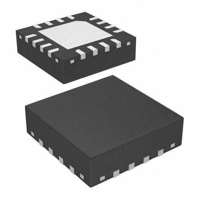
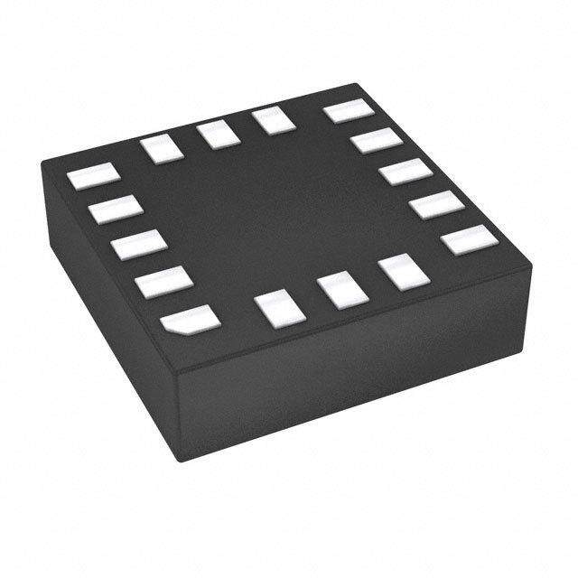
ICGOO电子元器件商城为您提供BMG160由BOSCH设计生产,在icgoo商城现货销售,并且可以通过原厂、代理商等渠道进行代购。 BMG160价格参考。BOSCHBMG160封装/规格:运动传感器 - 陀螺仪, Gyroscope X (Pitch), Y (Roll), Z (Yaw) ±125, 250, 500, 1000, 2000 12Hz ~ 230Hz I²C, SPI 12-LGA (3x3)。您可以下载BMG160参考资料、Datasheet数据手册功能说明书,资料中有BMG160 详细功能的应用电路图电压和使用方法及教程。
Bosch Sensortec的BMG160是一款高性能、低功耗的三轴陀螺仪,广泛应用于消费电子和工业领域。以下是其主要应用场景:

 1. 智能手机和平板电脑
   - BMG160可用于智能手机和平板电脑中的运动检测,支持屏幕旋转、游戏控制、增强现实(AR)以及手势识别等功能。
   - 在拍照和视频录制时,结合加速度计实现图像稳定功能(EIS,电子图像稳定)。

 2. 可穿戴设备
   - 在智能手表、健身追踪器等可穿戴设备中,BMG160用于步数计算、姿态监测、跌倒检测和活动跟踪。
   - 支持手势交互,例如通过手腕动作触发特定功能。

 3. 无人机与机器人
   - BMG160为无人机提供姿态信息,帮助其实现稳定飞行和航向控制。
   - 在机器人应用中,用于姿态估计、导航和运动控制。

 4. 虚拟现实(VR)和增强现实(AR)
   - 提供精确的头部或手部运动追踪数据,增强沉浸式体验。
   - 结合加速度计实现六自由度(6DoF)运动追踪。

 5. 室内导航与定位
   - 在GPS信号弱的环境中(如室内或地下),BMG160可通过惯性导航技术提供方向和位移信息。
   - 适用于商场导航、仓库管理和资产追踪。

 6. 智能家居与安防
   - 在智能家居设备中,用于检测门窗开合角度或家具移动。
   - 在安防系统中,监测异常振动或倾斜事件。

 7. 运动与健康监测
   - 用于跑步、游泳、骑行等运动分析,提供精确的姿态和旋转数据。
   - 在康复设备中,辅助医生评估患者的运动能力。

 8. 玩具与遥控设备
   - 在遥控车、飞机或船中,BMG160用于稳定控制和方向调整。
   - 在互动玩具中,实现基于运动的交互功能。

BMG160凭借其高精度、低噪声和低功耗特性,在上述场景中表现出色,能够满足多种应用需求。
| 参数 | 数值 |
| 产品目录 | |
| 描述 | GYROSCOPE 3-AXIS SPI/I2C SMD螺旋仪 3-Axis 3x3mm LGA-12 to 2000 deg/s 16-bit |
| 产品分类 | 陀螺仪运动与定位传感器 |
| 品牌 | Bosch Sensortec |
| 产品手册 | |
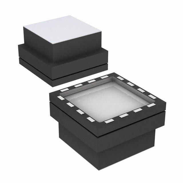
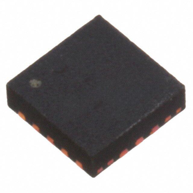
| 产品图片 |
|
| rohs | 符合RoHS无铅 / 符合限制有害物质指令(RoHS)规范要求 |
| 产品系列 | 螺旋仪,Bosch Sensortec BMG160- |
| 数据手册 | |
| 产品型号 | BMG160 |
| 产品种类 | 螺旋仪 |
| 传感轴 | X, Y, Z |
| 供应商器件封装 | 12-LGA(3x3) |
| 其它名称 | 828-1042-1 |
| 典型带宽 | 2kHz |
| 商标 | Bosch Sensortec |
| 封装 | Reel |
| 封装/外壳 | 12-VFLGA |
| 封装/箱体 | LGA-12 |
| 工作温度 | -40°C ~ 85°C |
| 工厂包装数量 | 5000 |
| 带宽 | 230 Hz |
| 数字输出-位数 | 16 bit |
| 数字输出-总线接口 | I2C, SPI |
| 最大工作温度 | + 85 C |
| 最小工作温度 | - 40 C |
| 标准包装 | 1 |
| 灵敏度 | 262.4LSB/(°/s), 131.2LSB/(°/s), 65.6LSB/(°/s), 32.8LSB/(°/s), 16.4LSB/(°/s) |
| 电压-电源 | 2.4 V ~ 3.6 V |
| 电流-电源 | 5mA |
| 电源电压-最大 | 3.6 V |
| 电源电压-最小 | 1.2 V |
| 电源电流 | 5 mA |
| 范围°/s | ±125°/s ~ ±2000°/s |
| 输出类型 | I²C, SPI |
| 零件号别名 | 0273.142.007-1NV 828-1042-1-ND 828-1042-2-ND 828-1042-6-ND |


- 商务部:美国ITC正式对集成电路等产品启动337调查
- 曝三星4nm工艺存在良率问题 高通将骁龙8 Gen1或转产台积电
- 太阳诱电将投资9.5亿元在常州建新厂生产MLCC 预计2023年完工
- 英特尔发布欧洲新工厂建设计划 深化IDM 2.0 战略
- 台积电先进制程称霸业界 有大客户加持明年业绩稳了
- 达到5530亿美元!SIA预计今年全球半导体销售额将创下新高
- 英特尔拟将自动驾驶子公司Mobileye上市 估值或超500亿美元
- 三星加码芯片和SET,合并消费电子和移动部门,撤换高东真等 CEO
- 三星电子宣布重大人事变动 还合并消费电子和移动部门
- 海关总署:前11个月进口集成电路产品价值2.52万亿元 增长14.8%
PDF Datasheet 数据手册内容提取
Data sheet BMG160 Page 1 Data sheet BMG160 Digital, triaxial gyroscope sensor Bosch Sensortec BMG160: Data sheet Document revision 1.2 Document release date 06 May 2014 Document number BST-BMG160-DS000-09 Technical reference code(s) 0 273 142 007 Notes Data in this document are subject to change without notice. Product photos and pictures are for illustration purposes only and may differ from the real product’s appearance. BST-BMG160-DS000-09 | Revision 1.2 | May 2014 Bosch Sensortec Not intended for publishing © Bosch Sensortec GmbH reserves all rights even in the event of industrial property rights. We reserve all rights of disposal such as copying and passing on to third parties. BOSCH and the symbol are regis tered trademarks of Robert Bosch GmbH, Germany. Note: Specifications within this document are subject to change without notice.
BMG160 Page 2 Data sheet BMG160 16BIT, DIGITAL, TRIAXIAL ±125°/S TO ±2000°/S GYROSCOPE SENSOR 3MM X 3MM X 0.95MM LGA PACKAGE Key features 3-axis integrated gyroscope 16 bit digital resolution Switchable full-scale ranges: in total 5 ranges V : 2.4 ... 3.6V / V : 1.2 ... 3.6V DD DDIO Interrupt engine Low power consumption <5mA Short start-up time of 30ms Wake-up time in fast power-up mode only 10ms Operating temperature: -40°C ... +85°C I2C and SPI interface (4-wire and 3-wire, SPI mode 0 and mode 3) Low-pass filters Fast and slow offset controller (FOC and SOC) Small footprint 12 pin LGA package, 3mm x 3mm x 0.95mm MSL level 1 RoHS compliant, halogen-free, Pb-free Temperture Sensor Typical applications Cell-phones Human machine interface devices Gaming Image stabilization Gesture recognition Indoor navigation General Description The BMG160 is a 3-axis angular rate sensor that is made of a surface micro machined sensing element and an evaluation ASIC. Both parts are packed into one single LGA 3.0mm x 3.0mm x 0.95mm housing. The BMG160 is designed to meet requirements for consumer applications such as image stabilization (DSC and camera-phone), gaming and pointing devices. It is capable to measure angular rates in three perpendicular room dimensions, the x-, y- and z-axis, and to provide the corresponding output signals. The BMG160 is fitted with digital bi-directional SPI and I2C interfaces for optimum system integration. The BMG160 offers a variable V voltage range from 1.2V to 3.6V and can be programmed DDIO to optimize functionality, performance and power consumption in customer specific applications. In addition it features an on-chip interrupt controller enabling motion-based applications without use of a microcontroller. BST-BMG160-DS000-09 | Revision 1.2 | May 2014 Bosch Sensortec © Bosch Sensortec GmbH reserves all rights even in the event of industrial property rights. We reserve all rights of disposal such as copying and passing on to third parties. BOSCH and the symbol are registered trademarks of Robert Bosch GmbH, Germany. Note: Specifications within this document are subject to change without notice.
BMG160 Page 3 Data sheet Index of Contents 1. SPECIFICATION ........................................................................................................................ 7 1.1 ELECTRICAL SPECIFICATION ................................................................................................. 7 1.2 ELECTRICAL AND PHYSICAL CHARACTERISTICS, MEASUREMENT PERFORMANCE ...................... 7 2. ABSOLUTE MAXIMUM RATINGS .......................................................................................... 11 2. ABSOLUTE MAXIMUM RATINGS .......................................................................................... 11 3. BLOCK DIAGRAM ................................................................................................................... 12 4. FUNCTIONAL DESCRIPTION ................................................................................................. 13 4.1 SUPPLY VOLTAGE AND POWER MANAGEMENT ..................................................................... 13 4.2 POWER MODES ................................................................................................................. 14 4.2.1 ADVANCED POWER-SAVING MODES ................................................................................................15 4.3 SENSOR DATA .................................................................................................................. 17 4.3.1 RATE DATA ...................................................................................................................................17 4.3.2 TEMPERATURE SENSOR ................................................................................................................18 4.4 ANGULAR RATE READ-OUT ................................................................................................ 18 4.5 SELF-TEST ....................................................................................................................... 18 4.6 OFFSET COMPENSATION ................................................................................................... 19 4.6.1 SLOW COMPENSATION ................................................................................................................. 19 4.6.2 FAST COMPENSATION................................................................................................................... 19 4.6.3 MANUAL COMPENSATION .............................................................................................................. 20 4.6.4 INLINE CALIBRATION ..................................................................................................................... 20 4.7 NON-VOLATILE MEMORY .................................................................................................... 21 4.8 INTERRUPT CONTROLLER .................................................................................................. 22 4.8.1 GENERAL FEATURES .....................................................................................................................22 4.8.2 MAPPING TO PHYSICAL INTERRUPT PINS (INTTYPE TO INT PIN#)......................................................23 4.8.3 ELECTRICAL BEHAVIOUR (INT PIN# TO OPEN-DRIVE OR PUSH-PULL) ................................................24 4.8.4 NEW DATA INTERRUPT ...................................................................................................................24 4.8.5 ANY-MOTION DETECTION / INTERRUPT ...........................................................................................25 4.8.6 HIGH-RATE INTERRUPT ................................................................................................................ 26 5. FIFO OPERATION ................................................................................................................... 28 5.1 FIFO OPERATING MODES ................................................................................................. 28 5.2 FIFO DATA READOUT ....................................................................................................... 29 5.2.1 EXTERNAL FIFO SYNCHRONIZATION (EFS) FOR THE GYROSCOPE ................................................. 30 5.2.2 INTERFACE SPEED REQUIREMENTS FOR FIFO USE .........................................................................31 5.2.3 FIFO FRAME COUNTER AND OVERRUN FLAG .................................................................................31 5.2.4 FIFO INTERRUPTS ........................................................................................................................32 BST-BMG160-DS000-09 | Revision 1.2 | May 2014 Bosch Sensortec © Bosch Sensortec GmbH reserves all rights even in the event of industrial property rights. We reserve all rights of disposal such as copying and passing on to third parties. BOSCH and the symbol are registered trademarks of Robert Bosch GmbH, Germany. Note: Specifications within this document are subject to change without notice.
BMG160 Page 4 Data sheet 6. REGISTER DESCRIPTION ...................................................................................................... 33 6.1 GENERAL REMARKS .......................................................................................................... 33 6.2 REGISTER MAP ................................................................................................................. 34 REGISTER 0X00 (CHIP_ID) .................................................................................................... 35 REGISTER 0X01 IS RESERVED ................................................................................................. 35 REGISTER 0X02 (RATE_X_LSB) ............................................................................................ 35 REGISTER 0X03 (RATE_X_MSB) ........................................................................................... 36 REGISTER 0X04 (RATE_Y_LSB) ............................................................................................ 36 REGISTER 0X05 (RATE_Y_MSB) ........................................................................................... 37 REGISTER 0X06 (RATE_Z_LSB) ............................................................................................ 37 REGISTER 0X07 (RATE_Z_MSB) ........................................................................................... 38 REGISTER 0X08 (TEMP) ........................................................................................................ 39 REGISTER 0X09 (INT_STATUS_0) ......................................................................................... 40 REGISTER 0X0A (INT_STATUS_1) ........................................................................................ 40 REGISTER 0X0B (INT_STATUS_2) ........................................................................................ 41 REGISTER 0X0C (INT_STATUS_3) ........................................................................................ 41 REGISTER 0X0D IS RESERVED ................................................................................................. 42 REGISTER 0X0E (FIFO_STATUS) .......................................................................................... 42 REGISTER 0X0F (RANGE) ..................................................................................................... 43 REGISTER 0X10 (BW) ............................................................................................................. 44 REGISTER 0X11 (LPM1) ......................................................................................................... 45 REGISTER 0X12 (LPM2) ......................................................................................................... 46 REGISTER 0X13 (RATE_HBW) ............................................................................................... 47 REGISTER 0X14 (BGW_SOFTRESET) ................................................................................... 47 REGISTER 0X15 (INT_EN_0) .................................................................................................. 48 REGISTER 0X16 (INT_EN_1) .................................................................................................. 48 REGISTER 0X17 (INT_MAP_0) ............................................................................................... 49 REGISTER 0X18 (INT_MAP_1) ............................................................................................... 49 REGISTER 0X19 (INT_MAP_2) ............................................................................................... 50 REGISTER 0X1A ..................................................................................................................... 50 REGISTER 0X1B ..................................................................................................................... 51 REGISTER 0X1C ..................................................................................................................... 51 REGISTER 0X1D IS RESERVED. ................................................................................................ 52 REGISTER 0X1E ..................................................................................................................... 52 REGISTERS 0X1F TO 0X20 ARE RESERVED .............................................................................. 52 BST-BMG160-DS000-09 | Revision 1.2 | May 2014 Bosch Sensortec © Bosch Sensortec GmbH reserves all rights even in the event of industrial property rights. We reserve all rights of disposal such as copying and passing on to third parties. BOSCH and the symbol are registered trademarks of Robert Bosch GmbH, Germany. Note: Specifications within this document are subject to change without notice.
BMG160 Page 5 Data sheet REGISTER 0X21 (INT_RST_LATCH) ...................................................................................... 53 REGISTER 0X22 (HIGH_TH_X) ................................................................................................ 54 REGISTER 0X23 (HIGH_DUR_X) ............................................................................................. 55 REGISTER 0X24 (HIGH_TH_Y) ................................................................................................ 55 REGISTER 0X25 (HIGH_DUR_Y) ............................................................................................. 56 REGISTER 0X26 (HIGH_TH_Z) ................................................................................................ 56 REGISTER 0X27 (HIGH_DUR_Z) ............................................................................................. 57 REGISTERS 0X28 TO 0X30 ARE RESERVED............................................................................... 57 REGISTER 0X31 (SOC) ........................................................................................................... 57 REGISTER 0X32 (A_FOC) ...................................................................................................... 58 REGISTER 0X33 (TRIM_NVM_CTRL) ..................................................................................... 59 REGISTER 0X34 (BGW_SPI3_WDT) ...................................................................................... 60 REGISTER 0X35 IS RESERVED ................................................................................................. 60 REGISTER 0X36 (OFC1) ......................................................................................................... 61 REGISTER 0X37 (OFC2) ......................................................................................................... 62 REGISTER 0X38 (OFC3) ......................................................................................................... 63 REGISTER 0X39 (OFC4) ......................................................................................................... 64 REGISTER 0X3A (TRIM_GP0) ................................................................................................ 64 REGISTER 0X3B (TRIM_GP1) ................................................................................................ 65 REGISTER 0X3C (BIST) .......................................................................................................... 65 REGISTER 0X3D (FIFO_CONFIG_0) ...................................................................................... 66 REGISTER 0X3E (FIFO_CONFIG_1) ...................................................................................... 67 REGISTER 0X3F (FIFO_DATA) ............................................................................................... 68 7. DIGITAL INTERFACES ............................................................................................................ 69 7.1 SERIAL PERIPHERAL INTERFACE (SPI) ................................................................................ 70 7.2 INTER-INTEGRATED CIRCUIT (I²C) ...................................................................................... 74 7.2.1 SPI AND I²C ACCESS RESTRICTIONS .............................................................................................77 8. PIN-OUT AND CONNECTION DIAGRAM .............................................................................. 78 8.1 PIN-OUT ........................................................................................................................... 78 8.2 CONNECTION DIAGRAM 4-WIRE SPI ................................................................................... 79 8.3 CONNECTION DIAGRAM 3-WIRE SPI ................................................................................... 80 8.4 CONNECTION DIAGRAM I2C ................................................................................................ 80 BST-BMG160-DS000-09 | Revision 1.2 | May 2014 Bosch Sensortec © Bosch Sensortec GmbH reserves all rights even in the event of industrial property rights. We reserve all rights of disposal such as copying and passing on to third parties. BOSCH and the symbol are registered trademarks of Robert Bosch GmbH, Germany. Note: Specifications within this document are subject to change without notice.
BMG160 Page 6 Data sheet 9. PACKAGE ................................................................................................................................ 81 9.1 OUTLINE DIMENSIONS ....................................................................................................... 81 9.2 SENSING AXES ORIENTATION ............................................................................................. 82 9.3 LANDING PATTERN RECOMMENDATION ............................................................................... 83 9.4 MARKING ......................................................................................................................... 84 9.4.1 MASS PRODUCTION SAMPLES ........................................................................................................84 9.4.2 ENGINEERING SAMPLES ................................................................................................................84 9.5 SOLDERING GUIDELINES .................................................................................................... 85 9.6 HANDLING INSTRUCTIONS .................................................................................................. 86 9.7 TAPE AND REEL SPECIFICATION ......................................................................................... 87 9.7.1 ORIENTATION WITHIN THE REEL .....................................................................................................88 9.7.2 ENVIRONMENTAL SAFETY ............................................................................................................. 89 9.7.3 HALOGEN CONTENT ..................................................................................................................... 89 9.7.4 INTERNAL PACKAGE STRUCTURE .................................................................................................. 89 10. LEGAL DISCLAIMER ............................................................................................................ 90 10.1 ENGINEERING SAMPLES .................................................................................................. 90 10.2 PRODUCT USE ................................................................................................................ 90 10.3 APPLICATION EXAMPLES AND HINTS ................................................................................. 90 11. DOCUMENT HISTORY AND MODIFICATION ..................................................................... 91 BST-BMG160-DS000-09 | Revision 1.2 | May 2014 Bosch Sensortec © Bosch Sensortec GmbH reserves all rights even in the event of industrial property rights. We reserve all rights of disposal such as copying and passing on to third parties. BOSCH and the symbol are registered trademarks of Robert Bosch GmbH, Germany. Note: Specifications within this document are subject to change without notice.
BMG160 Page 7 Data sheet 1. Specification If not stated otherwise, the given values are over lifetime and full performance temperature and voltage ranges, minimum/maximum values are ±3. 1.1 Electrical specification Table 1: Electrical parameter specification GYROSCOPE OPERATING CONDITIONS Parameter Symbol Condition Min Typ Max Unit Supply Voltage V 2.4 3.0 3.6 V Internal Domains DD Supply Voltage V 1.2 2.4 3.6 V I/O Domain DDIO Voltage Input V SPI & I²C 0.3V - Low Level IL DDIO Voltage Input V SPI & I²C 0.7V - High Level IH DDIO Voltage Output V = 1.2V V DDIO 0.23V - Low Level OL I = 3mA, SPI & I²C DDIO OL Voltage Output V = 1.2V V DDIO 0.8V - High Level OH I = 3mA, SPI DDIO OH 1.2 Electrical and physical characteristics, measurement performance Table 2: Electrical characteristics GYROSCOPE OPERATING CONDITIONS Parameter Symbol Condition Min Typ Max Unit 125 R °/s FS125 250 R °/s FS250 Selectable 500 Range R via serial digital °/s FS500 interface 1,000 R °/s FS1000 2,000 R °/s FS2000 BST-BMG160-DS000-09 | Revision 1.2 | May 2014 Bosch Sensortec © Bosch Sensortec GmbH reserves all rights even in the event of industrial property rights. We reserve all rights of disposal such as copying and passing on to third parties. BOSCH and the symbol are registered trademarks of Robert Bosch GmbH, Germany. Note: Specifications within this document are subject to change without notice.
BMG160 Page 8 Data sheet Supply Current in I see1 5 mA Normal Mode DD Supply Current in Fast Power- I see1 2.5 mA DDfpm up Mode Supply Current see1, digital and in Suspend - I analog 25 µA DDsum Mode (only IF active) Supply Current in Deep I see1 <5 µA Suspend - DDdsum Mode to ±1º/s of final Start-up time t value; 30 ms su from power-off From suspend- and Wake-up time t deep suspend- 30 ms wusm modes From fast power-up Wake-up time t 10 ms wufpm mode Non-volatile memory (NVM) n 15 cycles NVM write-cycles Operating T full performance -40 +85 °C Temperature A Ta=25°C, R 16.4 LSB/°/s FS2000 Ta=25°C, R 32.8 LSB/°/s FS1000 Sensitivity Ta=25°C, R 65.6 LSB/°/s FS500 Ta=25°C, R 131.2 LSB/°/s FS250 Ta=25°C, R 262.4 LSB/°/s FS125 Sensitivity Ta=25°C, R ±1 % tolerance FS2000 Sensitivity Nominal V supplies DD Change over TCS -40°C ≤ T ≤ +85°C ±0.03 %/K A Temperature R FS2000 1 Conditions of current consumption if not specified otherwise: TA=25°C, BW_Gyro=1kHz, VDD=2.4V, VDDIO=1.8V, digital protocol on, no streaming data BST-BMG160-DS000-09 | Revision 1.2 | May 2014 Bosch Sensortec © Bosch Sensortec GmbH reserves all rights even in the event of industrial property rights. We reserve all rights of disposal such as copying and passing on to third parties. BOSCH and the symbol are registered trademarks of Robert Bosch GmbH, Germany. Note: Specifications within this document are subject to change without notice.
BMG160 Page 9 Data sheet best fit straight line Nonlinearity NL ±0.05 %FS R R FS1000, FS2000 Sensitivity to acceleration stimuli g- Sensitivity 0.1 °/s/g in all three axis (frequency <20kHz) Nominal V supplies DD Zero-rate Off T =25°C, x A ±1 °/s Offset y and z Slow and fast offset cancellation off Zero- Offset Nominal V supplies DD Change over TCO -40°C ≤ T ≤ +85°C ±0.015 °/s per K A Temperature R FS2000 rms, BW=47Hz Output Noise n 0.1 °/s rms (@ 0.014°/s/√Hz) unfiltered 230 116 64 Bandwidth BW f Hz -3dB 47 32 23 12 2000 Data rate 1000 (set of x,y,z 400 Hz rate) 200 100 Data rate tolerance(set of ±0.3 % x,y,z rate) Sensitivity to stimuli Cross Axis in non-sense- ±1 % Sensitivity direction Temperature Sensor T -40 85 °C Measurement S Range BST-BMG160-DS000-09 | Revision 1.2 | May 2014 Bosch Sensortec © Bosch Sensortec GmbH reserves all rights even in the event of industrial property rights. We reserve all rights of disposal such as copying and passing on to third parties. BOSCH and the symbol are registered trademarks of Robert Bosch GmbH, Germany. Note: Specifications within this document are subject to change without notice.
BMG160 Page 10 Data sheet Temperature dT 0.5 K/LSB Sensor Slope S Temperature OT 5 ±3 K Sensor Offset S BST-BMG160-DS000-09 | Revision 1.2 | May 2014 Bosch Sensortec © Bosch Sensortec GmbH reserves all rights even in the event of industrial property rights. We reserve all rights of disposal such as copying and passing on to third parties. BOSCH and the symbol are registered trademarks of Robert Bosch GmbH, Germany. Note: Specifications within this document are subject to change without notice.
BMG160 Page 11 Data sheet 2. Absolute maximum ratings Table 3: Absolute maximum ratings Parameter Condition Min Max Units Voltage at Supply Pin V Pin -0.3 4.25 V DD (<1s) V Pin -0.3 4.25 V DDIO Voltage at any Logic Pin Non-Supply Pin -0.3 V +0.3 V DDIO Passive Storage Temp. Range ≤ 65% rel. H. -50 +150 °C None-volatile memory (NVM) T = 85°C, 10 y Data Retention after 15 cycles Duration ≤ 200µs 10,000 g Duration ≤ 1.0ms 2,000 g Mechanical Shock Free fall 1.8 m onto hard surfaces HBM, at any Pin 2 kV ESD CDM 500 V MM 200 V Note: Stress above these limits may cause damage to the device. Exceeding the specified electrical limits may affect the device reliability or cause malfunction. BST-BMG160-DS000-09 | Revision 1.2 | May 2014 Bosch Sensortec © Bosch Sensortec GmbH reserves all rights even in the event of industrial property rights. We reserve all rights of disposal such as copying and passing on to third parties. BOSCH and the symbol are registered trademarks of Robert Bosch GmbH, Germany. Note: Specifications within this document are subject to change without notice.
BMG160 Page 12 Data sheet 3. Block diagram Figure 1 shows the basic building blocks of the BMG160: Figure 1: Block diagram of BMG160 BST-BMG160-DS000-09 | Revision 1.2 | May 2014 Bosch Sensortec © Bosch Sensortec GmbH reserves all rights even in the event of industrial property rights. We reserve all rights of disposal such as copying and passing on to third parties. BOSCH and the symbol are registered trademarks of Robert Bosch GmbH, Germany. Note: Specifications within this document are subject to change without notice.
BMG160 Page 13 Data sheet 4. Functional description Note: Default values for registers can be found in chapter 6. 4.1 Supply voltage and power management The BMG160 has two distinct power supply pins: • V is the main power supply for the internal blocks; DD • V is a separate power supply pin mainly used for the supply of the interface DDIO There are no limitations on the voltage levels of both pins relative to each other, as long as each of them lies within its operating range. Furthermore, the device can be completely switched off (V = 0V) while keeping the V supply on (V > 0V) or vice versa. DD DDIO DDIO When the V supply is switched off, all interface pins (CSB, SDI, SCK, PS) must be kept DDIO close to GND potential. IO The device contains a power-on reset (POR) generator. It resets the logic part and the register values after powering-on V and V . Please note, that all application specific settings which DD DDIO are not equal to the default settings (refer to 6.2 register map), must be re-set to their designated values after POR. In case the I²C interface shall be used, a direct electrical connection between V supply and DDIO the PS pin is needed in order to ensure reliable protocol selection. For SPI interface mode the PS pin must be directly connected to GND . IO BST-BMG160-DS000-09 | Revision 1.2 | May 2014 Bosch Sensortec © Bosch Sensortec GmbH reserves all rights even in the event of industrial property rights. We reserve all rights of disposal such as copying and passing on to third parties. BOSCH and the symbol are registered trademarks of Robert Bosch GmbH, Germany. Note: Specifications within this document are subject to change without notice.
BMG160 Page 14 Data sheet 4.2 Power modes The BMG160 has 4 different power modes. Besides normal mode, which represents the fully operational state of the device, there are 3 energy saving modes: deep-suspend mode, suspend mode, and fast power up Figure 2: Block diagram of the power modes of BMG160 After power-up BMG160 is in normal mode so that all parts of the device are held powered-up and data acquisition is performed continuously. BST-BMG160-DS000-09 | Revision 1.2 | May 2014 Bosch Sensortec © Bosch Sensortec GmbH reserves all rights even in the event of industrial property rights. We reserve all rights of disposal such as copying and passing on to third parties. BOSCH and the symbol are registered trademarks of Robert Bosch GmbH, Germany. Note: Specifications within this document are subject to change without notice.
BMG160 Page 15 Data sheet In deep-suspend mode the device reaches the lowest possible power consumption. Only the interface section is kept alive. No data acquisition is performed and the content of the configuration registers is lost. Deep suspend mode is entered (left) by writing ‘1’ (‘0’) to the (0x11) deep_suspend bit. The I2C watchdog timer remains functional. The (0x11) deep_ suspend bit, the (0x34) spi3 bit, (0x34) i2c_wdt_en bit and the (0x34) i2c_wdt_sel bit are functional in deep-suspend mode. Equally the interrupt level and driver configuration registers (0x20) int1_lvl, (0x20) int1_od, (0x20) int2_lvl, and (0x20) int2_od are accessible. Still it is possible to enter normal mode by writing to the (0x14) softreset register. Please note, that all application specific settings which are not equal to the default settings (refer to 6.2 register map), must be re-set to its designated values after leaving deep-suspend mode. In suspend mode the whole analog part is powered down. No data acquisition is performed. While in suspend mode the latest rate data and the content of all configuration registers are kept. The only supported operations are reading registers as well as writing to the (0x14) softreset register. Suspend mode is entered (left) by writing ´1´ (´0´) to the (0x11) suspend bit. Bit (0x12) fast_power_up must be set to ‘0’. Although write access to registers is supported at the full interface clock speed (SCL or SCK), a waiting period must be inserted between two consecutive write cycles (please refer also to section 7.2.1). In external wake-up mode, when the device is in deep suspend mode or suspend mode, it can be woken-up by external trigger to Pin INT1/2. Register settings: Table 4 ext_trig_sel<1:0> Trigger source ‘00’ No ‘01’ INT1 pin ‘10’ INT2 pin ‘11’ SDO pin (SPI3 mode) In fast power-up mode the sensing analog part is powered down, while the drive and the digital part remains operational. No data acquisition is performed. Reading and writing registers as well as writing to the (0x14) softreset register are supported without any restrictions. The latest rate data and the content of all configuration registers are kept. Fast power-up mode is entered (left) by writing ´1´ (´0´) to the (0x11) suspend bit with bit (0x12) fast_power_up set to ‘1’. 4.2.1 Advanced power-saving modes In addition to the power modes described in Figure 2, there are other advanced power modes that can be used to optimize the power consumption of the BMG160. The power_save_mode is set by setting power_save_mode=´1´ (reg 0x12). This power mode implements a duty cycle and change between normal mode and fast-power-up mode. By setting the sleep_dur (time in ms in fast-power-up mode) (0x11 bits <1:3>) and auto_sleep_dur BST-BMG160-DS000-09 | Revision 1.2 | May 2014 Bosch Sensortec © Bosch Sensortec GmbH reserves all rights even in the event of industrial property rights. We reserve all rights of disposal such as copying and passing on to third parties. BOSCH and the symbol are registered trademarks of Robert Bosch GmbH, Germany. Note: Specifications within this document are subject to change without notice.
BMG160 Page 16 Data sheet (time in ms in normal mode) (0x12 bits <0:2>) different timings can be used. Some of these settings allow the sensor to consume less than 3mA. See also diagram below: autosleep autosleep autosleep autosleep autosleep i[mA] powerup dur dur dur dur dur NORMAL Fast Power Up sleep sleep sleep sleep sleep dur dur dur dur dur OFF t Figure 3: Duty-cycling The possible configuration for the autosleep_dur and sleep_dur are indicated in the table below: Table 5 sleep_dur<2:0> Time (ms) ‘000’ 2 ms ‘001’ 4 ms ‘010’ 5 ms ‘011’ 8 ms ‘100’ 10 ms ‘101’ 15 ms ‘110’ 18 ms ‘111’ 20 ms Table 6 autosleep_dur<2:0> Time (ms) ‘000’ Not allowed ‘001’ 4 ms ‘010’ 5 ms ‘011’ 8 ms ‘100’ 10 ms ‘101’ 15 ms ‘110’ 20 ms ‘111’ 40 ms The only restriction for the use of the power save mode comes from the configuration of the digital filter bandwidth (reg 0x10). For each Bandwidth configuration, a minimum autlosleep_dur must be ensured. For example, for Bandwidth=47Hz, the minimum autosleep_dur is 5ms. This is specified in the table below. For sleep_dur there is no restriction. BST-BMG160-DS000-09 | Revision 1.2 | May 2014 Bosch Sensortec © Bosch Sensortec GmbH reserves all rights even in the event of industrial property rights. We reserve all rights of disposal such as copying and passing on to third parties. BOSCH and the symbol are registered trademarks of Robert Bosch GmbH, Germany. Note: Specifications within this document are subject to change without notice.
BMG160 Page 17 Data sheet Table 7 bw<3:0> Bandwidth (Hz) Mini Autosleep_dur (ms) ‘0111’ 32 Hz 20 ms ‘0110’ 64 Hz 10 ms ‘0101’ 12 Hz 20 ms ‘0100’ 23 Hz 10 ms ‘0011’ 47 Hz 5 ms ‘0010’ 116 Hz 4 ms ‘0001’ 230 Hz 4 ms ‘0000’ Unfiltered (523Hz) 4 ms 4.3 Sensor data 4.3.1 Rate data The angular rate data can be read-out through addresses 0x02 through 0x07. The angular rate data is in 2’s complement form according to Table 8 below. In order to not corrupt the angular rate data, the LSB should always be read out first. Once the LSB of the x,y, or z read-out registers have been read, the MSBs are locked until the MSBs are read out. This default behavior can be switched off by setting the address 0x13 bit 6 (shadow_dis) = ‘1’. In this case there is no MSB locking, and the data is updated between each read. The burst-access mechanism provides an efficient way to read out the angular rate data in I2C or SPI mode. During a burst-access, the BMG160 automatically increments the starting read address after each byte. Any address in the user space can be used as a starting address. When the address (0x3F – fifo_data) is reached, the address counter is stopped. In the user space address range, the 0x3F – fifo_data will be continuously read out until burst read ends. It is also possible to start directly with address 0x3F. In this case, the fifo_data (0x3F) data will be read out continuously. The burst-access allows data to be transferred over the I2C bus with an up to 50% reduced data density. The angular rate data in all read-out registers is locked as long as the burst read access is active. Reading the chip angular rate registers in burst read access mode ensures that the angular rate values in all readout registers belong to the same sample. Table 8: Gyroscope Register Content for 16bit mode Decimal value Angular rate (in 2000°/s range mode) +32767 + 2000°/s … … 0 0°/s … … -32767 - 2000°/s Per default, the bandwidth of the data being read-out is limited by the internal low-pass filters according to the filter configuration. Unfiltered (high-bandwidth) data can be read out through the serial interface when the data_high_bw (0x13 bit 7) is set to ‘1’. BST-BMG160-DS000-09 | Revision 1.2 | May 2014 Bosch Sensortec © Bosch Sensortec GmbH reserves all rights even in the event of industrial property rights. We reserve all rights of disposal such as copying and passing on to third parties. BOSCH and the symbol are registered trademarks of Robert Bosch GmbH, Germany. Note: Specifications within this document are subject to change without notice.
BMG160 Page 18 Data sheet 4.3.2 Temperature sensor The width of temperature data is 8 bits given in two´s complement representation. Temperature values are available in the (0x08) temp register. The slope of the temperature sensor is 0.5K/LSB, its center temperature is 23°C [(0x08) temp = 0x00]. 4.4 Angular rate read-out Bandwidth configuration: The BMG160 processes the 2 kHz data out of the analog front end with a CIC/Decimation filter, followed by an IIR filter before sending this data to the interrupt handler. The possible decimation factors are 2, 5, 10 and 20. It is also possible to bypass these filters, and use the unfiltered 2 kHz data. The decimation factor / bandwidth of the filter can be set by setting the address space 0x10 bits<3:0> (bw<3:0>) as shown in the memory map section. 4.5 Self-test A built-in self test (BIST) facility has been implemented which provides a quick way to determine if the device is operational within the specified conditions. The BIST uses three parameters for evaluation of proper device operation: - Drive voltage regulator - Sense frontend offset regulator of x-,y- and z-channel - Quad regulator for x-,y- and z-channel If any of the three parameters is not within the limits the BIST result will be “Fail”. To trigger the BIST ´bit0´ bite_trig in address 0x3C must be set `1´. When the test is performed, bit1 bist_rdy will be ´1´. If the result is failed the bit bist_failed will be set to ´1´, otherwise stay a ´0´. bite_trig 0x3C = `1` bist_rdy = ´1´ bist_failed = ´1´ bist_failed = ´0´ à Result: Failure à Result: OK Figure 4: Flow Diagram Another possibility to get information about the sensor status is to read out rate_ok 0x3C bit4. ´1´ indicates proper sensor function, no trigger is needed for this. BST-BMG160-DS000-09 | Revision 1.2 | May 2014 Bosch Sensortec © Bosch Sensortec GmbH reserves all rights even in the event of industrial property rights. We reserve all rights of disposal such as copying and passing on to third parties. BOSCH and the symbol are registered trademarks of Robert Bosch GmbH, Germany. Note: Specifications within this document are subject to change without notice.
BMG160 Page 19 Data sheet 4.6 Offset compensation Offsets in measured signals can have several causes but they are always unwanted and disturbing in many cases. Therefore, the BMG160 offers an advanced set of four digital offset compensation methods which are closely matched to each other. These are slow, fast, and manual compensation as well as inline calibration. The compensation is performed with filtered data, and is then applied to both, unfiltered and filtered data. If necessary the result of this computation is saturated to prevent any overflow errors (the smallest or biggest possible value is set, depending on the sign). However, the registers used to read and write compensation values have a width of 8 bits. The public offset compensation registers (0x36) to (0x39) are image of the corresponding registers in the NVM. With each image update (see section 4.6 Non-volatile memory for details) the contents of the NVM registers are written to the public registers. The public register can be over-written by the user at any time. In case an internally computed compensation value is too small or too large to fit into the corresponding register, it is saturated in order to prevent an overflow error. For every axes an offset up to 125°/s with 12 bits full resolution can be calibrated (resolution 0.06°/s). The modes will be controlled using SPI/I2C commands. By writing ´1´ to the (0x21) offset_reset bit, all dynamic (fast & slow) offset compensation registers are reset to zero. 4.6.1 Slow compensation In slow regulation mode, the rate data is monitored permanently. If the rate data is above 0°/s for a certain period of time, an adjustable rate is subtracted by the offset controller. This procedure of monitoring the rate data and subtracting of the adjustable rate at a time is repeated continuously. Thus, the output of the offset converges to 0°/s. The slow regulation can be enabled through the slow_offset_en_x/y/z (0x31 <0:2>) bits for each axis. The slow offset cancellation will work for filtered and unfiltered data (slow_offset_unfilt (0x1A <5>); slow_offset_unfilt=1 à unfiltered data are selected) Slow Offset cancellation settings are the adjustable rate (slow offset_th 0x31 <7:6>) and the time period ( slow_offset_dur 0x31 <5:3>) 4.6.2 Fast compensation A fast offset cancellation controller is implemented in BMG160. The fast offset cancellation process is triggerable via SPI/I2C. The fast offset cancellation can be enabled through the fast_offset_en_x/y/z (0x32 <0:2>) bits for each axis. The enable bits will not start the fast offset cancellation! The fast offset cancellation has to be started by setting the fast_offset_en (0x32 <3>) bit. Afterwards the algorithm will start and if the algorithm is finished the fast_offset_en (0x32 <3>) will be reset to 0. BST-BMG160-DS000-09 | Revision 1.2 | May 2014 Bosch Sensortec © Bosch Sensortec GmbH reserves all rights even in the event of industrial property rights. We reserve all rights of disposal such as copying and passing on to third parties. BOSCH and the symbol are registered trademarks of Robert Bosch GmbH, Germany. Note: Specifications within this document are subject to change without notice.
BMG160 Page 20 Data sheet The fast offset cancellation will work for filtered and unfiltered data (fast_offset_unfilt (0x1B <7>); fast_offset_unfilt=1 à unfiltered data are selected) The fast offset cancellation parameters are fast_offset_wordlength (0x32 <5:4>) The sample rate for the fast offset cancellation corresponds to the sample rate of the selected bandwidth. For unfiltered data and bandwidth settings 0-2 the sample rate for the fast offset cancellation will be 400Hz. The resolution of the calculated offset values for the fast offset compensation depends on the, range setting being less accurate for higher range (e.g. range=2000°/s).Therefore we recommend a range setting of range=125°/s for fast offset compensation. 4.6.3 Manual compensation The contents of the public compensation registers (0x36 … 0x39) offset_x/y/z can be set manually via the digital interface. It is recommended to write into these registers directly after a new data interrupt has occurred in order not to disturb running offset computations. Writing to the offset compensation registers is not allowed while the fast compensation procedure is running. 4.6.4 Inline calibration For certain applications, it is often desirable to calibrate the offset once and to store the compensation values permanently. This can be achieved by using one of the aforementioned offset compensation methods to determine the proper compensation values and then storing these values permanently in the NVM. See section 4.7 Non-volatile memory for details of the storing procedure. Each time the device is reset, the compensation values are loaded from the non-volatile memory into the image registers and used for offset compensation until they are possibly overwritten using one of the other compensation methods. BST-BMG160-DS000-09 | Revision 1.2 | May 2014 Bosch Sensortec © Bosch Sensortec GmbH reserves all rights even in the event of industrial property rights. We reserve all rights of disposal such as copying and passing on to third parties. BOSCH and the symbol are registered trademarks of Robert Bosch GmbH, Germany. Note: Specifications within this document are subject to change without notice.
BMG160 Page 21 Data sheet 4.7 Non-volatile memory The entire memory of the BMG160 consists of three different kinds of registers: hard-wired, volatile, and non-volatile. Part of it can be both read and written by the user. Access to non- volatile memory is only possible through (volatile) image registers. Altogether, there are eight registers (octets) with NVM backup which are accessible by the user. The addresses of the image registers range from 0x36 to 0x3B. While the addresses up to 0x39 are used for offset compensation (see 4.4 Offset Compensation), addresses 0x3A and 0x3B are general purpose registers not linked to any sensor-specific functionality. The content of the NVM is loaded to the image registers after a reset (either POR or softreset) or after a user request which is performed by writing ´1´ to the write-only bit (0x33) nvm_load. As long as the image update is in progress, bit (0x33) nvm_rdy is ´0´, otherwise it is ´1´. In order to read out the correct values (after NVM loading) waiting time is min. 1ms. The image registers can be read and written like any other register. Writing to the NVM is a three-step procedure: 1. Write the new contents to the image registers. 2. Write ´1´ to bit (0x33) nvm_prog_mode in order to unlock the NVM. 3. Write ´1´ to bit (0x33) nvm_prog_trig and keep ´1´ in bit (0x33) nvm_prog_mode in order to trigger the write process. Writing to the NVM always renews the entire NVM contents. It is possible to check the write status by reading bit (0x33) nvm_rdy. While (0x33) nvm_rdy = ´0´, the write process is still in progress; if (0x33) nvm_rdy = ´1´, then writing is completed. As long as the write process is ongoing, no change of power mode and image registers is allowed. Also, the NVM write cycle must not be initiated while image registers are updated, in suspend mode. Please note that the number of permitted NVM write-cycles is limited as specified in Table 2. The number of remaining write-cycles can be obtained by reading bits (0x33) nvm_remain. BST-BMG160-DS000-09 | Revision 1.2 | May 2014 Bosch Sensortec © Bosch Sensortec GmbH reserves all rights even in the event of industrial property rights. We reserve all rights of disposal such as copying and passing on to third parties. BOSCH and the symbol are registered trademarks of Robert Bosch GmbH, Germany. Note: Specifications within this document are subject to change without notice.
BMG160 Page 22 Data sheet 4.8 Interrupt controller The BMG160 is equipped with 3 programmable interrupt engines. Each interrupt can be independently enabled and configured. If the trigger condition of an enabled interrupt is fulfilled, the corresponding status bit is set to ´1´ and the selected interrupt pin is activated. The BMG160 provides two interrupt pins, INT1 and INT2; interrupts can be freely mapped to any of these pins. The state of a specific interrupt pin is derived from a logic ´or´ combination of all interrupts mapped to it. The interrupt status registers are updated when a new data word is written into the rate data registers. If an interrupt is disabled, all active status bits associated with it are immediately reset. Gyro Interrupts are fully functional in normal mode, only. Interrupts are limited in their functionality in other operation modes. Please contact our technical support for further assistance. 4.8.1 General features An interrupt is cleared depending on the selected interrupt mode, which is common to all interrupts. There are three different interrupt modes: non-latched, latched, and temporary. The mode is selected by the (0x21) latch_int bits according to Table 9. Table 9: Interrupt mode selection (0x21) Interrupt mode latch_int 0000b non-latched 0001b temporary, 250ms 0010b temporary, 500ms 0011b temporary, 1s 0100b temporary, 2s 0101b temporary, 4s 0110b temporary, 8s 0111b latched 1000b non-latched 1001b temporary, 250µs 1010b temporary, 500µs 1011b temporary, 1ms 1100b temporary, 12.5ms 1101b temporary, 25ms 1110b temporary, 50ms 1111b latched An interrupt is generated if its activation condition is met. It can not be cleared as long as the activation condition is fulfilled. In the non-latched mode the interrupt status bit and the selected pin (the contribution to the ´or´ condition for INT1 and/or INT2) are cleared as soon as the BST-BMG160-DS000-09 | Revision 1.2 | May 2014 Bosch Sensortec © Bosch Sensortec GmbH reserves all rights even in the event of industrial property rights. We reserve all rights of disposal such as copying and passing on to third parties. BOSCH and the symbol are registered trademarks of Robert Bosch GmbH, Germany. Note: Specifications within this document are subject to change without notice.
BMG160 Page 23 Data sheet activation condition is no more valid. Exception to this behavior is the new data interrupt, which is automatically reset after a fixed time. In latched mode an asserted interrupt status and the selected pin are cleared by writing ´1´ to bit (0x21) reset_int. If the activation condition still holds when it is cleared, the interrupt status is asserted again with the next change of the rate registers. In the temporary mode an asserted interrupt and selected pin are cleared after a defined period of time. The behaviour of the different interrupt modes is shown graphically in Figure 5. The timings in this mode are subject to the same tolerances as the bandwidths (see Table 2). internal signal from interrupt engine interrupt output non-latched latch period temporary latched Figure 5: Interrupt modes 4.8.2 Mapping to physical interrupt pins (inttype to INT Pin#) Registers (0x17) to (0x19) are dedicated to mapping of interrupts to the interrupt pins “INT1” or “INT2”. Setting (0x17) int1_”inttype” to ´1´ (´0´) maps (unmaps) “inttype” to pin “INT1”. Correspondingly setting (0x19) int2_”inttype” to ´1´ (´0´) maps (unmaps) “inttype” to pin “INT2”. Note: “inttype” has to be replaced with the precise notation, given in the memory map in chapter 6. BST-BMG160-DS000-09 | Revision 1.2 | May 2014 Bosch Sensortec © Bosch Sensortec GmbH reserves all rights even in the event of industrial property rights. We reserve all rights of disposal such as copying and passing on to third parties. BOSCH and the symbol are registered trademarks of Robert Bosch GmbH, Germany. Note: Specifications within this document are subject to change without notice.
BMG160 Page 24 Data sheet 4.8.3 Electrical behaviour (INT pin# to open-drive or push-pull) Both interrupt pins can be configured to show the desired electrical behaviour. The ´active´ level of each interrupt pin is determined by the (0x16) int1_lvl and (0x16) int2_lvl bits. If (0x16) int1_lvl = ´1´ (´0´) / (0x16) int2_lvl = ´1´ (´0´), then pin “INT1” / pin “INT2” is active ´1´ (´0´). The characteristic of the output driver of the interrupt pins may be configured with bits (0x16) int1_od and (0x16) int2_od. By setting bits (0x16) int1_od / (0x16) int2_od to ´1´, the output driver shows open-drive characteristic, by setting the configuration bits to ´0´, the output driver shows push-pull characteristic. When open-drive characteristic is selected in the design, external pull-up or pull-down resistor should be applied according the int_lvl configuration. 4.8.4 New data interrupt This interrupt serves for synchronous reading of angular rate data. It is generated after storing a new value of z-axis angular rate data in the data register. The interrupt is cleared automatically after 280-400 µs (depending on Interrupt settings). The interrupt mode of the new data interrupt is fixed to non-latched. It is enabled (disabled) by writing ´1´ (´0´) to bit (0x15) data_en. The interrupt status is stored in bit (0x0A) data_int. BST-BMG160-DS000-09 | Revision 1.2 | May 2014 Bosch Sensortec © Bosch Sensortec GmbH reserves all rights even in the event of industrial property rights. We reserve all rights of disposal such as copying and passing on to third parties. BOSCH and the symbol are registered trademarks of Robert Bosch GmbH, Germany. Note: Specifications within this document are subject to change without notice.
BMG160 Page 25 Data sheet 4.8.5 Any-motion detection / Interrupt Any-motion (slope) detection uses the slope between successive angular rate signals to detect changes in motion. An interrupt is generated when the slope (absolute value of angular rate difference) exceeds a preset threshold. It is cleared as soon as the slope falls below the threshold. The principle is made clear in Figure 6. angular rate rate(t0) rate(t0−1/(4*fs)) time slope(t0)=gyro(t0)−gyro(t0−1/(2*bw)) slope slope_th time slope_dur slope_dur INT time Figure 6 : Principle of any-motion detection The threshold is defined through register (0x1B) any_th. In terms of scaling 1 LSB of (0x1B) any_th corresponds to 1 °/s in 2000°/s-range (0.5°/s in 1000°/s-range, 0.25°/s in 500°/s -range …). Therefore the maximum value is 125°/s in 2000°/s-range (62.5°/s 1000°/s-range, 31.25 in 500°/s -range …). The time difference between the successive angular rate signals depends on the selected update rate(fs) which is coupled to the bandwidth and equates to 1/(4*fs) (t=1/(4*fs)). For bandwidhth settings with an update rate higher than 400Hz (bandwidth =0,1,2) fs is set to 400Hz. In order to suppress false triggers, the interrupt is only generated (cleared) if a certain number N of consecutive slope data points is larger (smaller) than the slope threshold given by (0x1B) any_th. This number is set by the (0x1C) any_dursample bits. It is N = [(0x1C) any_dursample+ 1]*4 for (0x1C). N is set in samples. Thus the time is scaling with the update rate (fs). Example: (0x1C) slope_dur = 00b, …, 11b = 4 samples, …, 16 samples. BST-BMG160-DS000-09 | Revision 1.2 | May 2014 Bosch Sensortec © Bosch Sensortec GmbH reserves all rights even in the event of industrial property rights. We reserve all rights of disposal such as copying and passing on to third parties. BOSCH and the symbol are registered trademarks of Robert Bosch GmbH, Germany. Note: Specifications within this document are subject to change without notice.
BMG160 Page 26 Data sheet 4.8.5.1 Enabling (disabling) for each axis Any-motion detection can be enabled (disabled) for each axis separately by writing ´1´ (´0´) to bits (0x1C) any_en_x, (0x1C) any_en_y, (0x1C) any_en_z. The criteria for any-motion detection are fulfilled and the Any-Motion interrupt is generated if the slope of any of the enabled axes exceeds the threshold (0x1B) any_th for [(0x1C) slope_dur +1]*4 consecutive times. As soon as the slopes of all enabled axes fall or stay below this threshold for [(0x1C) slope_dur +1]*4 consecutive times the interrupt is cleared unless interrupt signal is latched. 4.8.5.2 Axis and sign information of slope / any motion interrupt The interrupt status is stored in bit (0x09) any_int. The Any-motion interrupt supplies additional information about the detected slope. The axis which triggered the interrupt is given by that one of bits (0x0B) any_first_x, (0x0B) any_first_y, (0x0B) any_first_z that contains a value of ´1´. The sign of the triggering slope is held in bit (0x0B) any_sign until the interrupt is retriggered. If (0x0B) slope_sign = ´1´ (´0´), the sign is positive (negative). 4.8.6 High-Rate interrupt This interrupt is based on the comparison of angular rate data against a high-rate threshold for the detection of shock or other high-angular rate events. The principle is made clear in Figure 7 below: Figure 7 The high-rate interrupt is enabled (disabled) per axis by writing ´1´ (´0´) to bits (0x22) high_en_x, (0x24) high_en_y, and (0x26) high_en_z, respectively. The high-rate threshold is set through the (0x22) high_th_x register, (0x24) high_th_y register and (0x26) high_th_z for the corresponding axes. The meaning of an LSB of (0x22/24/26) high_th_x/y/z depends on the selected °/s-range: it corresponds to 62.5°/s in 2000°/s-range, 31.25°/s in 1000°/s-range, 15.625°/s in 500°/s -range …). The high_th_x/y/z register setting 0 corresponds to 62.26°/s in 2000°/s-range, 31.13°/s in 1000°/s-range, 15.56°/s in 500°/s-range …. Therefore the maximum value is 1999.76°/s in 2000°/s-range (999.87°/s 1000°/s-range, 499.93°/s in 500°/s -range …). BST-BMG160-DS000-09 | Revision 1.2 | May 2014 Bosch Sensortec © Bosch Sensortec GmbH reserves all rights even in the event of industrial property rights. We reserve all rights of disposal such as copying and passing on to third parties. BOSCH and the symbol are registered trademarks of Robert Bosch GmbH, Germany. Note: Specifications within this document are subject to change without notice.
BMG160 Page 27 Data sheet A hysteresis can be selected by setting the (0x22/24/26) high_hy_x/y/z bits. Analogously to (0x22/24/26) high_th_x/y/z, the meaning of an LSB of (0x22/24/26) high_hy_x/y/z bits is °/s- range dependent: The high_hy_x/y/z register setting 0 corresponds to an angular rate difference of 62.26°/s in 2000°/s-range, 31.13°/s in 1000°/s-range, 15.56°/s in 500°/s-range …. The meaning of an LSB of (0x22/24/26) high_hy_x/y/z depends on the selected °/s-range too: it corresponds to 62.5°/s in 2000°/s-range, 31.25°/s in 1000°/s-range, 15.625°/s in 500°/s -range …). The high-rate interrupt is generated if the absolute value of the angular rate of at least one of the enabled axes (´or´ relation) is higher than the threshold for at least the time defined by the (0x23/25/27) high_dur_x/y/z register. The interrupt is reset if the absolute value of the angular rate of all enabled axes (´and´ relation) is lower than the threshold minus the hysteresis. In bit (0x09) high_int the interrupt status is stored. The relation between the content of (0x23/25/27) high_dur_x/y/z and the actual delay of the interrupt generation is delay [ms] = [(0x23/25727) high_dur_x/y/z + 1] • 2.5 ms. Therefore, possible delay times range from 2.5 ms to 640 ms. 4.8.6.1 Axis and sign information of high-rate interrupt The axis which triggered the interrupt is indicated by bits (0x0C) high_first_x, (0x0C) high_first_y, and (0x0C) high_first_z. The bit corresponding to the triggering axis contains a ´1´ while the other bits hold a ´0´. These bits are cleared together with clearing the interrupt status. The sign of the triggering angular rate is stored in bit (0x0C) high_sign. If (0x0C) high_sign = ´1´ (´0´), the sign is positive (negative). BST-BMG160-DS000-09 | Revision 1.2 | May 2014 Bosch Sensortec © Bosch Sensortec GmbH reserves all rights even in the event of industrial property rights. We reserve all rights of disposal such as copying and passing on to third parties. BOSCH and the symbol are registered trademarks of Robert Bosch GmbH, Germany. Note: Specifications within this document are subject to change without notice.
BMG160 Page 28 Data sheet 5. FIFO Operation 5.1 FIFO Operating Modes The BMG160 features an integrated FIFO memory capable of storing up to 100 frames of data in FIFO mode. Each frame consists of three 16-bit rate_x,y,z data words, and 16 bits of interrupt data sampled at the same point in time. The FIFO is a buffer memory which can be configured to operate in the following modes: FIFO Mode: In FIFO mode the X, Y, and Z rate data are stored in the buffer memory. A watermark interrupt can be enabled, which is triggered when the buffer is filled to a configurable level. The buffer will be continuously filled up until the last slot. When the buffer is full the data collection is stopped, and all additional samples are ignored. The buffer has a depth of 100 frames. STREAM Mode: Is STREAM mode the X, Y, and Z rate data is stored in the buffer until it is full. The buffer has a depth of 99 frames. When the buffer is full the data collection continues and old data are discarded in a wrap-around manner. A watermark interrupt can be enabled, which is triggered when the buffer is filled to a configurable level. BYPASS Mode: In bypass mode, only the current sensor data can be read out from the FIFO address. Essentially, the FIFO behaves like the STREAM mode with a depth of 1. The FIFO operating mode is selected with the address 0x3E bits<7:6> (mode<1:0>) according to Table 10. Register mode<1:0> will always contain the current operating mode. Writing to the mode<1:0> register clears / resets the buffer. Table 10: FIFO operating mode selection Address: 0x3E FIFO bits<7:6> Function Mode mode<1:0> ‘00’ (Default) BYPASS buffer depth of 1 frame; old data are discarded ‘01’ FIFO data collection stops when buffer is full (100 frames) when buffer full: sampling continues, old data ‘10’ STREAM discarded ‘11’ reserved BST-BMG160-DS000-09 | Revision 1.2 | May 2014 Bosch Sensortec © Bosch Sensortec GmbH reserves all rights even in the event of industrial property rights. We reserve all rights of disposal such as copying and passing on to third parties. BOSCH and the symbol are registered trademarks of Robert Bosch GmbH, Germany. Note: Specifications within this document are subject to change without notice.
BMG160 Page 29 Data sheet 5.2 FIFO Data Readout The FIFO stores the data that are also available at the addresses 0x07 – 0x02 (gyro readout registers rate_x,y,z_msb,lsb). Thus, all configuration settings apply to the FIFO data as well as to the gyro data readout registers. The FIFO can be read out from the address 0x3F bits<7:0> (fifo_data<7:0>). The readout can be performed by using burst mode. During burst mode readout from register fifo_data<7:0>, the read address counter is not incremented, effectively trapping the address counter. The trapping will also happen if burst read starts at addresses below the fifo_data<7:0> register. A single burst can read out one or more frames at a time. If a frame is not read completely due to an incomplete read operation, the remaining part of the frame is lost. In this case the FIFO aligns to the next frame during the next read operation. The address 0x3E bits<1:0> (data_select<1:0>) allows the user to select the data stored in the FIFO according to Table 11. Writing to data_select<1:0> clears the FIFO buffer. Table 11: FIFO data selection Address: 0x3E bits<1:0> data_select data of axis stored in FIFO ‘00’ (Default) X,Y,Z ‘01’ X only ‘10’ Y only ‘11’ Z only Address: 0x3D bit 7 tag Interrupt data stored in FIFO ‘0’ Default) Do not collect Interrupts ‘1’ collect Interrupts If all axes and tag are enabled, the format of the data read-out from register fifo_data<7:0> is as follows: Int. status Bits … X LSB X MSB Y LSB Y MSB Z LSB Z MSB Int_status 0 Int_status 1 Frame 1 ( 8 Bytes) If only one axis is enabled (and tag is disabled), the format of the data read-out from register fifo_data<7:0> is as follows (example shown: Y-axis only, other axis are equivalent). The buffer depth of the FIFO is independent of the fact whether all or a single axis have been selected. … Y LSB Y MSB Y LSB Y MSB Frame 1 Frame 2 BST-BMG160-DS000-09 | Revision 1.2 | May 2014 Bosch Sensortec © Bosch Sensortec GmbH reserves all rights even in the event of industrial property rights. We reserve all rights of disposal such as copying and passing on to third parties. BOSCH and the symbol are registered trademarks of Robert Bosch GmbH, Germany. Note: Specifications within this document are subject to change without notice.
BMG160 Page 30 Data sheet 5.2.1 External FIFO synchronization (EFS) for the gyroscope In addition to the explained data format for the angular rate and interrupt data, the FIFO of the gyroscope features a mode that allows the precise synchronization of external event with the gyroscope angular rate and gyroscope interrupts saved in the internal FIFO. This synchronization can be used for example for image and video stabilization applications. The EFS Mode can be used in the operating modes FIFO-Mode and STREAM-Mode but not in BYPASS-Mode. In order to use the EFS capability, any of the gyroscope interrupt pins (INT1 or INT2) can be reconfigured to act as EFS-pin, but not both. In addition, the EFS-Mode has to be enabled. The so configured interrupt pin will then behave as an input pin and not as an interrupt pin. The working principle is shown in below figure: EFS-pin FIFO Z(0) 0 0 1 1 1 0 0 Timing diagram for external FIFO synchronization. EFS-pin is the Interrupt pin configured as EFS-Mode. FIFO z(0) is the least significant bit of the z-axis gyro data stored in the FIFO. In order to enable the EFS-Mode the register (0x34) bit<5> must be set to “1”. To select the INT2 pin as EFS-pin, set the register (0x34) bit<4> to “1”. To select the INT1 pin as EFS-pin, set the register (0x34) bit<4> to “0”. In this Mode, the least significant bit of the z-axis is used as tag-bit, therefore losing its meaning as gyroscope data bit. The remaining 15 bits of the z-axis gyroscope data keep the same meaning as in standard mode. Once the EFS-pin is set to high level, the next FIFO word will be marked with an EFS-tag (z- axis LSB = 1). While the EFS-pin is kept at a High level, the corresponding FIFO words would be always marked with an EFS-tag. After the EFS-pin is reset to low level, the immediate next FIFO word could still be marked with the EFS-tag and only after this word, the next EFS-tag will be reset (z-axis LSB=0). This is shown in the above diagram. The EFS-tag synchronizes external events with the same time precision as the FIFO update rate. Therefore update rate of the EFS-tag is determined by the output data rate and can be set from 100Hz up to 2,000Hz. For more information consult the register (0x10) (BW) in the register description. BST-BMG160-DS000-09 | Revision 1.2 | May 2014 Bosch Sensortec © Bosch Sensortec GmbH reserves all rights even in the event of industrial property rights. We reserve all rights of disposal such as copying and passing on to third parties. BOSCH and the symbol are registered trademarks of Robert Bosch GmbH, Germany. Note: Specifications within this document are subject to change without notice.
BMG160 Page 31 Data sheet 5.2.2 Interface speed requirements for FIFO use In order to use the FIFO effectively, larger blocks of data need to be read out quickly. Depending on the output data rate of the sensor, this can impose requirements on the interface. The output data rate of the BMG160 is determined by the filter configuration (see chapter 6.2). What interface speed is required depends on the selected rate. For an I2C speed of 400 kHz, every filter mode can be used. For an I2C speed of 200 kHz, only modes with an output data rate of 1 KHz and below are recommended. For an I2C speed of 100 kHz, only modes with an output data rate of 400 Hz and below are recommended. 5.2.3 FIFO Frame Counter and Overrun Flag The address 0x0E bits<6:0> (frame_counter<6:0>) indicate the current fill level of the buffer. If additional frames are written to the buffer although the FIFO is full, the address 0x0E bit 7 (overrun flag) is set. If the FIFO is reset, the FIFO fill level indicated in the frame_counter<6:0> is set to ‘0’ and the overrun flag is reset each time a write operation happens to the FIFO configuration registers. The overrun bit is not reset when the FIFO fill level frame_counter<6:0> has decremented to ‘0’ due to reading from the fifo_data<7:0> register. BST-BMG160-DS000-09 | Revision 1.2 | May 2014 Bosch Sensortec © Bosch Sensortec GmbH reserves all rights even in the event of industrial property rights. We reserve all rights of disposal such as copying and passing on to third parties. BOSCH and the symbol are registered trademarks of Robert Bosch GmbH, Germany. Note: Specifications within this document are subject to change without notice.
BMG160 Page 32 Data sheet 5.2.4 FIFO Interrupts The FIFO controller has the capability to issue two different interrupt events, the FIFO-full and the watermark event. Generally the FIFO-full and watermark interrupts are functional in all non- composite modes, including BYPASS. They are not functional. The watermark interrupt is asserted when the fill level in the buffer has reached the frame number defined by the h2o_mrk_lvl_trig_ret<6:0> register. In order to enable the watermark interrupt, the fifo_en bit fifo_wm_en, as well as one or both of the int1_fifo or int2_fifo bits must be set. The status of the watermark interrupt may be read back through the address 0x0A bit 4 (fifo_int) status bit. Writing to the h2o_mrk_lvl_trig_ret<6:0> register clears the FIFO buffer. The FIFO-full interrupt is the second interrupt capability associated with the FIFO. The FIFO-full interrupt is asserted when the buffer has been fully filled with samples. In FIFO mode this occurs 100 samples, in STREAM mode 99 samples, and in BYPASS mode 1 sample after the buffer has been cleared. In order to enable the watermark interrupt, the fifo_en bit as well as one or both of the int1_full or int2_full bits must be set also. The status of the full interrupt may be read back through the fifo_int status bit. Table 12: Interrupt configuration bits relevant for the FIFO controller Register Address h2o_mrk_lvl_trig_ret<6:0> 0x3D bits<6:0> fifo_en 0x15 bit 6 fifo_wm_en 0x1E bit 7 int1_fifo 0x18 bit 2 int2_fifo 0x18 bit 5 BST-BMG160-DS000-09 | Revision 1.2 | May 2014 Bosch Sensortec © Bosch Sensortec GmbH reserves all rights even in the event of industrial property rights. We reserve all rights of disposal such as copying and passing on to third parties. BOSCH and the symbol are registered trademarks of Robert Bosch GmbH, Germany. Note: Specifications within this document are subject to change without notice.
BMG160 Page 33 Data sheet 6. Register description 6.1 General remarks The entire communication with the device is performed by reading from and writing to registers. Registers have a width of 8 bits; they are mapped to a common space of 64 addresses from (0x00) up to (0x3F). Within the used range there are several registers which are either completely or partially marked as ‘reserved’. Any reserved bit is ignored when it is written and no specific value is guaranteed when read. It is recommended not to use registers at all which are completely marked as ‘reserved’. Furthermore it is recommended to mask out (logical and with zero) reserved bits of registers which are partially marked as reserved. Registers with addresses from (0x00) up to (0x0E) are read-only. Any attempt to write to these registers is ignored. There are bits within some registers that trigger internal sequences. These bits are configured for write-only access, e. g. (0x21) reset_int or the entire (0x14) softreset register, and read as value ´0´. BST-BMG160-DS000-09 | Revision 1.2 | May 2014 Bosch Sensortec © Bosch Sensortec GmbH reserves all rights even in the event of industrial property rights. We reserve all rights of disposal such as copying and passing on to third parties. BOSCH and the symbol are registered trademarks of Robert Bosch GmbH, Germany. Note: Specifications within this document are subject to change without notice.
BMG160 Page 34 Data sheet 6.2 Register map RAdedgrisetsesr bit7 bit6 bit5 bit4 bit3 bit2 bit1 bit0 AccessReset Value 0x3F fifo_data[7] fifo_data[6] fifo_data[5] fifo_data[4] fifo_data[3] fifo_data[2] fifo_data[1] fifo_data[0] ro 0x00 0x3E mode[1] mode[0] data_select[1] data_select[0] w/r 0x00 0x3D tag h2o_mrk_lvl_trig_ret[6] h2o_mrk_lvl_trig_ret[5] h2o_mrk_lvl_trig_ret[4] h2o_mrk_lvl_trig_ret[3] h2o_mrk_lvl_trig_ret[2] h2o_mrk_lvl_trig_ret[1] h2o_mrk_lvl_trig_ret[0] w/r 0x00 0x3C rate_ok bist_fail bist_rdy trig_bist ro N/A 0x3B gp0[11] gp0[10] gp0[9] gp0[8] gp0[7] gp0[6] gp0[5] gp0[4] w/r N/A 0x3A gp0[3] gp0[2] gp0[1] gp0[0] offset_x[1] offset_x[0] offset_y[0] offset_z[0] w/r N/A 0x39 offset_z[11] offset_z[10] offset_z[9] offset_z[8] offset_z[7] offset_z[6] offset_z[5] offset_z[4] w/r N/A 0x38 offset_y[11] offset_y[10] offset_y[9] offset_y[8] offset_y[7] offset_y[6] offset_y[5] offset_y[4] w/r N/A 0x37 offset_x[11] offset_x[10] offset_x[9] offset_x[8] offset_x[7] offset_x[6] offset_x[5] offset_x[4] w/r N/A 0x36 offset_x[3] offset_x[2] offset_y[3] offset_y[2] offset_y[1] offset_z[3] offset_z[2] offset_z[1] w/r N/A 0x35 w/r 0x00 0x34 ext_fifo_s_en ext_fifo_s_sel burst_same_en i2c_wdt_en i2c_wdt_sel spi3 w/r 0x00 0x33 nvm_remain[3] nvm_remain[2] nvm_remain[1] nvm_remain[0] nvm_load nvm_rdy nvm_prog_trig nvm_prog_mode w/r 0x00 0x32 auto_offset_wordlength[1] auto_offset_wordlength[0] fast_offset_wordlength[1] fast_offset_wordlength[0] fast_offset_en fast_offset_en_z fast_offset_en_y fast_offset_en_x w/r 0xC0 0x31 slow_offset_th[1] slow_offset_th[0] slow_offset_dur[2] slow_offset_dur[1] slow_offset_dur[0] slow_offset_en_z slow_offset_en_y slow_offset_en_x w/r 0x60 0x30 w/r 0xE8 0x2F w/r 0xE0 0x2E w/r 0x81 0x2D w/r 0x40 0x2C w/r 0x42 0x2B w/r 0x22 0x2A w/r 0xE8 0x29 w/r 0x19 0x28 w/r 0x24 0x27 high_dur_z[7] high_dur_z[6] high_dur_z[5] high_dur_z[4] high_dur_z[3] high_dur_z[2] high_dur_z[1] high_dur_z[0] w/r 0x19 0x26 high_hy_z[1] high_hy_z[0] high_th_z[4] high_th_z[3] high_th_z[2] high_th_z[1] high_th_z[0] high_en_z w/r 0x02 0x25 high_dur_y[7] high_dur_y[6] high_dur_y[5] high_dur_y[4] high_dur_y[3] high_dur_y[2] high_dur_y[1] high_dur_y[0] w/r 0x19 0x24 high_hy_y[1] high_hy_y[0] high_th_y[4] high_th_y[3] high_th_y[2] high_th_y[1] high_th_y[0] high_en_y w/r 0x02 0x23 high_dur_x[7] high_dur_x[6] high_dur_x[5] high_dur_x[4] high_dur_x[3] high_dur_x[2] high_dur_x[1] high_dur_x[0] w/r 0x19 0x22 high_hy_x[1] high_hy_x[0] high_th_x[4] high_th_x[3] high_th_x[2] high_th_x[1] high_th_x[0] high_en_x w/r 0x02 0x21 reset_int offset_reset latch_status_bits latch_int[3] latch_int[2] latch_int[1] latch_int[0] w/r 0x00 0x20 w/r 0x00 0x1F w/r 0x28 0x1E fifo_wm_en w/r 0x08 0x1D w/r 0xC9 0x1C awake_dur[1] awake_dur[0] any_dursample[1] any_dursample[0] any_en_z any_en_y any_en_x w/r 0xA0 0x1B fast_offset_unfilt any_th[6] any_th[5] any_th[4] any_th[3] any_th[2] any_th[1] any_th[0] w/r 0x04 0x1A slow_offset_unfilt high_unfilt_data any_unfilt_data w/r 0x00 0x19 int2_high int2_any wo 0x00 0x18 int2_data int2_fast_offset int2_fifo int2_auto_offset int1_auto_offset int1_fifo int1_fast_offset int1_data w/r 0x00 0x17 int1_high int1_any w/r 0x00 0x16 int2_od int2_lvl int1_od int1_lvl w/r 0x0F 0x15 data_en fifo_en auto_offset_en w/r 0x00 0x14 softreset[7] softreset[6] softreset[5] softreset[4] softreset[3] softreset[2] softreset[1] softreset[0] wo 0x00 0x13 data_high_bw shadow_dis wo 0x00 0x12 fast_powerup power_save_mode ext_trig_sel[1] ext_trig_sel[0] autosleep_dur[2] autosleep_dur[1] autosleep_dur[0] w/r 0x00 0x11 suspend deep_suspend sleep_dur[2] sleep_dur[1] sleep_dur[0] w/r 0x00 0x10 bw[3] bw[2] bw[1] bw[0] w/r 0x80 0x0F range[2] range[1] range[0] w/r 0x00 0x0E Overrun frame_counter[6] frame_counter[5] frame_counter[4] frame_counter[3] frame_counter[2] frame_counter[1] frame_counter[0] ro 0x00 0x0D ro 0x00 0x0C high_sign high_first_z high_first_y high_first_x ro 0x00 0x0B any_sign any_first_z any_first_y any_first_x ro 0x00 0x0A data_int auto_offset_int fast_ofsset_int fifo_int ro 0x00 0x09 any_int high_int ro 0x00 0x08 temp[7] temp[6] temp[5] temp[4] temp[3] temp[2] temp[1] temp[0] ro 0x00 0x07 rate_z[15] rate_z[14] rate_z[13] rate_z[12] rate_z[11] rate_z[10] rate_z[9] rate_z[8] ro 0x00 0x06 rate_z[7] rate_z[6] rate_z[5] rate_z[4] rate_z[3] rate_z[2] rate_z[1] rate_z[0] ro 0x00 0x05 rate_y[15] rate_y[14] rate_y[13] rate_y[12] rate_y[11] rate_y[10] rate_y[9] rate_y[8] ro 0x00 0x04 rate_y[7] rate_y[6] rate_y[5] rate_y[4] rate_y[3] rate_y[2] rate_y[1] rate_y[0] ro 0x00 0x03 rate_x[15] rate_x[14] rate_x[13] rate_x[12] rate_x[11] rate_x[10] rate_x[9] rate_x[8] ro 0x00 0x02 rate_x[7] rate_x[6] rate_x[5] rate_x[4] rate_x[3] rate_x[2] rate_x[1] rate_x[0] ro 0x00 0x01 ro 0x00 0x00 chip_id[7] chip_id[6] chip_id[5] chip_id[4] chip_id[3] chip_id[2] chip_id[1] chip_id[0] ro 0x0F w/r write only read only res. future use common w/r registers: Application specific settings which are not equal to the default settings, must be re-set to its designated values after POR, soft-reset and wake up from deep suspend. user w/r registers: Initial default content = 0x00. Freely programmable by the user. Remains unchanged after POR, soft-reset and wake up from deep suspend. Figure 8: Register map BST-BMG160-DS000-09 | Revision 1.2 | May 2014 Bosch Sensortec © Bosch Sensortec GmbH reserves all rights even in the event of industrial property rights. We reserve all rights of disposal such as copying and passing on to third parties. BOSCH and the symbol are registered trademarks of Robert Bosch GmbH, Germany. Note: Specifications within this document are subject to change without notice.
BMG160 Page 35 Data sheet Register 0x00 (CHIP_ID) The register contains the chip identification code. Name 0x00 CHIP_ID Bit 7 6 5 4 Read/Write R R R R Reset n/a n/a n/a n/a Value Content chip_id<7:4> Bit 3 2 1 0 Read/Write R R R R Reset n/a n/a n/a n/a Value Content chip_id<3:0> chip_id<7:0>: Fixed value b’0000’1111 =0x0F Register 0x01 is reserved Register 0x02 (RATE_X_LSB) The register contains the least-significant bits of the X-channel angular rate readout value. When reading out X-channel angular rate values, data consistency is guaranteed if the RATE_X_LSB is read out before the RATE_X_MSB and shadow_dis=’0’. In this case, after the RATE_X_LSB has been read, the value in the RATE_X_MSB register is locked until the RATE_X_MSB has been read. This condition is inherently fulfilled if a burst-mode read access is performed. Angular rate data may be read from register RATE_X_LSB at any time except during power-up and in DEEP_SUSPEND mode. Name 0x02 RATE_X_LSB Bit 7 6 5 4 Read/Write R R R R Reset n/a n/a n/a n/a Value Content rate_x_lsb<7:4> Bit 3 2 1 0 Read/Write R R R R Reset n/a n/a n/a n/a Value Content rate_x_lsb<3:0> rate_x_lsb<7:0>: Least significant 8 bits of rate read-back value; (two’s-complement format) BST-BMG160-DS000-09 | Revision 1.2 | May 2014 Bosch Sensortec © Bosch Sensortec GmbH reserves all rights even in the event of industrial property rights. We reserve all rights of disposal such as copying and passing on to third parties. BOSCH and the symbol are registered trademarks of Robert Bosch GmbH, Germany. Note: Specifications within this document are subject to change without notice.
BMG160 Page 36 Data sheet Register 0x03 (RATE_X_MSB) The register contains the most-significant bits of the X-channel angular rate readout value. When reading out X-channel angular rate values, data consistency is guaranteed if the RATE_X_LSB is read out before the RATE_X_MSB and shadow_dis=’0’. In this case, after the RATE_X_LSB has been read, the value in the RATE_X_MSB register is locked until the RATE_X_MSB has been read. This condition is inherently fulfilled if a burst-mode read access is performed. Angular rate data may be read from register RATE_X_MSB at any time except during power-up and in DEEP_SUSPEND mode. Name 0x03 RATE_X_MSB Bit 7 6 5 4 Read/Write R R R R Reset n/a n/a n/a n/a Value Content rate_x_msb<15:12> Bit 3 2 1 0 Read/Write R R R R Reset n/a n/a n/a n/a Value Content rate_x_msb<11:8> rate_x_msb<15:8>: Most significant 8 bits of rate read-back value (two’s-complement format) Register 0x04 (RATE_Y_LSB) The register contains the least-significant bits of the Y-channel angular rate readout value. When reading out Y-channel angular rate values, data consistency is guaranteed if the RATE_Y_LSB is read out before the RATE_Y_MSB and shadow_dis=’0’. In this case, after the RATE_Y_LSB has been read, the value in the RATE_Y_MSB register is locked until the RATE_Y_MSB has been read. This condition is inherently fulfilled if a burst-mode read access is performed. Angular rate data may be read from register RATE_Y_LSB at any time except during power-up and in DEEP_SUSPEND mode. Name 0x04 RATE_Y_LSB Bit 7 6 5 4 Read/Write R R R R Reset n/a n/a n/a n/a Value Content rate_y_lsb<7:4> Bit 3 2 1 0 Read/Write R R R R Reset n/a n/a n/a n/a Value Content rate_y_lsb<3:0> rate_y_lsb<7:0>: Least significant 8 bits of rate read-back value; (two’s-complement format) BST-BMG160-DS000-09 | Revision 1.2 | May 2014 Bosch Sensortec © Bosch Sensortec GmbH reserves all rights even in the event of industrial property rights. We reserve all rights of disposal such as copying and passing on to third parties. BOSCH and the symbol are registered trademarks of Robert Bosch GmbH, Germany. Note: Specifications within this document are subject to change without notice.
BMG160 Page 37 Data sheet Register 0x05 (RATE_Y_MSB) The register contains the most-significant bits of the Y-channel angular rate readout value. When reading out Y-channel angular rate values, data consistency is guaranteed if the RATE_Y_LSB is read out before the RATE_Y_MSB and shadow_dis=’0’. In this case, after the RATE_Y_LSB has been read, the value in the RATE_Y_MSB register is locked until the RATE_Y_MSB has been read. This condition is inherently fulfilled if a burst-mode read access is performed. Angular rate data may be read from register RATE_Y_MSB at any time except during power-up and in DEEP_SUSPEND mode. Name 0x05 RATE_Y_MSB Bit 7 6 5 4 Read/Write R R R R Reset n/a n/a n/a n/a Value Content rate_y_msb<15:12> Bit 3 2 1 0 Read/Write R R R R Reset n/a n/a n/a n/a Value Content rate_y_msb<11:8> rate_y_msb<15:8>: Most significant 8 bits of rate read-back value (two’s-complement format) Register 0x06 (RATE_Z_LSB) The register contains the least-significant bits of the Y-channel angular rate readout value. When reading out Y-channel angular rate values, data consistency is guaranteed if the RATE_Z_LSB is read out before the RATE_Z_MSB and shadow_dis=’0’. In this case, after the RATE_Z_LSB has been read, the value in the RATE_Z_MSB register is locked until the RATE_Z_MSB has been read. This condition is inherently fulfilled if a burst-mode read access is performed. Angular rate data may be read from register RATE_Y_LSB at any time except during power-up and in DEEP_SUSPEND mode. Name 0x06 RATE_Z_LSB Bit 7 6 5 4 Read/Write R R R R Reset n/a n/a n/a n/a Value Content rate_z_lsb<7:4> Bit 3 2 1 0 Read/Write R R R R Reset n/a n/a n/a n/a Value Content rate_z_lsb<3:0> rate_z_lsb<7:0>: Least significant 8 bits of rate read-back value; (two’s-complement format) BST-BMG160-DS000-09 | Revision 1.2 | May 2014 Bosch Sensortec © Bosch Sensortec GmbH reserves all rights even in the event of industrial property rights. We reserve all rights of disposal such as copying and passing on to third parties. BOSCH and the symbol are registered trademarks of Robert Bosch GmbH, Germany. Note: Specifications within this document are subject to change without notice.
BMG160 Page 38 Data sheet Register 0x07 (RATE_Z_MSB) The register contains the most-significant bits of the Y-channel angular rate readout value. When reading out Y-channel angular rate values, data consistency is guaranteed if the RATE_Z_LSB is read out before the RATE_Z_MSB and shadow_dis=’0’. In this case, after the RATE_Z_LSB has been read, the value in the RATE_Z_MSB register is locked until the RATE_Z_MSB has been read. This condition is inherently fulfilled if a burst-mode read access is performed. Angular rate data may be read from register RATE_Z_MSB at any time except during power-up and in DEEP_SUSPEND mode. Name 0x07 RATE_Z_MSB Bit 7 6 5 4 Read/Write R R R R Reset n/a n/a n/a n/a Value Content rate_z_msb<15:12> Bit 3 2 1 0 Read/Write R R R R Reset n/a n/a n/a n/a Value Content rate_z_msb<11:8> rate_z_msb<15:8>: Most significant 8 bits of rate read-back value (two’s-complement format) BST-BMG160-DS000-09 | Revision 1.2 | May 2014 Bosch Sensortec © Bosch Sensortec GmbH reserves all rights even in the event of industrial property rights. We reserve all rights of disposal such as copying and passing on to third parties. BOSCH and the symbol are registered trademarks of Robert Bosch GmbH, Germany. Note: Specifications within this document are subject to change without notice.
BMG160 Page 39 Data sheet Register 0x08 (TEMP) The register contains the current chip temperature represented in two’s complement format. A readout value of temp<7:0>=0x00 corresponds to a temperature of 23°C. Name 0x08 TEMP Bit 7 6 5 4 Read/Write R R R R Reset 0 0 0 0 Value Content temp<7:4> Bit 3 2 1 0 Read/Write R R R R Reset 0 0 0 0 Value Content temp<3:0> temp<7:0>: Temperature value (two s-complement format) BST-BMG160-DS000-09 | Revision 1.2 | May 2014 Bosch Sensortec © Bosch Sensortec GmbH reserves all rights even in the event of industrial property rights. We reserve all rights of disposal such as copying and passing on to third parties. BOSCH and the symbol are registered trademarks of Robert Bosch GmbH, Germany. Note: Specifications within this document are subject to change without notice.
BMG160 Page 40 Data sheet Register 0x09 (INT_STATUS_0) The register contains interrupt status bits. Name 0x09 INT_STATUS_0 Bit 7 6 5 4 Read/Write R R R R Reset n/a n/a n/a n/a Value Content reserved Bit 3 2 1 0 Read/Write R R R R Reset n/a n/a n/a n/a Value Content reserved any_int high_int reserved any_int: Any motion interrupt status high_int: High rate interrupt status Register 0x0A (INT_STATUS_1) The register contains interrupt status bits. Name 0x0A INT_STATUS_1 Bit 7 6 5 4 Read/Write R R R R Reset n/a n/a n/a n/a Value Content data_int auto_offset_int fast_offset_int fifo_int Bit 3 2 1 0 Read/Write R R R R Reset n/a n/a n/a n/a Value Content reserved data_int: New data interrupt status auto_offset_int: Auto Offset interrupt status fast_offset_int: Fast Offset interrupt status fifo_int: Fifo interrupt status BST-BMG160-DS000-09 | Revision 1.2 | May 2014 Bosch Sensortec © Bosch Sensortec GmbH reserves all rights even in the event of industrial property rights. We reserve all rights of disposal such as copying and passing on to third parties. BOSCH and the symbol are registered trademarks of Robert Bosch GmbH, Germany. Note: Specifications within this document are subject to change without notice.
BMG160 Page 41 Data sheet Register 0x0B (INT_STATUS_2) The register contains any motion interrupt status bits, Name 0x0B INT_STATUS_2 Bit 7 6 5 4 Read/Write R R R R Reset n/a n/a n/a n/a Value Content reserved Bit 3 2 1 0 Read/Write R R R R Reset n/a n/a n/a n/a Value Content any_sign any_first_z any_first_y any_first_x any_sign: sign of any motion interrupt (‘1’= positive, ‘0’=negative) any_first_z: ‘1’ indicates that z-axis is triggering axis of any motion interrupt any_first_y: ‘1’ indicates that y-axis is triggering axis of any motion interrupt any_first_x: ‘1’ indicates that z-axis is triggering axis of any motion interrupt Register 0x0C (INT_STATUS_3) The register contains high rate interrupt status bits, Name 0x0C INT_STATUS_3 Bit 7 6 5 4 Read/Write R R R R Reset n/a n/a n/a n/a Value Content reserved Bit 3 2 1 0 Read/Write R R R R Reset n/a n/a n/a n/a Value Content high_sign high_first_z high_first_y high_first_x high_sign: sign of high rate interrupt (‘1’= positive, ‘0’=negative) high_first_z: ‘1’ indicates that z-axis is triggering axis of high rate interrupt high_first_y: ‘1’ indicates that y-axis is triggering axis of high rate interrupt high_first_x: ‘1’ indicates that z-axis is triggering axis of high rate interrupt BST-BMG160-DS000-09 | Revision 1.2 | May 2014 Bosch Sensortec © Bosch Sensortec GmbH reserves all rights even in the event of industrial property rights. We reserve all rights of disposal such as copying and passing on to third parties. BOSCH and the symbol are registered trademarks of Robert Bosch GmbH, Germany. Note: Specifications within this document are subject to change without notice.
BMG160 Page 42 Data sheet Register 0x0D is reserved Register 0x0E (FIFO_STATUS) The register contains FIFO status flags. Name 0x0E FIFO_STATUS Bit 7 6 5 4 Read/Write R R R R Reset n/a n/a n/a n/a Value Content fifo_overrun fifo_frame_counter<6:4> Bit 3 2 1 0 Read/Write R R R R Reset n/a n/a n/a n/a Value Content fifo_frame_counter<3:0> fifo_overrun: FIFO overrun condition has ‘1’ à occurred, or ‘0’ànot occurred; flag can be cleared by writing to the FIFO configuration register FIFO_CONFIG_1 only fifo_frame_counter<6:0>: Current fill level of FIFO buffer. An empty FIFO corresponds to 0x00. The frame counter can be cleared by reading out all frames from the FIFO buffer or writing to the FIFO configuration register FIFO_CONFIG_1. BST-BMG160-DS000-09 | Revision 1.2 | May 2014 Bosch Sensortec © Bosch Sensortec GmbH reserves all rights even in the event of industrial property rights. We reserve all rights of disposal such as copying and passing on to third parties. BOSCH and the symbol are registered trademarks of Robert Bosch GmbH, Germany. Note: Specifications within this document are subject to change without notice.
BMG160 Page 43 Data sheet Register 0x0F (RANGE) The BMG160 supports four different angular rate measurement ranges. A measurement range is selected by setting the (0x0F) range bits as follows: Name 0x0F RANGE Bit 7 6 5 4 Read/Write R/W R/W R/W R/W Reset 0 0 0 0 Value Content fixed<1:0> reserved 0 Bit 3 2 1 0 Read/Write R/W R/W R/W R/W Reset 0 0 0 0 Value Content reserved range<2:0> range<2:0>: Angular Rate Range and Resolution. range<2:0> Full Scale Resolution ‘000’ ±2000°/s 16.4 LSB/°/s 61.0 m°/s / LSB ‘001’ ±1000°/s 32.8 LSB/°/s 30.5 m°/s / LSB ‘010’ ±500°/s 65.6 LSB/°/s 15.3 m°/s / LSB ‘011’ ±250°/s 131.2 LSB/°/s 7.6 m°/s / LSB ‘100’ ±125°/s 262.4 LSB/°/s 3.8m°/s / LSB ‘101’, ´110´, ´111´ reserved fixed<1:0>: write ‘10’ reserved: write ‘0’ BST-BMG160-DS000-09 | Revision 1.2 | May 2014 Bosch Sensortec © Bosch Sensortec GmbH reserves all rights even in the event of industrial property rights. We reserve all rights of disposal such as copying and passing on to third parties. BOSCH and the symbol are registered trademarks of Robert Bosch GmbH, Germany. Note: Specifications within this document are subject to change without notice.
BMG160 Page 44 Data sheet Register 0x10 (BW) The register allows the selection of the rate data filter bandwidth. Name 0x10 BW Bit 7 6 5 4 Read/Write R R/W R/W R/W Reset 1 0 0 0 Value Content reserved 0 Bit 3 2 1 0 Read/Write R/W R/W R/W R/W Reset 0 0 0 0 Value Content bw<3:0> bw<3:0>: 0x10 bits<3:0> Decimation Factor ODR Filter Bandwidth ‘0111’ 20 100 Hz 32 Hz ‘0110’ 10 200 Hz 64 Hz ‘0101’ 20 100 Hz 12 Hz ‘0100’ 10 200 Hz 23 Hz ‘0011’ 5 400 Hz 47 Hz ‘0010’ 2 1000 Hz 116 Hz ‘0001’ 0 2000 Hz 230 Hz ‘0000’ 0 2000 Hz Unfiltered (523Hz) ‘1xxx’ Unused / Reserved Unused / Reserved Unused / Reserved reserved: write ‘0’ BST-BMG160-DS000-09 | Revision 1.2 | May 2014 Bosch Sensortec © Bosch Sensortec GmbH reserves all rights even in the event of industrial property rights. We reserve all rights of disposal such as copying and passing on to third parties. BOSCH and the symbol are registered trademarks of Robert Bosch GmbH, Germany. Note: Specifications within this document are subject to change without notice.
BMG160 Page 45 Data sheet Register 0x11 (LPM1) Selection of the main power modes. Name 0x11 LPM1 Bit 7 6 5 4 Read/Write R/W R/W R/W R/W Reset 0 0 0 0 Value Content suspend reserved deep_suspend reserved Bit 3 2 1 0 Read/Write R/W R/W R/W R/W Reset 0 0 0 0 Value Content sleep_dur[2] sleep_dur[1] sleep_dur[0] reserved suspend, deep_suspend: Main power mode configuration setting {suspend; deep_suspend}: {0; 0} à NORMAL mode; {0; 1} à DEEP_SUSPEND mode; {1; 0} à SUSPEND mode; {all other} à illegal Please note that only certain power mode transitions are permitted. Please note, that all application specific settings which are not equal to the default settings (refer to 6.2 register map), must be re-set to its designated values after DEEP_SUSPEND. sleep_dur<0:2>: time in ms in fast-power-up mode under advanced power-saving mode. sleep_dur<2:0> Time (ms) ‘000’ 2 ms ‘001’ 4 ms ‘010’ 5 ms ‘011’ 8 ms ‘100’ 10 ms ‘101’ 15 ms ‘110’ 18 ms ‘111’ 20 ms reserved: write ‘0’ BST-BMG160-DS000-09 | Revision 1.2 | May 2014 Bosch Sensortec © Bosch Sensortec GmbH reserves all rights even in the event of industrial property rights. We reserve all rights of disposal such as copying and passing on to third parties. BOSCH and the symbol are registered trademarks of Robert Bosch GmbH, Germany. Note: Specifications within this document are subject to change without notice.
BMG160 Page 46 Data sheet Register 0x12 (LPM2) Configuration settings for fast power-up and external trigger. Name 0x12 LPM2 Bit 7 6 5 4 Read/Write R/W R/W R/W R/W Reset 0 0 0 0 Value Content fast_powerup power_save_mode ext_trig_sel[1] ext_trig_sel[0] Bit 3 2 1 0 Read/Write R/W R/W R/W R/W Reset 0 0 0 0 Value Content reserved autosleep_dur[2] autosleep_dur[1] autosleep_dur[0] fast powerup: 1 à Drive stays active for suspend mode in order to have a short wake-up time. 0 à Drive is switched off for suspend mode ext_trig_sel: ext_trig_sel<1:0> Trigger source ‘00’ No ‘01’ INT1 pin ‘10’ INT2 pin ‘11’ SDO pin (SPI3 mode) Autosleep<0:2>: time in ms in normal mode under advanced power-saving mode. autosleep_dur<2:0> Time (ms) ‘000’ Not allowed ‘001’ 4 ms ‘010’ 5 ms ‘011’ 8 ms ‘100’ 10 ms ‘101’ 15 ms ‘110’ 20 ms ‘111’ 40 ms reserved: write ‘0’ BST-BMG160-DS000-09 | Revision 1.2 | May 2014 Bosch Sensortec © Bosch Sensortec GmbH reserves all rights even in the event of industrial property rights. We reserve all rights of disposal such as copying and passing on to third parties. BOSCH and the symbol are registered trademarks of Robert Bosch GmbH, Germany. Note: Specifications within this document are subject to change without notice.
BMG160 Page 47 Data sheet Register 0x13 (RATE_HBW) Angular rate data acquisition and data output format. Name 0x13 RATE_HBW Bit 7 6 5 4 Read/Write R/W R/W R/W R/W Reset 0 0 (1 in 8-bit 0 0 Value mode) Content data_high_bw shadow_dis reserved Bit 3 2 1 0 Read/Write R/W R/W R/W R/W Reset 0 0 0 0 Value Content reserved data_high_bw: select whether ‘1´à unfiltered, or ‘0’à filtered data may be read from the rate data registers. shadow_dis: ‘1´à disable, or ‘0’à the shadowing mechanism for the rate data output registers. When shadowing is enabled, the content of the rate data component in the MSB register is locked, when the component in the LSB is read, thereby ensuring the integrity of the rate data during read-out. The lock is removed when the MSB is read. reserved: write ‘0’ Register 0x14 (BGW_SOFTRESET) Controls user triggered reset of the sensor. Name 0x14 BGW_SOFTRESET Bit 7 6 5 4 Read/Write W W W W Reset 0 0 0 0 Value Content softreset Bit 3 2 1 0 Read/Write W W W W Reset 0 0 0 0 Value Content softreset softreset: 0xB6 à trigger a reset. Other values are ignored. Following a delay, all user configuration settings are overwritten with their default state or the setting stored in the NVM, wherever applicable. This register is functional in all operation modes. Please note, that all application specific settings which are not equal to the default settings (refer to 6.2 register map), must be re-set to its designated values. BST-BMG160-DS000-09 | Revision 1.2 | May 2014 Bosch Sensortec © Bosch Sensortec GmbH reserves all rights even in the event of industrial property rights. We reserve all rights of disposal such as copying and passing on to third parties. BOSCH and the symbol are registered trademarks of Robert Bosch GmbH, Germany. Note: Specifications within this document are subject to change without notice.
BMG160 Page 48 Data sheet Register 0x15 (INT_EN_0) Controls which interrupts are enabled. Name 0x15 INT_EN_0 Bit 7 6 5 4 Read/Write R/W R/W R/W R/W Reset 0 0 0 0 Value Content data_en fifo_en reserved Bit 3 2 1 0 Read/Write R/W R/W R/W R/W Reset 0 0 0 0 Value Content reserved auto_offset_en reserved reserved data_en: ‘1’ (‘0’) enables (disables) new data interrupt fifo_en : ‘1’ (‘0’) enables (disables) fifo interrupt auto_offset_en: ‘1’ (‘0’) enables (disables) auto-offset compensation reserved: write ‘0’ Register 0x16 (INT_EN_1) Contains interrupt pin configurations. Name 0x16 INT_EN_1 Bit 7 6 5 4 Read/Write R/W R/W R/W R/W Reset 0 0 0 0 Value Content reserved Bit 3 2 1 0 Read/Write R/W R/W R/W R/W Reset 1 1 1 1 Value Content int2_od int2_lvl int1_od int1_lvl int2_od: ‘0’ (‘1’) selects push-pull, ‘1’ selects open drive for INT2 int2_lvl: ‘0’ (‘1’) selects active level ‘0’ (‘1’) for INT2 int1_od: ‘0’ (‘1’) selects push-pull, ‘1’ selects open drive for INT1 int1_lvl: ‘0’ (‘1’) selects active level ‘0’ (‘1’) for INT1 reserved: write ‘0’ BST-BMG160-DS000-09 | Revision 1.2 | May 2014 Bosch Sensortec © Bosch Sensortec GmbH reserves all rights even in the event of industrial property rights. We reserve all rights of disposal such as copying and passing on to third parties. BOSCH and the symbol are registered trademarks of Robert Bosch GmbH, Germany. Note: Specifications within this document are subject to change without notice.
BMG160 Page 49 Data sheet Register 0x17 (INT_MAP_0) Controls which interrupt signals are mapped to the INT1 pin. Name 0x17 INT_MAP_0 Bit 7 6 5 4 Read/Write R/W R/W R/W R/W Reset 0 0 0 0 Value Content reserved Bit 3 2 1 0 Read/Write R/W R/W R/W R/W Reset 0 0 0 0 Value Content int1_high reserved int1_any reserved int1_high: map high rate interrupt to INT1 pin: ‘0’àdisabled, or ‘1’ àenabled int1_any: map Any-Motion to INT1 pin: ‘0’àdisabled, or ‘1’ àenabled reserved: write ‘0’ Register 0x18 (INT_MAP_1) Controls which interrupt signals are mapped to the INT1 pin and INT2 pin. Name 0x1B INT_MAP_1 Bit 7 6 5 4 Read/Write R/W R/W R/W R/W Reset 0 0 0 0 Value Content int2_data int2_fast_offset int2_fifo int2_auto_offset Bit 3 2 1 0 Read/Write R/W R/W R/W R/W Reset 0 0 0 0 Value Content Int1_auto_offset int1_fifo int1_fast_offset int1_data int2_data: map new data interrupt to INT2 pin: ‘0’àdisabled, or ‘1’ àenabled int2_fast_offset: map FastOffset interrupt to INT2 pin: ‘0’àdisabled, or ‘1’ àenabled int2_fifo: map Fifo interrupt to INT2 pin: ‘0’àdisabled, or ‘1’ àenabled int2_auto_offset: map AutoOffset tap interrupt to INT2 pin: ‘0’àdisabled, or ‘1’ àenabled int1_auto_offset: map AutoOffset tap interrupt to INT1 pin: ‘0’àdisabled, or ‘1’ àenabled int1_fifo: map Fifo interrupt to INT1 pin: ‘0’àdisabled, or ‘1’ àenabled int1_fast_offset: map FastOffset interrupt to INT1 pin: ‘0’àdisabled, or ‘1’ àenabled int1_data: map new data interrupt to INT1 pin: ‘0’àdisabled, or ‘1’ àenabled BST-BMG160-DS000-09 | Revision 1.2 | May 2014 Bosch Sensortec © Bosch Sensortec GmbH reserves all rights even in the event of industrial property rights. We reserve all rights of disposal such as copying and passing on to third parties. BOSCH and the symbol are registered trademarks of Robert Bosch GmbH, Germany. Note: Specifications within this document are subject to change without notice.
BMG160 Page 50 Data sheet Register 0x19 (INT_MAP_2) Controls which interrupt signals are mapped to the INT2 pin. Name 0x19 INT_MAP_2 Bit 7 6 5 4 Read/Write R/W R/W R/W R/W Reset 0 0 0 0 Value Content reserved Bit 3 2 1 0 Read/Write R/W R/W R/W R/W Reset 0 0 0 0 Value Content Int2_high reserved Int2_any reserved Int2_high: map high rate interrupt to INT2 pin: ‘0’àdisabled, or ‘1’ àenabled Int2_any: map Any-Motion to INT2 pin: ‘0’àdisabled, or ‘1’ àenabled reserved: write ‘0’ Register 0x1A Contains the data source definition of those interrupts with selectable data source. Name 0x1A Bit 7 6 5 4 Read/Write R/W R/W R/W R/W Reset 0 0 0 0 Value Content reserved slow_offset_unfilt reserved Bit 3 2 1 0 Read/Write R/W R/W R/W R/W Reset 0 0 0 0 Value Content high_unfilt_data reserved any_unfilt_data reserved slow_offset_unfilt: ‘1’ (‘0’) seletects unfiltered (filtered) data for slow offset compensation high_unfilt_data: ‘1’ (‘0’) seletects unfiltered (filtered) data for high rate interrupt any_unfilt_data: ‘1’ (‘0’) seletects unfiltered (filtered) data for any motion interrupt reserved: write ‘0’ BST-BMG160-DS000-09 | Revision 1.2 | May 2014 Bosch Sensortec © Bosch Sensortec GmbH reserves all rights even in the event of industrial property rights. We reserve all rights of disposal such as copying and passing on to third parties. BOSCH and the symbol are registered trademarks of Robert Bosch GmbH, Germany. Note: Specifications within this document are subject to change without notice.
BMG160 Page 51 Data sheet Register 0x1B Contains the data source definition of fast offset compensation and the any motion threshold. Name 0x1B Bit 7 6 5 4 Read/Write R/W R/W R/W R/W Reset 0 0 0 0 Value Content fast_offset_unfilt any_th <6:4> Bit 3 2 1 0 Read/Write R/W R/W R/W R/W Reset 0 1 0 0 Value Content any_th <3:0> fast_offset_unfilt: ‘1’ (‘0’) selects unfiltered (filtered) data for fast offset compensation any_th: any_th = (1 + any_th(register value)) * 16 LSB The any_th scales with the range setting Register 0x1C Name 0x1C Bit 7 6 5 4 Read/Write R/W R/W R/W R/W Reset 1 0 1 0 Value Content awake_dur <1:0> any_dursample <1:0> Bit 3 2 1 0 Read/Write R/W R/W R/W R/W Reset 0 0 0 0 Value Content reserved any_en_z any_en_y any_en_x awake_dur: 0=8 samples, 1=16 samples, 2=32 samples, 3=64 samples any_dursample: 0=4 samples, 1=8 samples, 2=12 samples, 3=16 samples any_en_z: ‘1’ (‘0’) enables (disables) any motion interrupt for z-axis any_en_y: ‘1’ (‘0’) enables (disables) any motion interrupt for y-axis any_en_x: ‘1’ (‘0’) enables (disables) any motion interrupt for z-axis If one of the bits any_x/y/z is enabled, the any motion interrupt is enabled reserved: write ‘0’ BST-BMG160-DS000-09 | Revision 1.2 | May 2014 Bosch Sensortec © Bosch Sensortec GmbH reserves all rights even in the event of industrial property rights. We reserve all rights of disposal such as copying and passing on to third parties. BOSCH and the symbol are registered trademarks of Robert Bosch GmbH, Germany. Note: Specifications within this document are subject to change without notice.
BMG160 Page 52 Data sheet Register 0x1D is reserved. Register 0x1E Name 0x1E Bit 7 6 5 4 Read/Write R/W R/W R/W R/W Reset 1 0 0 0 Value Content fifo_wm_en reserved Bit 3 2 1 0 Read/Write R/W R/W R/W R/W Reset 1 0 0 0 Value Content reserved fifo_wm_en: ‘1’ (‘0’) enables (disables) fifo water mark level interrupt reserved: write ‘0’ Registers 0x1F to 0x20 are reserved BST-BMG160-DS000-09 | Revision 1.2 | May 2014 Bosch Sensortec © Bosch Sensortec GmbH reserves all rights even in the event of industrial property rights. We reserve all rights of disposal such as copying and passing on to third parties. BOSCH and the symbol are registered trademarks of Robert Bosch GmbH, Germany. Note: Specifications within this document are subject to change without notice.
BMG160 Page 53 Data sheet Register 0x21 (INT_RST_LATCH) Contains the interrupt reset bit and the interrupt mode selection. Name 0x21 INT_RST_LATCH Bit 7 6 5 4 Read/Write W R/W R/W R/W Reset 0 0 0 0 Value Content reset_int offset_reset r e s e r v e d latch_status_bit Bit 3 2 1 0 Read/Write R/W R/W R/W R/W Reset 0 0 0 0 Value Content latch_int<3:0> reset_int: write ‘1’ à clear any latched interrupts, or ‘0’ à keep latched interrupts active write ‘1’ à resets internal interrupt status of each interrupt offset_reset: write ‘1’ à resets the Offset value calculated with FastOffset, SlowOffset & AutoOffset latch_int<3:0>: ´0000b´ à non-latched, ´0001b´ à temporary, 250 ms, ´0010b´ à temporary, 500 ms, ´0011b´ à temporary, 1 s, ´0100b´ à temporary, 2 s, ´0101b´ à temporary, 4 s, ´0110b´ à temporary, 8 s, ´0111b´ à latched, ´1000b´ à non-latched, ´1001b´ à temporary, 2 ´1010b´ à ´1011b´ à temporary, 1 ms, ´1100b´ à temporary, 12.5 ms, ´1101b´ à temporary, 25 ms, ´1110b´ à temporary, 50 ms, ´1111b´ à latched reserved: write ‘0’ BST-BMG160-DS000-09 | Revision 1.2 | May 2014 Bosch Sensortec © Bosch Sensortec GmbH reserves all rights even in the event of industrial property rights. We reserve all rights of disposal such as copying and passing on to third parties. BOSCH and the symbol are registered trademarks of Robert Bosch GmbH, Germany. Note: Specifications within this document are subject to change without notice.
BMG160 Page 54 Data sheet Register 0x22 (High_Th_x) Contains the high rate threshold and high rate hysteresis setting for the x-axis Name 0x22 High_Th_x Bit 7 6 5 4 Read/Write R/W R/W R/W R/W Reset 0 0 0 0 Value Content high_hy_x <1:0> high_th_x <4:3> Bit 3 2 1 0 Read/Write R/W R/W R/W R/W Reset 0 0 1 0 Value Content high_th_x <2:0> high_en_x high_hy_x: high_hy_x = (255 + 256 * high_hy_x(register value)) *4 LSB The high_hy_x scales with the range setting high_th_x high_th_x = (255 + 256 * high_th_x(register value)) *4 LSB The high_th_x scales with the range setting high_en_x ‘1’ (‘0’) enables (disables) high rate interrupt for x-axis BST-BMG160-DS000-09 | Revision 1.2 | May 2014 Bosch Sensortec © Bosch Sensortec GmbH reserves all rights even in the event of industrial property rights. We reserve all rights of disposal such as copying and passing on to third parties. BOSCH and the symbol are registered trademarks of Robert Bosch GmbH, Germany. Note: Specifications within this document are subject to change without notice.
BMG160 Page 55 Data sheet Register 0x23 (High_Dur_x) Contains high rate duration setting for the x-axis. Name 0x23 High_Dur_x Bit 7 6 5 4 Read/Write R/W R/W R/W R/W Reset 0 0 0 1 Value Content high_dur_x <7:4> Bit 3 2 1 0 Read/Write R/W R/W R/W R/W Reset 1 0 0 1 Value Content high_dur_x <3:0> high_dur_x: high_dur time_x = (1 + high_dur_x(register value))*2.5ms Register 0x24 (High_Th_y) Contains the high rate threshold and high rate hysteresis setting for the y-axis Name 0x24 High_Th_y Bit 7 6 5 4 Read/Write R/W R/W R/W R/W Reset 0 0 0 0 Value Content high_hy_y <1:0> high_th_y <4:3> Bit 3 2 1 0 Read/Write R/W R/W R/W R/W Reset 0 0 1 0 Value Content high_th_y <2:0> high_en_y high_hy_y: high_hy_y = (255 + 256 * high_hy_y(register value)) *4 LSB The high_hy_y scales with the range setting high_th_y high_th_x = (255 + 256 * high_th_y(register value)) *4 LSB The high_th_y scales with the range setting high_en_y ‘1’ (‘0’) enables (disables) high rate interrupt for y-axis BST-BMG160-DS000-09 | Revision 1.2 | May 2014 Bosch Sensortec © Bosch Sensortec GmbH reserves all rights even in the event of industrial property rights. We reserve all rights of disposal such as copying and passing on to third parties. BOSCH and the symbol are registered trademarks of Robert Bosch GmbH, Germany. Note: Specifications within this document are subject to change without notice.
BMG160 Page 56 Data sheet Register 0x25 (High_Dur_y) Contains high rate duration setting for the x-axis. Name 0x25 High_Dur_y Bit 7 6 5 4 Read/Write R/W R/W R/W R/W Reset 0 0 0 1 Value Content high_dur_y <7:4> Bit 3 2 1 0 Read/Write R/W R/W R/W R/W Reset 1 0 0 1 Value Content high_dur_y <3:0> high_dur_y: high_dur time_y = (1 + high_dur_y(register value))*2.5ms Register 0x26 (High_Th_z) Contains the high rate threshold and high rate hysteresis setting for the z-axis Name 0x26 High_Th_z Bit 7 6 5 4 Read/Write R/W R/W R/W R/W Reset 0 0 0 0 Value Content high_hy_z <1:0> high_th_z <4:3> Bit 3 2 1 0 Read/Write R/W R/W R/W R/W Reset 0 0 1 0 Value Content high_th_z <2:0> high_en_z high_hy_z: high_hy_z = (255 + 256 * high_hx_z(register value)) *4 LSB The high_hy_x scales with the range setting high_th_z high_th_z = (255 + 256 * high_th_z(register value)) *4 LSB The high_th_z scales with the range setting high_en_z ‘1’ (‘0’) enables (disables) high rate interrupt for z-axis BST-BMG160-DS000-09 | Revision 1.2 | May 2014 Bosch Sensortec © Bosch Sensortec GmbH reserves all rights even in the event of industrial property rights. We reserve all rights of disposal such as copying and passing on to third parties. BOSCH and the symbol are registered trademarks of Robert Bosch GmbH, Germany. Note: Specifications within this document are subject to change without notice.
BMG160 Page 57 Data sheet Register 0x27 (High_Dur_z) Contains high rate duration setting for the z-axis. Name 0x27 High_dur_z Bit 7 6 5 4 Read/Write R/W R/W R/W R/W Reset 0 0 0 1 Value Content high_dur_z <7:4> Bit 3 2 1 0 Read/Write R/W R/W R/W R/W Reset 1 0 0 1 Value Content high_dur_z <3:0> high_dur_z: high_dur time_z = (1 + high_dur_z(register value))*2.5ms Registers 0x28 to 0x30 are reserved Register 0x31 (SOC) Contains the slow offset cancellation setting. Name 0x31 SOC Bit 7 6 5 4 Read/Write R/W R/W R/W R/W Reset 0 1 1 0 Value Content Slow_offset_th<1:0> Slow_offset_dur<2:1> Bit 3 2 1 0 Read/Write R/W R/W R/W R/W Reset 0 0 0 0 Value Content Slow_offset_dur slow_offset_en_z slow_offset_en_y slow_offset_en_x <0> Slow_offset_th: 0=0.1°/s, 1=0.2°/s, 2=0.5°/s, 3=1°/s Slow_offset_dur: 0=40ms, 1=80ms, 2=160ms, 3=320ms, 4=640ms, 5=1280ms, 6 and 7=unused slow_offset_en_z: ‘1’ (‘0’) enables (disables) slow offset compensation for z-axis slow_offset_en_y: ‘1’ (‘0’) enables (disables) slow offset compensation for y-axis slow_offset_en_x: ‘1’ (‘0’) enables (disables) slow offset compensation for x-axis BST-BMG160-DS000-09 | Revision 1.2 | May 2014 Bosch Sensortec © Bosch Sensortec GmbH reserves all rights even in the event of industrial property rights. We reserve all rights of disposal such as copying and passing on to third parties. BOSCH and the symbol are registered trademarks of Robert Bosch GmbH, Germany. Note: Specifications within this document are subject to change without notice.
BMG160 Page 58 Data sheet Register 0x32 (A_FOC) Contains the fast offset cancellation setting. Name 0x32 A_FOC Bit 7 6 5 4 Read/Write R/W R/W R/W R/W Reset 1 1 0 0 Value Content auto_offset_wordlength<1:0> fast_offset_wordlength<1:0> Bit 3 2 1 0 Read/Write R R/W R/W R/W Reset 0 0 0 0 Value Content fast_offset_en fast_offset_en_z fast_offset_en_y fast_offset_en_x auto_offset_wordlength: 0=32 samples, 1=64 samples, 2=128 samples, 3=256 samples fast_offset_wordlength: 0=32 samples, 1=64 samples, 2=128 samples, 3=256 samples fast_offset_en: write ‘1’ à triggers the fast offset compensation for the enabled axes fast_offset_en_z: ‘1’ (‘0’) enables (disables) fast offset compensation for z-axis fast _offset_en_y: ‘1’ (‘0’) enables (disables) fast offset compensation for y-axis fast _offset_en_x: ‘1’ (‘0’) enables (disables) fast offset compensation for x-axis BST-BMG160-DS000-09 | Revision 1.2 | May 2014 Bosch Sensortec © Bosch Sensortec GmbH reserves all rights even in the event of industrial property rights. We reserve all rights of disposal such as copying and passing on to third parties. BOSCH and the symbol are registered trademarks of Robert Bosch GmbH, Germany. Note: Specifications within this document are subject to change without notice.
BMG160 Page 59 Data sheet Register 0x33 (TRIM_NVM_CTRL) Contains the control settings for the few-time programmable non-volatile memory (NVM). Name 0x33 TRIM_NVM_CTRL Bit 7 6 5 4 Read/Write R R R R Reset n/a n/a n/a n/a Value Content nvm_remain<3:0> Bit 3 2 1 0 Read/Write R/W R W R/W Reset 0 n/a 0 0 Value Content nvm_load nvm_rdy nvm_prog_trig nvm_prog_mode nvm_remain<3:0>: number of remaining write cycles permitted for NVM; the number is decremented each time a write to the NVM is triggered nvm_load: ´1´ à trigger, or ‘0’ à do not trigger an update of all configuration registers from NVM; the nvm_rdy flag must be ‘1’ prior to triggering the update nvm_rdy: status of NVM controller: ´0´ à NVM write / NVM update operation is in progress, ´1´ à NVM is ready to accept a new write or update trigger nvm_prog_trig: ‘1’ à trigger, or ‘0’à do not trigger an NVM write operation; the trigger is only accepted if the NVM was unlocked before and nvm_remain<3:0> is greater than ‘0’; flag nvm_rdy must be ‘1’ prior to triggering the write cycle nvm_prog_mode: ‘1’ à unlock, or ‘0’ à lock NVM write operation BST-BMG160-DS000-09 | Revision 1.2 | May 2014 Bosch Sensortec © Bosch Sensortec GmbH reserves all rights even in the event of industrial property rights. We reserve all rights of disposal such as copying and passing on to third parties. BOSCH and the symbol are registered trademarks of Robert Bosch GmbH, Germany. Note: Specifications within this document are subject to change without notice.
BMG160 Page 60 Data sheet Register 0x34 (BGW_SPI3_WDT) Contains settings for the digital interfaces. Name 0x34 BGW_SPI3_WDT Bit 7 6 5 4 Read/Write R/W R/W R/W R/W Reset 0 0 0 0 Value Content Reserved Bit 3 2 1 0 Read/Write R/W R/W R/W R/W Reset 0 0 0 0 Value Content reserved i2c_wdt_en i2c_wdt_sel spi3 reserved: write ‘0’ ext_fifo_s_en: enables external FIFO synchronization mode, ‘1’ à enable, ‘0’ à disable ext_fifo_s_sel: selects source for external FIFO synchronization ‘1’ à source = INT2 ‘0’ à source = INT1 i2c_wdt_en: if I²C interface mode is selected then ‘1´ à enable, or ‘0’ à disables the watchdog at the SDI pin (= SDA for I²C) i2c_wdt_sel: select an I²C watchdog timer period of ‘0’ à 1 ms, or ‘1’ à 50 ms spi3: select ´0´ à 4-wire SPI, or ´1´ à 3-wire SPI mode Register 0x35 is reserved BST-BMG160-DS000-09 | Revision 1.2 | May 2014 Bosch Sensortec © Bosch Sensortec GmbH reserves all rights even in the event of industrial property rights. We reserve all rights of disposal such as copying and passing on to third parties. BOSCH and the symbol are registered trademarks of Robert Bosch GmbH, Germany. Note: Specifications within this document are subject to change without notice.
BMG160 Page 61 Data sheet Register 0x36 (OFC1) Contains offset compensation values. Name 0x36 OFC1 Bit 7 6 5 4 Read/Write R/W R/W R/W R/W Reset 0 0 0 0 Value Content offset_x<3:2> offset_y<3:2> Bit 3 2 1 0 Read/Write R/W R/W R/W R/W Reset 0 0 0 0 Value Content offset_y<1> offset_z<3:1> offset_x<3:2>: setting of offset calibration values X-channel offset_y<3:1>: setting of offset calibration values Y-channel offset_z<3:1>: setting of offset calibration values Z-channel BST-BMG160-DS000-09 | Revision 1.2 | May 2014 Bosch Sensortec © Bosch Sensortec GmbH reserves all rights even in the event of industrial property rights. We reserve all rights of disposal such as copying and passing on to third parties. BOSCH and the symbol are registered trademarks of Robert Bosch GmbH, Germany. Note: Specifications within this document are subject to change without notice.
BMG160 Page 62 Data sheet Register 0x37 (OFC2) Contains offset compensation values for X-channel. Name 0x37 OFC2 Bit 7 6 5 4 Read/Write R/W R/W R/W R/W Reset 0 0 0 0 Value Content offset_x<11:8> Bit 3 2 1 0 Read/Write R/W R/W R/W R/W Reset 0 0 0 0 Value Content offset_x<7:4> offset_x <11:4>: offset value, which is subtracted from the internal filtered and unfiltered x-axis data; please refer to the following table for the scaling of the offset register; the content of the offset_x<11:4> may be written to the NVM; it is automatically restored from the NVM after each power-on or softreset; offset_x<11:4> may be written directly by the user. Example: Original readout Value in offset Compensated readout value register value 0 ˚/s 2047 -124.94 ˚/s 0 ˚/s 0 0 g 0 ˚/s -2048 125 ˚/s BST-BMG160-DS000-09 | Revision 1.2 | May 2014 Bosch Sensortec © Bosch Sensortec GmbH reserves all rights even in the event of industrial property rights. We reserve all rights of disposal such as copying and passing on to third parties. BOSCH and the symbol are registered trademarks of Robert Bosch GmbH, Germany. Note: Specifications within this document are subject to change without notice.
BMG160 Page 63 Data sheet Register 0x38 (OFC3) Contains offset compensation values for Y-channel. Name 0x38 OFC3 Bit 7 6 5 4 Read/Write R/W R/W R/W R/W Reset 0 0 0 0 Value Content offset_y<11:8> Bit 3 2 1 0 Read/Write R/W R/W R/W R/W Reset 0 0 0 0 Value Content offset_y<7:4> offset_y <11:4>: offset value, which is subtracted from the internal filtered and unfiltered y- axis data; please refer to the following table for the scaling of the offset register; the content of the offset_y<11:4> may be written to the NVM; it is automatically restored from the NVM after each power-on or softreset; offset_y<11:4> may be written directly by the user. For reference see example at GYR Register 0x37 (OFC2) BST-BMG160-DS000-09 | Revision 1.2 | May 2014 Bosch Sensortec © Bosch Sensortec GmbH reserves all rights even in the event of industrial property rights. We reserve all rights of disposal such as copying and passing on to third parties. BOSCH and the symbol are registered trademarks of Robert Bosch GmbH, Germany. Note: Specifications within this document are subject to change without notice.
BMG160 Page 64 Data sheet Register 0x39 (OFC4) Contains offset compensation values for Z-channel. Name 0x39 OFC4 Bit 7 6 5 4 Read/Write R/W R/W R/W R/W Reset 0 0 0 0 Value Content offset_z<11:8> Bit 3 2 1 0 Read/Write R/W R/W R/W R/W Reset 0 0 0 0 Value Content offset_z<7:4> offset_z <11:4>: offset value, which is subtracted from the internal filtered and unfiltered z- axis data; please refer to the following table for the scaling of the offset register; the content of the offset_z<11:4> may be written to the NVM; it is automatically restored from the NVM after each power-on or softreset; offset_z<11:4> may be written directly by the user. For reference see example at GYR Register 0x37 (OFC2) Register 0x3A (TRIM_GP0) Contains general purpose data register with NVM back-up. Name 0x3A TRIM_GP0 Bit 7 6 5 4 Read/Write R/W R/W R/W R/W Reset X X X X Value Content GP0<3:0> Bit 3 2 1 0 Read/Write R/W R/W R/W R/W Reset 0 0 0 0 Value Content offset_x<1:0> offset_y<0> offset_z<0> GP0<3:0>: general purpose NVM image register not linked to any sensor-specific functionality; register may be written to NVM and is restored after each power-up or software reset offset_x<1:0>: setting of offset calibration values X-channel offset_y<0>: setting of offset calibration values Y-channel offset_z<0> setting of offset calibration values Z-channel BST-BMG160-DS000-09 | Revision 1.2 | May 2014 Bosch Sensortec © Bosch Sensortec GmbH reserves all rights even in the event of industrial property rights. We reserve all rights of disposal such as copying and passing on to third parties. BOSCH and the symbol are registered trademarks of Robert Bosch GmbH, Germany. Note: Specifications within this document are subject to change without notice.
BMG160 Page 65 Data sheet Register 0x3B (TRIM_GP1) Contains general purpose data register with NVM back-up. Name 0x3B TRIM_GP1 Bit 7 6 5 4 Read/Write R/W R/W R/W R/W Reset X X X X Value Content GP1<7:4> Bit 3 2 1 0 Read/Write R/W R/W R/W R/W Reset X X X X Value Content GP1<3:0> GP1<7:0>: general purpose NVM image register not linked to any sensor-specific functionality; register may be written to NVM and is restored after each power-up or software reset Register 0x3C (BIST) Contains Built in Self-Test (BIST) possibilities: Name 0x3C BIST Bit 7 6 5 4 Read/Write R/W R/W R/W R/W Reset 0 0 0 0 Value Content reserved reserved reserved rate_ok Bit 3 2 1 0 Read/Write R/W R/W R/W R Reset 0 0 0 0 Value Content reserved bist_fail bist_rdy trig_bist Rate ok: ´1´ indicates proper sensor function, no trigger is needed for this Trig_bist: write ´1´ in order to perform the bist test Bist_rdy: if bist_rdy is `1` and bist_fail is ´0´ result of bist test is ok means “sensor ok” If bist_rdy is `1` and bist_fail is ´1´ result of bist test is not ok means “sensor values not in expected range” BST-BMG160-DS000-09 | Revision 1.2 | May 2014 Bosch Sensortec © Bosch Sensortec GmbH reserves all rights even in the event of industrial property rights. We reserve all rights of disposal such as copying and passing on to third parties. BOSCH and the symbol are registered trademarks of Robert Bosch GmbH, Germany. Note: Specifications within this document are subject to change without notice.
BMG160 Page 66 Data sheet Register 0x3D (FIFO_CONFIG_0) Contains the FIFO watermark level. Name 0x3D FIFO_CONFIG_0 Bit 7 6 5 4 Read/Write R/W R/W R/W R/W Reset n/a n/a 0 0 Value Content tag fifo_water_mark_level_trigger_retain<6:4> Bit 3 2 1 0 Read/Write R/W R/W R/W R/W Reset 0 0 0 0 Value Content fifo_water_mark_level_trigger_retain<3:0> tag: ‘1’ (‘0’) enables (disables) fifo tag (interrupt) Address: 0x3D bit 7 tag Interrupt data stored in FIFO ‘0’ (Default) Do not collect Interrupts ‘1’ collect Interrupts fifo_water_mark_level_trigger_retain<6:0>: fifo_water_mark_level_trigger_retain<6:0> defines the FIFO watermark level. An interrupt will be generated, when the number of entries in the FIFO exceeds fifo_water_mark_level_trigger_retain<6:0>; BST-BMG160-DS000-09 | Revision 1.2 | May 2014 Bosch Sensortec © Bosch Sensortec GmbH reserves all rights even in the event of industrial property rights. We reserve all rights of disposal such as copying and passing on to third parties. BOSCH and the symbol are registered trademarks of Robert Bosch GmbH, Germany. Note: Specifications within this document are subject to change without notice.
BMG160 Page 67 Data sheet Register 0x3E (FIFO_CONFIG_1) Contains FIFO configuration settings. The FIFO buffer memory is cleared and the fifo-full flag is cleared when writing to FIFO_CONFIG_1 register. Name 0x3E FIFO_CONFIG_1 Bit 7 6 5 4 Read/Write R/W R/W R/W R/W Reset 0 0 0 0 Value Content fifo_mode<1:0> Reserved Bit 3 2 1 0 Read/Write R/W R/W R/W R/W Reset 0 0 0 0 Value Content Reserved fifo_data_select<1:0> fifo_mode<1:0>: selects the FIFO operating mode: ´00b´ à BYPASS (buffer depth of 1 frame; old data is discarded), ´01b´ à FIFO (data collection stops when buffer is filled with 32 frames), ´10b´ à STREAM (sampling continues when buffer is full; old is discarded), ´11b´ à reserved, do not use fifo_data_select<1:0>: Address: 0x3E bits<1:0> data_select data of axis stored in FIFO ‘00’ (Default) X,Y,Z ‘01’ X only ‘10’ Y only ‘11’ Z only reserved: write ‘0’ BST-BMG160-DS000-09 | Revision 1.2 | May 2014 Bosch Sensortec © Bosch Sensortec GmbH reserves all rights even in the event of industrial property rights. We reserve all rights of disposal such as copying and passing on to third parties. BOSCH and the symbol are registered trademarks of Robert Bosch GmbH, Germany. Note: Specifications within this document are subject to change without notice.
BMG160 Page 68 Data sheet Register 0x3F (FIFO_DATA) FIFO data readout register. The format of the LSB and MSB components corresponds to that of the angular rate data readout registers.. Read burst access may be used since the address counter will not increment when the read burst is started at the address of FIFO_DATA. The entire frame is discarded when a fame is only partially read out. Name 0x3F FIFO_DATA Bit 7 6 5 4 Read/Write R R R R Reset n/a n/a n/a n/a Value Content fifo_data_output_register<7:4> Bit 3 2 1 0 Read/Write R R R R Reset n/a n/a n/a n/a Value Content fifo_data_output_register<3:0> fifo_data_output_register<7:0>: FIFO data readout; data format depends on the setting of register fifo_data_select<1:0>: if X+Y+Z data are selected, the data of frame n is reading out in the order of X-lsb(n), X-msb(n), Y-lsb(n), Y-msb(n), Z-lsb(n), Z-msb(n); if X-only is selected, the data of frame n and n+1 are reading out in the order of X-lsb(n), X-msb(n), X-lsb(n+1), X-msb(n+1); the Y-only and Z-only modes behave analogously BST-BMG160-DS000-09 | Revision 1.2 | May 2014 Bosch Sensortec © Bosch Sensortec GmbH reserves all rights even in the event of industrial property rights. We reserve all rights of disposal such as copying and passing on to third parties. BOSCH and the symbol are registered trademarks of Robert Bosch GmbH, Germany. Note: Specifications within this document are subject to change without notice.
BMG160 Page 69 Data sheet 7. Digital interfaces The BMG160 can connect to the host system via three interfaces: SPI (3-wire, 4-wire) I²C Two interrupt pins / SDO Pin The BMG160 is able to operate in two serial interface modes: SPI mode: SPI3-wire and SPI4-wire can be used with different clock polarity modes (SPI mode0 and SPI mode3). The clock polarity is detected automatically by the BMG160. I²C mode: Both standard and fast modes are supported. The active interface is selected through the PS-pin (see below). Table 13: Interface Mode Selection Mode PS-Pin spi3 (0x34 bit 0) SPI 4-wire 0 0 (default) SPI 3-wire 0 1 I²C 1 X Please note that the PS pin must be connected to the appropriate supply during power-up. Switching from I²C mode to SPI mode and vice versa during operation is not permitted. Switching between SPI3 and SPI4 is permitted during normal operation. Both interfaces share the same pins. The mapping for each interface is given in the following table: Table 14: Mapping of the interface pins use w/ use w/ Pin# Name Description SPI I²C SPI: Data Output (4-wire mode) 8 SDO SDO address I²C: Used to set LSB of I²C address SPI: Data Input (4-wire mode) Data Input / Output (3-wire 9 SDx SDI SDA mode) I²C: Serial Data 5 CSB CSB unused Chip Select (enable) SPI: Serial Clock 7 SCx SCK SCL I²C: Serial Clock The following table shows the electrical specifications of the interface pins: BST-BMG160-DS000-09 | Revision 1.2 | May 2014 Bosch Sensortec © Bosch Sensortec GmbH reserves all rights even in the event of industrial property rights. We reserve all rights of disposal such as copying and passing on to third parties. BOSCH and the symbol are registered trademarks of Robert Bosch GmbH, Germany. Note: Specifications within this document are subject to change without notice.
BMG160 Page 70 Data sheet Table 15: Electrical specification of the interface pins Parameter Symbol Condition Min Typ Max Units Internal Pull-up Pull-up Resistance, R Resistance to 75 100 125 kΩ CSB pin up VDDIO Input Capacitance C 5 10 pF in I²C Bus Load Capacitance (max. C 400 pF I2C_Load drive capability) 7.1 Serial peripheral interface (SPI) The timing specification for SPI of the BMG160 is given in the following table: Table 16: SPI timing Parameter Symbol Condition Min Max Units Max. Load on SDI or SDO = 25pF, 10 MHz Clock Frequency f SPI V ≥ 1.62V DDIO V < 1.62V 7.5 MHz DDIO SCK Low Pulse t 20 ns SCKL SCK High Pulse t 20 ns SCKH SDI Setup Time t 20 ns SDI_setup SDI Hold Time t 20 ns SDI_hold Load = 25pF, 30 ns V ≥ 1.62V DDIO Load = 25pF, SDO Output Delay t 50 ns SDO_OD V < 1.62V DDIO Load = 250pF, 40 ns V > 2.4V DDIO CSB Setup Time t 20 ns CSB_setup CSB Hold Time t 40 ns CSB_hold Idle time between write accesses, normal t 2 µs mode, standby mode, IDLE_wacc_nm low-power mode 2 Idle time between write accesses, t 450 µs suspend mode, low- IDLE_wacc_sum power mode 1 BST-BMG160-DS000-09 | Revision 1.2 | May 2014 Bosch Sensortec © Bosch Sensortec GmbH reserves all rights even in the event of industrial property rights. We reserve all rights of disposal such as copying and passing on to third parties. BOSCH and the symbol are registered trademarks of Robert Bosch GmbH, Germany. Note: Specifications within this document are subject to change without notice.
BMG160 Page 71 Data sheet The following figure shows the definition of the SPI timings given in the following figure: t t CSB_setup CSB_hold CSB SCK t t SCKL SCKH SDI t t SDI_setup SDI_hold SDO t SDO_OD Figure 9: SPI timing diagram The SPI interface of the BMG160 is compatible with two modes, ´00´ and ´11´. The automatic selection between [CPOL = ´0´ and CPHA = ´0´] and [CPOL = ´1´ and CPHA = ´1´] is controlled based on the value of SCK after a falling edge of CSB. Two configurations of the SPI interface are supported by the BMG160: 4-wire and 3-wire. The same protocol is used by both configurations. The device operates in 4-wire configuration by default. It can be switched to 3-wire configuration by writing ´1´ to (0x34) spi3. Pin SDI is used as the common data pin in 3-wire configuration. For single byte read as well as write operations, 16-bit protocols are used. The BMG160 also supports multiple-byte read operations. In SPI 4-wire configuration CSB (chip select low active), SCK (serial clock), SDI (serial data input), and SDO (serial data output) pins are used. The communication starts when the CSB is pulled low by the SPI master and stops when CSB is pulled high. SCK is also controlled by SPI master. SDI and SDO are driven at the falling edge of SCK and should be captured at the rising edge of SCK. BST-BMG160-DS000-09 | Revision 1.2 | May 2014 Bosch Sensortec © Bosch Sensortec GmbH reserves all rights even in the event of industrial property rights. We reserve all rights of disposal such as copying and passing on to third parties. BOSCH and the symbol are registered trademarks of Robert Bosch GmbH, Germany. Note: Specifications within this document are subject to change without notice.
BMG160 Page 72 Data sheet The basic write operation waveform for 4-wire configuration is depicted in Figure 10. During the entire write cycle SDO remains in high- impedance state. CSB SCK SDI R/W AD6 AD5 AD4 AD3 AD2 AD1 AD0 DI7 DI6 DI5 DI4 DI3 DI2 DI1 DI0 SDO Z tri-state Figure 10: 4-wire basic SPI write sequence (mode ´11´) The basic read operation waveform for 4-wire configuration is depicted in Figure 11: CSB SCK SDI R/W AD6 AD5 AD4 AD3 AD2 AD1 AD0 SDO DO7 DO6 DO5 DO4 DO3 DO2 DO1 DO0 tri-state Figure 11: 4-wire basic SPI read sequence (mode ´11´) BST-BMG160-DS000-09 | Revision 1.2 | May 2014 Bosch Sensortec © Bosch Sensortec GmbH reserves all rights even in the event of industrial property rights. We reserve all rights of disposal such as copying and passing on to third parties. BOSCH and the symbol are registered trademarks of Robert Bosch GmbH, Germany. Note: Specifications within this document are subject to change without notice.
BMG160 Page 73 Data sheet The data bits are used as follows: Bit0: Read/Write bit. When 0, the data SDI is written into the chip. When 1, the data SDO from the chip is read. Bit1-7: Address AD(6:0). Bit8-15: when in write mode, these are the data SDI, which will be written into the address. When in read mode, these are the data SDO, which are read from the address. Multiple read operations are possible by keeping CSB low and continuing the data transfer. Only the first register address has to be written. Addresses are automatically incremented after each read access as long as CSB stays active low. The principle of multiple read is shown in Figure 12: Control byte Data byte Data byte Data byte Start RW Register adress (02h) Data register - adress 02h Data register - adress 03h Data register - adress 04h Stop CSB CSB = 1 0 0 0 0 0 1 0 X X X X X X X X X X X X X X X X X X X X X X X X = 0 1 Figure 12: SPI multiple read In SPI 3-wire configuration CSB (chip select low active), SCK (serial clock), and SDI (serial data input and output) pins are used. The communication starts when the CSB is pulled low by the SPI master and stops when CSB is pulled high. SCK is also controlled by SPI master. SDI is driven (when used as input of the device) at the falling edge of SCK and should be captured (when used as the output of the device) at the rising edge of SCK. The protocol as such is the same in 3-wire configuration as it is in 4-wire configuration. The basic operation waveform (read or write access) for 3-wire configuration is depicted in Figure 13: CSB SCK SDI RW AD6 AD5 AD4 AD3 AD2 AD1 AD0 DI7 DI6 DI5 DI4 DI3 DI2 DI1 DI0 Figure 13: 3-wire basic SPI read or write sequence (mode ´11´) BST-BMG160-DS000-09 | Revision 1.2 | May 2014 Bosch Sensortec © Bosch Sensortec GmbH reserves all rights even in the event of industrial property rights. We reserve all rights of disposal such as copying and passing on to third parties. BOSCH and the symbol are registered trademarks of Robert Bosch GmbH, Germany. Note: Specifications within this document are subject to change without notice.
BMG160 Page 74 Data sheet 7.2 Inter-Integrated Circuit (I²C) The I²C bus uses SCL (= SCx pin, serial clock) and SDA (= SDx pin, serial data input and output) signal lines. Both lines are connected to V externally via pull-up resistors so that they DDIO are pulled high when the bus is free. The I²C interface of the BMG160 is compatible with the I²C Specification UM10204 Rev. 03 (19 June 2007), available at http://www.nxp.com. The BMG160 supports I²C standard mode and fast mode, only 7-bit address mode is supported. For V = 1.2V to 1.8V the guaranteed DDIO voltage output levels are slightly relaxed as described in the Parameter Specification (Table 1). The default I²C address of the device is 1101000b (0x68). It is used if the SDO pin is pulled to ´GND´. The alternative address 1101001b (0x69) is selected by pulling the SDO pin to ´V ´. DDIO The timing specification for I²C of the BMG160 is given in Table 17: Table 17: I²C timings Parameter Symbol Condition Min Max Units Clock Frequency f 400 kHz SCL SCL Low Period t 1.3 LOW SCL High Period t 0.6 HIGH SDA Setup Time t 0.1 SUDAT SDA Hold Time t 0.0 HDDAT Setup Time for a repeated Start t 0.6 SUSTA Condition µs Hold Time for a Start t 0.6 Condition HDSTA Setup Time for a Stop t 0.6 Condition SUSTO Time before a new Transmission can t 1.3 BUF start Idle time between t write accesses, IDLE_wacc_n 2 µs normal mode, m Idle time between t write accesses, IDLE_wacc_s 450 µs suspend mode um BST-BMG160-DS000-09 | Revision 1.2 | May 2014 Bosch Sensortec © Bosch Sensortec GmbH reserves all rights even in the event of industrial property rights. We reserve all rights of disposal such as copying and passing on to third parties. BOSCH and the symbol are registered trademarks of Robert Bosch GmbH, Germany. Note: Specifications within this document are subject to change without notice.
BMG160 Page 75 Data sheet Figure 14 shows the definition of the I²C timings given in Table 17: SDA t BUF t t f LOW SCL t HIGH tHDSTA tr tHDDAT tSUDAT SDA t SUSTA t SUSTO Figure 14: I²C timing diagram The I²C protocol works as follows: START: Data transmission on the bus begins with a high to low transition on the SDA line while SCL is held high (start condition (S) indicated by I²C bus master). Once the START signal is transferred by the master, the bus is considered busy. STOP: Each data transfer should be terminated by a Stop signal (P) generated by master. The STOP condition is a low to HIGH transition on SDA line while SCL is held high. ACK: Each byte of data transferred must be acknowledged. It is indicated by an acknowledge bit sent by the receiver. The transmitter must release the SDA line (no pull down) during the acknowledge pulse while the receiver must then pull the SDA line low so that it remains stable low during the high period of the acknowledge clock cycle. In the following diagrams these abbreviations are used: S Start P Stop ACKS Acknowledge by slave ACKM Acknowledge by master NACKM Not acknowledge by master RW Read / Write A START immediately followed by a STOP (without SCK toggling from logic “1” to logic “0”) is not supported. If such a combination occurs, the STOP is not recognized by the device. BST-BMG160-DS000-09 | Revision 1.2 | May 2014 Bosch Sensortec © Bosch Sensortec GmbH reserves all rights even in the event of industrial property rights. We reserve all rights of disposal such as copying and passing on to third parties. BOSCH and the symbol are registered trademarks of Robert Bosch GmbH, Germany. Note: Specifications within this document are subject to change without notice.
BMG160 Page 76 Data sheet I²C write access: I²C write access can be used to write a data byte in one sequence. The sequence begins with start condition generated by the master, followed by 7 bits slave address and a write bit (RW = 0). The slave sends an acknowledge bit (ACK = 0) and releases the bus. Then the master sends the one byte register address. The slave again acknowledges the transmission and waits for the 8 bits of data which shall be written to the specified register address. After the slave acknowledges the data byte, the master generates a stop signal and terminates the writing protocol. Example of an I²C write access: Control byte Data byte Start Slave Adress RW ACKS Register adress (0x10) ACKS Data (0x09) ACKS Stop S 1 1 0 1 0 0 0 0 0 0 0 1 0 0 0 0 X X X X X X X X P Figure 15: I²C write I²C read access: I²C read access also can be used to read one or multiple data bytes in one sequence. A read sequence consists of a one-byte I²C write phase followed by the I²C read phase. The two parts of the transmission must be separated by a repeated start condition (Sr). The I²C write phase addresses the slave and sends the register address to be read. After slave acknowledges the transmission, the master generates again a start condition and sends the slave address together with a read bit (RW = 1). Then the master releases the bus and waits for the data bytes to be read out from slave. After each data byte the master has to generate an acknowledge bit (ACK = 0) to enable further data transfer. A NACKM (ACK = 1) from the master stops the data being transferred from the slave. The slave releases the bus so that the master can generate a STOP condition and terminate the transmission. The register address is automatically incremented and, therefore, more than one byte can be sequentially read out. Once a new data read transmission starts, the start address will be set to the register address specified in the latest I²C write command. By default the start address is set at 0x00. In this way repetitive multi-bytes reads from the same starting address are possible. In order to prevent the I²C slave of the device to lock-up the I²C bus, a watchdog timer (WDT) is implemented. The WDT observes internal I²C signals and resets the I²C interface if the bus is locked-up by the BMG160. The activity and the timer period of the WDT can be configured through the bits (0x34) i2c_wdt_en and (0x34) i2c_wdt_sel. Writing ´1´ (´0´) to (0x34) i2c_wdt_en activates (de-activates) the WDT. Writing ´0´ (´1´) to (0x34) i2c_wdt_se selects a timer period of 1 ms (50 ms). BST-BMG160-DS000-09 | Revision 1.2 | May 2014 Bosch Sensortec © Bosch Sensortec GmbH reserves all rights even in the event of industrial property rights. We reserve all rights of disposal such as copying and passing on to third parties. BOSCH and the symbol are registered trademarks of Robert Bosch GmbH, Germany. Note: Specifications within this document are subject to change without notice.
BMG160 Page 77 Data sheet Example of an I²C read access: Control byte y m Start Slave Adress RW ACKS m Register adress (0x02) ACKS u d S 1 1 0 1 0 0 0 0 X 0 0 0 0 0 1 0 Data byte Data byte Start Slave Adress RW ACKS Read Data (0x02) ACKM Read Data (0x03) ACKM Sr 1 1 0 1 0 0 0 1 X X X X X X X X X X X X X X X X … Data byte Data byte Read Data (0x04) ACKM Read Data (0x05) ACKM … X X X X X X X X X X X X X X X X … Data byte Data byte Read Data (0x06) ACKM Read Data (0x07) NACK Stop … X X X X X X X X X X X X X X X X P Figure 16: I²C multiple read 7.2.1 SPI and I²C Access Restrictions In order to allow for the correct internal synchronisation of data written to the BMG160, certain access restrictions apply for consecutive write accesses or a write/read sequence through the SPI as well as I2C interface. The required waiting period depends on whether the device is operating in normal mode or suspend mode . As illustrated in Figure 17 an interface idle time of at least 2 µs is required following a write operation when the device operates in normal mode. In fast power-up mode idle time of least 450 µs is required. In suspend mode, the only supported operations are reading and writing register (0x11) and (0x12) as well as writing to the (0x14) softreset register. Writing to other configuration registers while in suspend mode is not allowed. X-after-Write Write-Operation X-Operation Register Update Period (> 2us / 450us) Figure 17: Post-Write Access Timing Constraints BST-BMG160-DS000-09 | Revision 1.2 | May 2014 Bosch Sensortec © Bosch Sensortec GmbH reserves all rights even in the event of industrial property rights. We reserve all rights of disposal such as copying and passing on to third parties. BOSCH and the symbol are registered trademarks of Robert Bosch GmbH, Germany. Note: Specifications within this document are subject to change without notice.
BMG160 Page 78 Data sheet 8. Pin-out and connection diagram 8.1 Pin-out Figure 18: Pin-out top view Table 18: Pin description Connect to Pin# Name I/O Type Description in SPI 4W In SPI 3W in I²C 1 NC -- GND GND GND Power supply for analog & 2 VDD Supply digital domain (2.4V … V V V DD DD DD 3.6V) 3 GND Ground Ground for digital & analog GND GND GND 4 INT1 Digital I/O Interrupt pin 1 * INT1 INT1 INT1 5 CSB Digital in Chip select for SPI mode CSB CSB DNC (float) Protocol select (GND = SPI, 6 PS Digital in GND GND V V = I²C) DDIO DDIO SCK for SPI serial clock 7 SCx Digital in SCK SCK SCL SCL for I²C serial clock Serial data output in SPI GND for default 8 SDO Digital I/O Address select in I²C mode SDO DNC (float) addr. see chapter 6.2 SDA serial data I/O in I²C SDI serial data input in SPI 9 SDx Digital I/O 4W SDI SDA SDA SDA serial data I/O in SPI 3W Digital I/O supply voltage 10 VDDIO Supply V V V (1.2V … 3.6V) DDIO DDIO DDIO 11 GNDIO Ground Ground for I/O GND GND GND 12 INT2 Digital I/O Interrupt pin 2 * INT2 INT2 INT2 * If INT1 and/or INT2 are not used, please do not connect them (DNC). BST-BMG160-DS000-09 | Revision 1.2 | May 2014 Bosch Sensortec © Bosch Sensortec GmbH reserves all rights even in the event of industrial property rights. We reserve all rights of disposal such as copying and passing on to third parties. BOSCH and the symbol are registered trademarks of Robert Bosch GmbH, Germany. Note: Specifications within this document are subject to change without notice.
BMG160 Page 79 Data sheet 8.2 Connection diagram 4-wire SPI Figure 19: 4-wire SPI connection In order to prevent noise on the supply pins VDD and VDDIO decoupling capacitors for the supply pins are mandatory. The decoupling capacitor should be at least 100nF at VDD and100nF at VDDIO. The capacitors need to be placed as close to the supply pins (VDD and VDDIO) as possible. The ground connections GND should be separated as much as possible to prevent coupling from the noisy I/O supply pins into the sensitive analog supply pins. BST-BMG160-DS000-09 | Revision 1.2 | May 2014 Bosch Sensortec © Bosch Sensortec GmbH reserves all rights even in the event of industrial property rights. We reserve all rights of disposal such as copying and passing on to third parties. BOSCH and the symbol are registered trademarks of Robert Bosch GmbH, Germany. Note: Specifications within this document are subject to change without notice.
BMG160 Page 80 Data sheet 8.3 Connection diagram 3-wire SPI Figure 20: 3-wire SPI connection 8.4 Connection diagram I2C Figure 21: I²C connection BST-BMG160-DS000-09 | Revision 1.2 | May 2014 Bosch Sensortec © Bosch Sensortec GmbH reserves all rights even in the event of industrial property rights. We reserve all rights of disposal such as copying and passing on to third parties. BOSCH and the symbol are registered trademarks of Robert Bosch GmbH, Germany. Note: Specifications within this document are subject to change without notice.
BMG160 Page 81 Data sheet 9. Package 9.1 Outline dimensions The sensor housing is a standard LGA package. Its dimensions are the following. Basic outline geometry is based on: Mold package footprint 3mm x 3mm (tolerance ±0.1mm) Height 0.95mm No. of leads 12 - 11 used for electrical connection - 1 not used / reserved Lead pitch 0.5mm Figure 22: Package outline dimensions BST-BMG160-DS000-09 | Revision 1.2 | May 2014 Bosch Sensortec © Bosch Sensortec GmbH reserves all rights even in the event of industrial property rights. We reserve all rights of disposal such as copying and passing on to third parties. BOSCH and the symbol are registered trademarks of Robert Bosch GmbH, Germany. Note: Specifications within this document are subject to change without notice.
BMG160 Page 82 Data sheet 9.2 Sensing axes orientation If the sensor is rotated in the indicated directions, the corresponding channel will deliver a positive rate signal: Axis Positve Direction (right hand rule: Thumb= Axis, Fingers= Rotation direction) Figure 23 If the sensor is at rest the rate output for all axes is ideally zero (static case). + Z out of plane 1 12 + X in plane TOP VIEW + Y in plane Figure 24: Orientation of sensing axis BST-BMG160-DS000-09 | Revision 1.2 | May 2014 Bosch Sensortec © Bosch Sensortec GmbH reserves all rights even in the event of industrial property rights. We reserve all rights of disposal such as copying and passing on to third parties. BOSCH and the symbol are registered trademarks of Robert Bosch GmbH, Germany. Note: Specifications within this document are subject to change without notice.
BMG160 Page 83 Data sheet 9.3 Landing pattern recommendation For the design of the landing patterns, we recommend the following dimensioning: 0.675 6 5 2 7 5 0. 0 5. 8 4 3.0 9 3 0 .9 10 2 2 5 11 1 12 0.925 3.0 Figure 25: Landing pattern, dimensions are in mm Same tolerances as given for the outline dimensions (chapter 9.1, fig. 22) should be assumed. BST-BMG160-DS000-09 | Revision 1.2 | May 2014 Bosch Sensortec © Bosch Sensortec GmbH reserves all rights even in the event of industrial property rights. We reserve all rights of disposal such as copying and passing on to third parties. BOSCH and the symbol are registered trademarks of Robert Bosch GmbH, Germany. Note: Specifications within this document are subject to change without notice.
BMG160 Page 84 Data sheet 9.4 Marking 9.4.1 Mass production samples Table 19: Marking of mass production samples Labeling Name Symbol Remark Product number 007 007 Packaging sub-contractor identifier, Subcon ID A coded alphanumerically. Symbol is an AYWW example here. Y: year, numerically coded: CCC Date code YWW 9 = 2009, 0 = 2010, 1 = 2011, ... WW: Calendar week, numerical code Lot counter CCC • Pin 1 identifier -- 9.4.2 Engineering samples Table 20: Marking of engineering samples Labeling Name Symbol Remark 1 alphanumeric digit, fixed to identify Eng. sample ID N engineering sample, N = “ * ” or “e” or “E” 160N Packaging sub-contractor identifier, Subcon ID A coded alphanumerically. Symbol is an AYWW example here. Y: year, numerically coded: CCC Date code YWW 9 = 2009, 0 = 2010, 1 = 2011, ... WW: Calendar week, numerical code Lot counter CCC • Pin 1 identifier -- BST-BMG160-DS000-09 | Revision 1.2 | May 2014 Bosch Sensortec © Bosch Sensortec GmbH reserves all rights even in the event of industrial property rights. We reserve all rights of disposal such as copying and passing on to third parties. BOSCH and the symbol are registered trademarks of Robert Bosch GmbH, Germany. Note: Specifications within this document are subject to change without notice.
BMG160 Page 85 Data sheet 9.5 Soldering guidelines The moisture sensitivity level of the BMG160 sensors corresponds to JEDEC Level 1, see also - IPC/JEDEC J-STD-020C "Joint Industry Standard: Moisture/Reflow Sensitivity Classification for non-hermetic Solid State Surface Mount Devices" - IPC/JEDEC J-STD-033A "Joint Industry Standard: Handling, Packing, Shipping and Use of Moisture/Reflow Sensitive Surface Mount Devices" The sensor fulfils the lead-free soldering requirements of the above-mentioned IPC/JEDEC standard, i.e. reflow soldering with a peak temperature up to 260°C. Figure 26: Soldering profile BST-BMG160-DS000-09 | Revision 1.2 | May 2014 Bosch Sensortec © Bosch Sensortec GmbH reserves all rights even in the event of industrial property rights. We reserve all rights of disposal such as copying and passing on to third parties. BOSCH and the symbol are registered trademarks of Robert Bosch GmbH, Germany. Note: Specifications within this document are subject to change without notice.
BMG160 Page 86 Data sheet 9.6 Handling instructions Micromechanical sensors are designed to sense angular rate with high accuracy even at low amplitudes and contain highly sensitive structures inside the sensor element. The MEMS sensor can tolerate mechanical shocks up to several thousand g's. However, these limits might be exceeded in conditions with extreme shock loads such as e.g. hammer blow on or next to the sensor, dropping of the sensor onto hard surfaces etc. We recommend to avoid g-forces beyond the specified limits during transport, handling and mounting of the sensors in a defined and qualified installation process. This device has built-in protections against high electrostatic discharges or electric fields (e.g. 2kV HBM); however, anti-static precautions should be taken as for any other CMOS component. Unless otherwise specified, proper operation can only occur when all terminal voltages are kept within the supply voltage range. Unused inputs must always be tied to a defined logic voltage level. BST-BMG160-DS000-09 | Revision 1.2 | May 2014 Bosch Sensortec © Bosch Sensortec GmbH reserves all rights even in the event of industrial property rights. We reserve all rights of disposal such as copying and passing on to third parties. BOSCH and the symbol are registered trademarks of Robert Bosch GmbH, Germany. Note: Specifications within this document are subject to change without notice.
BMG160 Page 87 Data sheet 9.7 Tape and reel specification The BMG160 is shipped in a standard cardboard box. The box dimension for 1 reel is: L x W x H = 35cm x 35cm x 5cm. BMG160 quantity: 5,000pcs per reel, please handle with care. The following picture describes the dimensions of the tape used for shipping the BMG160 sensor device. The material of the tape is made of conductive polysterene (IV). Figure 27: Tape and reel dimensions in mm BST-BMG160-DS000-09 | Revision 1.2 | May 2014 Bosch Sensortec © Bosch Sensortec GmbH reserves all rights even in the event of industrial property rights. We reserve all rights of disposal such as copying and passing on to third parties. BOSCH and the symbol are registered trademarks of Robert Bosch GmbH, Germany. Note: Specifications within this document are subject to change without notice.
BMG160 Page 88 Data sheet 9.7.1 Orientation within the reel Figure 28: Orientation of the BMG160 devices relative to the tape BST-BMG160-DS000-09 | Revision 1.2 | May 2014 Bosch Sensortec © Bosch Sensortec GmbH reserves all rights even in the event of industrial property rights. We reserve all rights of disposal such as copying and passing on to third parties. BOSCH and the symbol are registered trademarks of Robert Bosch GmbH, Germany. Note: Specifications within this document are subject to change without notice.
BMG160 Page 89 Data sheet 9.7.2 Environmental safety The BMG160 sensor meets the requirements of the EC restriction of hazardous substances (RoHS) directive, see also: Directive 2002/95/EC of the European Parliament and of the Council of 8 September 2011 on the restriction of the use of certain hazardous substances in electrical and electronic equipment. 9.7.3 Halogen content The BMG160 is halogen-free. For more details on the analysis results please contact your Bosch Sensortec representative. 9.7.4 Internal package structure Within the scope of Bosch Sensortec’s ambition to improve its products and secure the mass product supply, Bosch Sensortec qualifies additional sources (e.g. 2nd source) for the LGA package of the BMG160. While Bosch Sensortec took care that all of the technical packages parameters are described above are 100% identical for all sources, there can be differences in the chemical content and the internal structural between the different package sources. However, as secured by the extensive product qualification process of Bosch Sensortec, this has no impact to the usage or to the quality of the BMG160 product. BST-BMG160-DS000-09 | Revision 1.2 | May 2014 Bosch Sensortec © Bosch Sensortec GmbH reserves all rights even in the event of industrial property rights. We reserve all rights of disposal such as copying and passing on to third parties. BOSCH and the symbol are registered trademarks of Robert Bosch GmbH, Germany. Note: Specifications within this document are subject to change without notice.
BMG160 Page 90 Data sheet 10. Legal disclaimer 10.1 Engineering samples Engineering Samples are marked with an asterisk (*) or (e) or (E). Samples may vary from the valid technical specifications of the product series contained in this data sheet. They are therefore not intended or fit for resale to third parties or for use in end products. Their sole purpose is internal client testing. The testing of an engineering sample may in no way replace the testing of a product series. Bosch Sensortec assumes no liability for the use of engineering samples. The Purchaser shall indemnify Bosch Sensortec from all claims arising from the use of engineering samples. 10.2 Product use Bosch Sensortec products are developed for the consumer goods industry. They may only be used within the parameters of this product data sheet. They are not fit for use in life-sustaining or security sensitive systems. Security sensitive systems are those for which a malfunction is expected to lead to bodily harm or significant property damage. In addition, they are not fit for use in products which interact with motor vehicle systems. The resale and/or use of products are at the purchaser’s own risk and his own responsibility. The examination of fitness for the intended use is the sole responsibility of the Purchaser. The purchaser shall indemnify Bosch Sensortec from all third party claims arising from any product use not covered by the parameters of this product data sheet or not approved by Bosch Sensortec and reimburse Bosch Sensortec for all costs in connection with such claims. The purchaser must monitor the market for the purchased products, particularly with regard to product safety, and inform Bosch Sensortec without delay of all security relevant incidents. 10.3 Application examples and hints With respect to any examples or hints given herein, any typical values stated herein and/or any information regarding the application of the device, Bosch Sensortec hereby disclaims any and all warranties and liabilities of any kind, including without limitation warranties of non- infringement of intellectual property rights or copyrights of any third party. The information given in this document shall in no event be regarded as a guarantee of conditions or characteristics. They are provided for illustrative purposes only and no evaluation regarding infringement of intellectual property rights or copyrights or regarding functionality, performance or error has been made. BST-BMG160-DS000-09 | Revision 1.2 | May 2014 Bosch Sensortec © Bosch Sensortec GmbH reserves all rights even in the event of industrial property rights. We reserve all rights of disposal such as copying and passing on to third parties. BOSCH and the symbol are registered trademarks of Robert Bosch GmbH, Germany. Note: Specifications within this document are subject to change without notice.
BMG160 Page 91 Data sheet 11. Document history and modification Rev. No Chapter Description of modification/changes Date 0.1 Initial release (for internal use only) 0.2 For internal use only 0.3 Preliminary data sheet release 0.4 Several Updates 0.5 Several Updates 0.6 Several Updates 0.7 Several Updates 0.8 Several Updates 1, 4.2, 4.3.2, 1.0 4.6.2, 4.8, Final data sheet release 31 May 2013 6.2, 9.7.2 1.1 4 Recommendation on power on sequence removed 21 Nov. 2013 1.2 6.2 0x15: auto_offset_en moved from bit1 to bit2 06 May 2014 8.1 Voltage range for VDD on pin #2 is 2.4V … 3.6V Bosch Sensortec GmbH Gerhard-Kindler-Strasse 8 72770 Reutlingen / Germany contact@bosch-sensortec.com www.bosch-sensortec.com Modifications reserved | Printed in Germany Specifications subject to change without notice Document number: BST-BMG160-DS000-09 Revision_1.2_May_2014 BST-BMG160-DS000-09 | Revision 1.2 | May 2014 Bosch Sensortec © Bosch Sensortec GmbH reserves all rights even in the event of industrial property rights. We reserve all rights of disposal such as copying and passing on to third parties. BOSCH and the symbol are registered trademarks of Robert Bosch GmbH, Germany. Note: Specifications within this document are subject to change without notice.