ICGOO在线商城 > 传感器,变送器 > 运动传感器 - 陀螺仪 > A3G4250DTR
 Datasheet下载
- 型号: A3G4250DTR
- 制造商: STMicroelectronics
- 库位|库存: xxxx|xxxx
- 要求:
| 数量阶梯 | 香港交货 | 国内含税 |
| +xxxx | $xxxx | ¥xxxx |
查看当月历史价格
查看今年历史价格
A3G4250DTR产品简介:
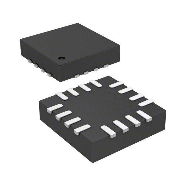
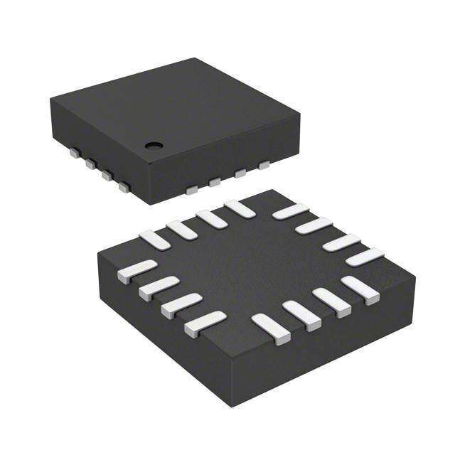
ICGOO电子元器件商城为您提供A3G4250DTR由STMicroelectronics设计生产,在icgoo商城现货销售,并且可以通过原厂、代理商等渠道进行代购。 A3G4250DTR价格参考。STMicroelectronicsA3G4250DTR封装/规格:运动传感器 - 陀螺仪, Gyroscope X (Pitch), Y (Roll), Z (Yaw) ±245 4.45Hz ~ 483Hz I²C, SPI 16-LGA (4x4)。您可以下载A3G4250DTR参考资料、Datasheet数据手册功能说明书,资料中有A3G4250DTR 详细功能的应用电路图电压和使用方法及教程。
STMicroelectronics的A3G4250DTR是一款三轴数字输出陀螺仪,属于运动传感器类别。它广泛应用于多种消费电子和工业领域,具体应用场景包括:

1. 消费电子产品:
   - 智能手机和平板电脑:用于屏幕旋转检测、游戏控制(如体感操作)以及增强现实(AR)应用。
   - 可穿戴设备:如智能手表和健身追踪器,用于步数计算、姿态识别和活动监测。
   - 虚拟现实(VR)头盔:提供头部运动跟踪功能,提升沉浸式体验。

2. 导航与定位:
   - 惯性导航系统:结合加速度计和GPS模块,用于车辆、无人机或机器人中的航向和位置估算。
   - 室内导航:在GPS信号弱的环境中(如建筑物内),通过测量角速度来确定移动方向。

3. 影像稳定:
   - 相机和摄像机:实现光学或电子图像稳定功能,减少拍摄时因手抖产生的模糊现象。
   - 无人机云台:确保摄像头在飞行过程中保持稳定,拍摄清晰画面。

4. 工业自动化:
   - 机器人控制:帮助工业机器人进行精确的姿态调整和动作规划。
   - 机械状态监控:检测振动和不平衡情况,预测设备故障并优化维护计划。

5. 医疗健康:
   - 康复设备:辅助患者完成特定康复训练,记录运动数据以评估恢复进展。
   - 跌倒检测:在老年人护理产品中,快速响应异常姿态变化并触发报警机制。

6. 玩具与娱乐:
   - 遥控车/飞机:提高操控稳定性,使玩家获得更流畅的游戏体验。
   - 互动玩具:支持手势识别功能,增强用户交互乐趣。

A3G4250DTR凭借其低功耗、高灵敏度及紧凑封装特性,在上述领域展现了卓越性能,满足多样化需求。
| 参数 | 数值 |
| 产品目录 | |
| 描述 | IC MEMS MOTION SENSOR 16LGA |
| 产品分类 | 陀螺仪 |
| 品牌 | STMicroelectronics |
| 数据手册 | |
| 产品图片 |
|
| 产品型号 | A3G4250DTR |
| rohs | 无铅 / 符合限制有害物质指令(RoHS)规范要求 |
| 产品系列 | Q 汽车 |
| 供应商器件封装 | 16-LGA(4x4) |
| 其它名称 | 497-13200-1 |
| 其它有关文件 | http://www.st.com/web/catalog/sense_power/FM89/SC1288/PF253244?referrer=70071840 |
| 典型带宽 | 800Hz,400Hz,200Hz,100Hz |
| 封装/外壳 | 16-TFLGA |
| 工作温度 | -40°C ~ 85°C |
| 标准包装 | 1 |
| 灵敏度 | 7.4 mdps/位数 ~ 10.1 mdps/位数 |
| 电压-电源 | 2.4 V ~ 3.6 V |
| 电流-电源 | 7mA |
| 范围°/s | ±245°/s |
| 输出类型 | I²C, SPI |


- 商务部:美国ITC正式对集成电路等产品启动337调查
- 曝三星4nm工艺存在良率问题 高通将骁龙8 Gen1或转产台积电
- 太阳诱电将投资9.5亿元在常州建新厂生产MLCC 预计2023年完工
- 英特尔发布欧洲新工厂建设计划 深化IDM 2.0 战略
- 台积电先进制程称霸业界 有大客户加持明年业绩稳了
- 达到5530亿美元!SIA预计今年全球半导体销售额将创下新高
- 英特尔拟将自动驾驶子公司Mobileye上市 估值或超500亿美元
- 三星加码芯片和SET,合并消费电子和移动部门,撤换高东真等 CEO
- 三星电子宣布重大人事变动 还合并消费电子和移动部门
- 海关总署:前11个月进口集成电路产品价值2.52万亿元 增长14.8%
PDF Datasheet 数据手册内容提取
A3G4250D MEMS motion sensor: 3-axis digital output gyroscope Features ■ Wide supply voltage: 2.4 V to 3.6 V ■ ±245 dps full scale ■ I2C/SPI digital output interface ■ 16-bit rate value data output LGA-16 (4x4x1.1 mm3) ■ 8-bit temperature data output ■ Two digital output lines (interrupt and data ready) ■ Integrated low and high-pass filters with user- Description selectable bandwidth The A3G4250D is a low-power 3-axis angular rate ■ Ultra-stable over temperature and time sensor able to provide unprecedented stability at ■ Low-voltage-compatible IOs (1.8 V) zero rate level and sensitivity over temperature ■ Embedded power-down and sleep mode and time. It includes a sensing element and an IC interface capable of providing the measured ■ Embedded temperature sensor angular rate to the external world through a ■ Embedded FIFO standard SPI digital interface. An I2C-compatible ■ High shock survivability interface is also available. ■ Extended operating temperature range (-40 °C The sensing element is manufactured using a to +85 °C) dedicated micro-machining process developed by ■ ECOPACK® RoHS and “Green” compliant STMicroelectronics to produce inertial sensors and actuators on silicon wafers. ■ AEC-Q100 qualification The IC interface is manufactured using a CMOS process that allows a high level of integration to Applications design a dedicated circuit which is trimmed to better match the sensing element characteristics. ■ In-dash car navigation ■ Telematics, e-Tolling The A3G4250D has a full scale of ±245 dps and is capable of measuring rates with a user- ■ Motion control with MMI (man-machine selectable bandwidth. interface) The A3G4250D is available in a plastic land grid ■ Appliances and robotics array (LGA) package and can operate within a temperature range of -40 °C to +85 °C. Table 1. Device summary Order code Temperature range (°C) Package Packing A3G4250D -40 to +85 LGA-16 (4x4x1.1 mm3) Tray A3G4250DTR -40 to +85 LGA-16 (4x4x1.1 mm3) Tape and reel February 2012 Doc 022768 Rev 3 1/44 www.st.com 44
Contents A3G4250D Contents 1 Block diagram and pin description . . . . . . . . . . . . . . . . . . . . . . . . . . . . . 6 1.1 Pin description . . . . . . . . . . . . . . . . . . . . . . . . . . . . . . . . . . . . . . . . . . . . . . 6 2 Mechanical and electrical characteristics . . . . . . . . . . . . . . . . . . . . . . . . 9 2.1 Mechanical characteristics . . . . . . . . . . . . . . . . . . . . . . . . . . . . . . . . . . . . . 9 2.2 Electrical characteristics . . . . . . . . . . . . . . . . . . . . . . . . . . . . . . . . . . . . . . 10 2.3 Temperature sensor characteristics . . . . . . . . . . . . . . . . . . . . . . . . . . . . . 10 2.4 Communication interface characteristics . . . . . . . . . . . . . . . . . . . . . . . . . 11 2.4.1 SPI - serial peripheral interface . . . . . . . . . . . . . . . . . . . . . . . . . . . . . . . 11 2.4.2 I2C - inter IC control interface . . . . . . . . . . . . . . . . . . . . . . . . . . . . . . . . 12 2.5 Absolute maximum ratings . . . . . . . . . . . . . . . . . . . . . . . . . . . . . . . . . . . . 13 2.6 Terminology . . . . . . . . . . . . . . . . . . . . . . . . . . . . . . . . . . . . . . . . . . . . . . . 14 2.6.1 Sensitivity . . . . . . . . . . . . . . . . . . . . . . . . . . . . . . . . . . . . . . . . . . . . . . . . 14 2.6.2 Zero-rate level . . . . . . . . . . . . . . . . . . . . . . . . . . . . . . . . . . . . . . . . . . . . 14 2.6.3 Stability over temperature and time . . . . . . . . . . . . . . . . . . . . . . . . . . . . 14 2.7 Soldering information . . . . . . . . . . . . . . . . . . . . . . . . . . . . . . . . . . . . . . . . 14 3 Main digital blocks . . . . . . . . . . . . . . . . . . . . . . . . . . . . . . . . . . . . . . . . . 15 3.1 Block diagram . . . . . . . . . . . . . . . . . . . . . . . . . . . . . . . . . . . . . . . . . . . . . . 15 3.2 FIFO . . . . . . . . . . . . . . . . . . . . . . . . . . . . . . . . . . . . . . . . . . . . . . . . . . . . . 15 3.2.1 Bypass mode . . . . . . . . . . . . . . . . . . . . . . . . . . . . . . . . . . . . . . . . . . . . . 15 3.2.2 FIFO mode . . . . . . . . . . . . . . . . . . . . . . . . . . . . . . . . . . . . . . . . . . . . . . . 16 3.2.3 Stream mode . . . . . . . . . . . . . . . . . . . . . . . . . . . . . . . . . . . . . . . . . . . . . 17 3.2.4 Retrieve data from FIFO . . . . . . . . . . . . . . . . . . . . . . . . . . . . . . . . . . . . 18 4 Application hints . . . . . . . . . . . . . . . . . . . . . . . . . . . . . . . . . . . . . . . . . . . 20 5 Digital interfaces . . . . . . . . . . . . . . . . . . . . . . . . . . . . . . . . . . . . . . . . . . . 22 5.1 I2C serial interface . . . . . . . . . . . . . . . . . . . . . . . . . . . . . . . . . . . . . . . . . . 22 5.1.1 I2C operation . . . . . . . . . . . . . . . . . . . . . . . . . . . . . . . . . . . . . . . . . . . . . 23 5.2 SPI bus interface . . . . . . . . . . . . . . . . . . . . . . . . . . . . . . . . . . . . . . . . . . . 24 5.2.1 SPI read . . . . . . . . . . . . . . . . . . . . . . . . . . . . . . . . . . . . . . . . . . . . . . . . . 25 5.2.2 SPI write . . . . . . . . . . . . . . . . . . . . . . . . . . . . . . . . . . . . . . . . . . . . . . . . 26 2/44 Doc 022768 Rev 3
A3G4250D Contents 5.2.3 SPI read in 3-wire mode . . . . . . . . . . . . . . . . . . . . . . . . . . . . . . . . . . . . 27 6 Output register mapping . . . . . . . . . . . . . . . . . . . . . . . . . . . . . . . . . . . . 28 7 Register description . . . . . . . . . . . . . . . . . . . . . . . . . . . . . . . . . . . . . . . . 30 7.1 WHO_AM_I (0Fh) . . . . . . . . . . . . . . . . . . . . . . . . . . . . . . . . . . . . . . . . . . . 30 7.2 CTRL_REG1 (20h) . . . . . . . . . . . . . . . . . . . . . . . . . . . . . . . . . . . . . . . . . . 30 7.3 CTRL_REG2 (21h) . . . . . . . . . . . . . . . . . . . . . . . . . . . . . . . . . . . . . . . . . . 31 7.4 CTRL_REG3 (22h) . . . . . . . . . . . . . . . . . . . . . . . . . . . . . . . . . . . . . . . . . . 32 7.5 CTRL_REG4 (23h) . . . . . . . . . . . . . . . . . . . . . . . . . . . . . . . . . . . . . . . . . . 33 7.6 CTRL_REG5 (24h) . . . . . . . . . . . . . . . . . . . . . . . . . . . . . . . . . . . . . . . . . . 33 7.7 REFERENCE/DATACAPTURE (25h) . . . . . . . . . . . . . . . . . . . . . . . . . . . . 35 7.8 OUT_TEMP (26h) . . . . . . . . . . . . . . . . . . . . . . . . . . . . . . . . . . . . . . . . . . 35 7.9 STATUS_REG (27h) . . . . . . . . . . . . . . . . . . . . . . . . . . . . . . . . . . . . . . . . . 35 7.10 OUT_X_L (28h), OUT_X_H (29h) . . . . . . . . . . . . . . . . . . . . . . . . . . . . . . 36 7.11 OUT_Y_L (2Ah), OUT_Y_H (2Bh) . . . . . . . . . . . . . . . . . . . . . . . . . . . . . . 36 7.12 OUT_Z_L (2Ch), OUT_Z_H (2Dh) . . . . . . . . . . . . . . . . . . . . . . . . . . . . . . 36 7.13 FIFO_CTRL_REG (2Eh) . . . . . . . . . . . . . . . . . . . . . . . . . . . . . . . . . . . . . 36 7.14 FIFO_SRC_REG (2Fh) . . . . . . . . . . . . . . . . . . . . . . . . . . . . . . . . . . . . . . 36 7.15 INT1_CFG (30h) . . . . . . . . . . . . . . . . . . . . . . . . . . . . . . . . . . . . . . . . . . . . 37 7.16 INT1_SRC (31h) . . . . . . . . . . . . . . . . . . . . . . . . . . . . . . . . . . . . . . . . . . . . 37 7.17 INT1_THS_XH (32h) . . . . . . . . . . . . . . . . . . . . . . . . . . . . . . . . . . . . . . . . 38 7.18 INT1_THS_XL (33h) . . . . . . . . . . . . . . . . . . . . . . . . . . . . . . . . . . . . . . . . . 38 7.19 INT1_THS_YH (34h) . . . . . . . . . . . . . . . . . . . . . . . . . . . . . . . . . . . . . . . . 38 7.20 INT1_THS_YL (35h) . . . . . . . . . . . . . . . . . . . . . . . . . . . . . . . . . . . . . . . . . 39 7.21 INT1_THS_ZH (36h) . . . . . . . . . . . . . . . . . . . . . . . . . . . . . . . . . . . . . . . . 39 7.22 INT1_THS_ZL (37h) . . . . . . . . . . . . . . . . . . . . . . . . . . . . . . . . . . . . . . . . . 39 7.23 INT1_DURATION (38h) . . . . . . . . . . . . . . . . . . . . . . . . . . . . . . . . . . . . . . 39 8 Package information . . . . . . . . . . . . . . . . . . . . . . . . . . . . . . . . . . . . . . . . 41 9 Revision history . . . . . . . . . . . . . . . . . . . . . . . . . . . . . . . . . . . . . . . . . . . 42 Doc 022768 Rev 3 3/44
List of tables A3G4250D List of tables Table 1. Device summary. . . . . . . . . . . . . . . . . . . . . . . . . . . . . . . . . . . . . . . . . . . . . . . . . . . . . . . . . . 1 Table 2. Pin description . . . . . . . . . . . . . . . . . . . . . . . . . . . . . . . . . . . . . . . . . . . . . . . . . . . . . . . . . . . 6 Table 3. Filter values . . . . . . . . . . . . . . . . . . . . . . . . . . . . . . . . . . . . . . . . . . . . . . . . . . . . . . . . . . . . . 7 Table 4. Mechanical characteristics . . . . . . . . . . . . . . . . . . . . . . . . . . . . . . . . . . . . . . . . . . . . . . . . . . 8 Table 5. Electrical characteristics. . . . . . . . . . . . . . . . . . . . . . . . . . . . . . . . . . . . . . . . . . . . . . . . . . . . 9 Table 6. Temp. sensor characteristics . . . . . . . . . . . . . . . . . . . . . . . . . . . . . . . . . . . . . . . . . . . . . . . . 9 Table 7. SPI slave timing values. . . . . . . . . . . . . . . . . . . . . . . . . . . . . . . . . . . . . . . . . . . . . . . . . . . . 10 Table 8. I2C slave timing values. . . . . . . . . . . . . . . . . . . . . . . . . . . . . . . . . . . . . . . . . . . . . . . . . . . . 11 Table 9. Absolute maximum ratings. . . . . . . . . . . . . . . . . . . . . . . . . . . . . . . . . . . . . . . . . . . . . . . . . 12 Table 10. PLL low-pass filter component values . . . . . . . . . . . . . . . . . . . . . . . . . . . . . . . . . . . . . . . . 19 Table 11. Serial interface pin description . . . . . . . . . . . . . . . . . . . . . . . . . . . . . . . . . . . . . . . . . . . . . . 21 Table 12. I2C terminology. . . . . . . . . . . . . . . . . . . . . . . . . . . . . . . . . . . . . . . . . . . . . . . . . . . . . . . . . . 21 Table 13. SAD+read/write patterns. . . . . . . . . . . . . . . . . . . . . . . . . . . . . . . . . . . . . . . . . . . . . . . . . . . 22 Table 14. Transfer when master is writing one byte to slave . . . . . . . . . . . . . . . . . . . . . . . . . . . . . . . 22 Table 15. Transfer when master is writing multiple bytes to slave . . . . . . . . . . . . . . . . . . . . . . . . . . . 23 Table 16. Transfer when master is receiving (reading) one byte of data from slave . . . . . . . . . . . . . 23 Table 17. Transfer when master is receiving (reading) multiple bytes of data from slave . . . . . . . . . 23 Table 18. Register address map. . . . . . . . . . . . . . . . . . . . . . . . . . . . . . . . . . . . . . . . . . . . . . . . . . . . . 27 Table 19. WHO_AM_I register . . . . . . . . . . . . . . . . . . . . . . . . . . . . . . . . . . . . . . . . . . . . . . . . . . . . . . 29 Table 20. CTRL_REG1 register . . . . . . . . . . . . . . . . . . . . . . . . . . . . . . . . . . . . . . . . . . . . . . . . . . . . . 29 Table 21. CTRL_REG1 description . . . . . . . . . . . . . . . . . . . . . . . . . . . . . . . . . . . . . . . . . . . . . . . . . . 29 Table 22. DR and BW configuration setting . . . . . . . . . . . . . . . . . . . . . . . . . . . . . . . . . . . . . . . . . . . . 29 Table 23. Power mode selection configuration. . . . . . . . . . . . . . . . . . . . . . . . . . . . . . . . . . . . . . . . . . 30 Table 24. CTRL_REG2 register . . . . . . . . . . . . . . . . . . . . . . . . . . . . . . . . . . . . . . . . . . . . . . . . . . . . . 30 Table 25. CTRL_REG2 description . . . . . . . . . . . . . . . . . . . . . . . . . . . . . . . . . . . . . . . . . . . . . . . . . . 30 Table 26. High-pass filter mode configuration . . . . . . . . . . . . . . . . . . . . . . . . . . . . . . . . . . . . . . . . . . 31 Table 27. High-pass filter cut-off frequency configuration [Hz]. . . . . . . . . . . . . . . . . . . . . . . . . . . . . . 31 Table 28. CTRL_REG1 register . . . . . . . . . . . . . . . . . . . . . . . . . . . . . . . . . . . . . . . . . . . . . . . . . . . . . 31 Table 29. CTRL_REG3 description . . . . . . . . . . . . . . . . . . . . . . . . . . . . . . . . . . . . . . . . . . . . . . . . . . 31 Table 30. CTRL_REG4 register . . . . . . . . . . . . . . . . . . . . . . . . . . . . . . . . . . . . . . . . . . . . . . . . . . . . . 32 Table 31. CTRL_REG4 description . . . . . . . . . . . . . . . . . . . . . . . . . . . . . . . . . . . . . . . . . . . . . . . . . . 32 Table 32. Self-test mode configuration. . . . . . . . . . . . . . . . . . . . . . . . . . . . . . . . . . . . . . . . . . . . . . . . 32 Table 33. CTRL_REG5 register . . . . . . . . . . . . . . . . . . . . . . . . . . . . . . . . . . . . . . . . . . . . . . . . . . . . . 32 Table 34. CTRL_REG5 description . . . . . . . . . . . . . . . . . . . . . . . . . . . . . . . . . . . . . . . . . . . . . . . . . . 32 Table 35. Out_Sel configuration settings . . . . . . . . . . . . . . . . . . . . . . . . . . . . . . . . . . . . . . . . . . . . . . 33 Table 36. INT_SEL configuration settings . . . . . . . . . . . . . . . . . . . . . . . . . . . . . . . . . . . . . . . . . . . . . 33 Table 37. REFERENCE register. . . . . . . . . . . . . . . . . . . . . . . . . . . . . . . . . . . . . . . . . . . . . . . . . . . . . 34 Table 38. REFERENCE register description . . . . . . . . . . . . . . . . . . . . . . . . . . . . . . . . . . . . . . . . . . . 34 Table 39. OUT_TEMP register. . . . . . . . . . . . . . . . . . . . . . . . . . . . . . . . . . . . . . . . . . . . . . . . . . . . . . 34 Table 40. OUT_TEMP register description. . . . . . . . . . . . . . . . . . . . . . . . . . . . . . . . . . . . . . . . . . . . . 34 Table 41. STATUS_REG register. . . . . . . . . . . . . . . . . . . . . . . . . . . . . . . . . . . . . . . . . . . . . . . . . . . . 34 Table 42. STATUS_REG description. . . . . . . . . . . . . . . . . . . . . . . . . . . . . . . . . . . . . . . . . . . . . . . . . 34 Table 43. REFERENCE register. . . . . . . . . . . . . . . . . . . . . . . . . . . . . . . . . . . . . . . . . . . . . . . . . . . . . 35 Table 44. REFERENCE register description . . . . . . . . . . . . . . . . . . . . . . . . . . . . . . . . . . . . . . . . . . . 35 Table 45. FIFO mode configuration . . . . . . . . . . . . . . . . . . . . . . . . . . . . . . . . . . . . . . . . . . . . . . . . . . 35 Table 46. FIFO_SRC register. . . . . . . . . . . . . . . . . . . . . . . . . . . . . . . . . . . . . . . . . . . . . . . . . . . . . . . 35 Table 47. FIFO_SRC register description. . . . . . . . . . . . . . . . . . . . . . . . . . . . . . . . . . . . . . . . . . . . . . 35 Table 48. INT1_CFG register. . . . . . . . . . . . . . . . . . . . . . . . . . . . . . . . . . . . . . . . . . . . . . . . . . . . . . . 36 4/44 Doc 022768 Rev 3
A3G4250D List of tables Table 49. INT1_CFG description . . . . . . . . . . . . . . . . . . . . . . . . . . . . . . . . . . . . . . . . . . . . . . . . . . . . 36 Table 50. INT1_SRC register. . . . . . . . . . . . . . . . . . . . . . . . . . . . . . . . . . . . . . . . . . . . . . . . . . . . . . . 36 Table 51. INT1_SRC description . . . . . . . . . . . . . . . . . . . . . . . . . . . . . . . . . . . . . . . . . . . . . . . . . . . . 37 Table 52. INT1_THS_XH register. . . . . . . . . . . . . . . . . . . . . . . . . . . . . . . . . . . . . . . . . . . . . . . . . . . . 37 Table 53. INT1_THS_XH description. . . . . . . . . . . . . . . . . . . . . . . . . . . . . . . . . . . . . . . . . . . . . . . . . 37 Table 54. INT1_THS_XL register. . . . . . . . . . . . . . . . . . . . . . . . . . . . . . . . . . . . . . . . . . . . . . . . . . . . 37 Table 55. INT1_THS_XL description . . . . . . . . . . . . . . . . . . . . . . . . . . . . . . . . . . . . . . . . . . . . . . . . . 37 Table 56. INT1_THS_YH register. . . . . . . . . . . . . . . . . . . . . . . . . . . . . . . . . . . . . . . . . . . . . . . . . . . . 37 Table 57. INT1_THS_YH description. . . . . . . . . . . . . . . . . . . . . . . . . . . . . . . . . . . . . . . . . . . . . . . . . 37 Table 58. INT1_THS_YL register. . . . . . . . . . . . . . . . . . . . . . . . . . . . . . . . . . . . . . . . . . . . . . . . . . . . 38 Table 59. INT1_THS_YL description . . . . . . . . . . . . . . . . . . . . . . . . . . . . . . . . . . . . . . . . . . . . . . . . . 38 Table 60. INT1_THS_ZH register. . . . . . . . . . . . . . . . . . . . . . . . . . . . . . . . . . . . . . . . . . . . . . . . . . . . 38 Table 61. INT1_THS_ZH description . . . . . . . . . . . . . . . . . . . . . . . . . . . . . . . . . . . . . . . . . . . . . . . . . 38 Table 62. INT1_THS_ZL register . . . . . . . . . . . . . . . . . . . . . . . . . . . . . . . . . . . . . . . . . . . . . . . . . . . . 38 Table 63. INT1_THS_ZL description . . . . . . . . . . . . . . . . . . . . . . . . . . . . . . . . . . . . . . . . . . . . . . . . . 38 Table 64. INT1_DURATION register . . . . . . . . . . . . . . . . . . . . . . . . . . . . . . . . . . . . . . . . . . . . . . . . . 38 Table 65. INT1_DURATION description. . . . . . . . . . . . . . . . . . . . . . . . . . . . . . . . . . . . . . . . . . . . . . . 38 Table 66. Document revision history . . . . . . . . . . . . . . . . . . . . . . . . . . . . . . . . . . . . . . . . . . . . . . . . . 41 Doc 022768 Rev 3 5/44
List of figures A3G4250D List of figures Figure 1. Block diagram. . . . . . . . . . . . . . . . . . . . . . . . . . . . . . . . . . . . . . . . . . . . . . . . . . . . . . . . . . . . 5 Figure 2. Pin connection . . . . . . . . . . . . . . . . . . . . . . . . . . . . . . . . . . . . . . . . . . . . . . . . . . . . . . . . . . . 5 Figure 3. A3G4250D external low-pass filter values . . . . . . . . . . . . . . . . . . . . . . . . . . . . . . . . . . . . . . 6 Figure 4. SPI slave timing diagram . . . . . . . . . . . . . . . . . . . . . . . . . . . . . . . . . . . . . . . . . . . . . . . . . . 10 Figure 5. I2C slave timing diagram . . . . . . . . . . . . . . . . . . . . . . . . . . . . . . . . . . . . . . . . . . . . . . . . . . 11 Figure 6. Block diagram. . . . . . . . . . . . . . . . . . . . . . . . . . . . . . . . . . . . . . . . . . . . . . . . . . . . . . . . . . . 14 Figure 7. Bypass mode . . . . . . . . . . . . . . . . . . . . . . . . . . . . . . . . . . . . . . . . . . . . . . . . . . . . . . . . . . . 15 Figure 8. FIFO mode . . . . . . . . . . . . . . . . . . . . . . . . . . . . . . . . . . . . . . . . . . . . . . . . . . . . . . . . . . . . . 16 Figure 9. Stream mode . . . . . . . . . . . . . . . . . . . . . . . . . . . . . . . . . . . . . . . . . . . . . . . . . . . . . . . . . . . 17 Figure 10. FIFO access sequence in asynchronous mode . . . . . . . . . . . . . . . . . . . . . . . . . . . . . . . . . 18 Figure 11. A3G4250D electrical connections and external component values . . . . . . . . . . . . . . . . . . 19 Figure 12. Read and write protocol . . . . . . . . . . . . . . . . . . . . . . . . . . . . . . . . . . . . . . . . . . . . . . . . . . . 24 Figure 13. SPI read protocol . . . . . . . . . . . . . . . . . . . . . . . . . . . . . . . . . . . . . . . . . . . . . . . . . . . . . . . . 24 Figure 14. Multiple byte SPI read protocol (2-byte example). . . . . . . . . . . . . . . . . . . . . . . . . . . . . . . . 25 Figure 15. SPI write protocol . . . . . . . . . . . . . . . . . . . . . . . . . . . . . . . . . . . . . . . . . . . . . . . . . . . . . . . . 25 Figure 16. Multiple byte SPI write protocol (2-byte example). . . . . . . . . . . . . . . . . . . . . . . . . . . . . . . . 26 Figure 17. SPI read protocol in 3-wire mode. . . . . . . . . . . . . . . . . . . . . . . . . . . . . . . . . . . . . . . . . . . . 26 Figure 18. INT1_Sel and Out_Sel configuration block diagram. . . . . . . . . . . . . . . . . . . . . . . . . . . . . . 33 Figure 19. Wait disabled . . . . . . . . . . . . . . . . . . . . . . . . . . . . . . . . . . . . . . . . . . . . . . . . . . . . . . . . . . . 39 Figure 20. Wait enabled. . . . . . . . . . . . . . . . . . . . . . . . . . . . . . . . . . . . . . . . . . . . . . . . . . . . . . . . . . . . 39 Figure 21. LGA-16: mechanical data and package dimensions . . . . . . . . . . . . . . . . . . . . . . . . . . . . . 40 6/44 Doc 022768 Rev 3
A3G4250D Block diagram and pin description 1 Block diagram and pin description Figure 1. Block diagram Ω + x,y,z X+ CHARGE MIXER LOW-PASS YZYZ+-+- MUX AMP FILTER DCA1 LGDATII RNEFTLII SI2PCI CSSSDCDSLOA//SSPDCO/SDI X- G T E M P S E E A DRIVING MASS RA NS DC T O 2 U R Feedback loop R E CLOCK CONTROL LOGIC INT1 TRIMMING REFERENCE FIFO & & CIRCUITS PHASE GENERATOR INTERRUPT GEN. DRDY/INT2 AM07225v1 The vibration of the structure is maintained by drive circuitry in a feedback loop. The sensing signal is filtered and appears as a digital signal at the output. 1.1 Pin description Figure 2. Pin connection +Ω P Z L L G F R V N IL E d D T S d 1 X 13 16 +Ω Y RES 12 1 Vdd_IO RES BOTTOM SCL/SPC VIEW RES SDA/SDI/SDO +Ω RES 9 4 SDO/SA0 X 8 5 (TOP VIEW) R IN D C E R S T DIRECTIONS OF THE S D Y DETECTABLE / I ANGULAR RATES N T 2 AM07226v1 Doc 022768 Rev 3 7/44
Block diagram and pin description A3G4250D Table 2. Pin description Pin# Name Function 1 Vdd_IO Power supply for I/O pins SCL I2C serial clock (SCL) 2 SPC SPI serial port clock (SPC) SDA I2C serial data (SDA) 3 SDI SPI serial data input (SDI) SDO 3-wire interface serial data output (SDO) SDO SPI serial data output (SDO) 4 SA0 I2C least significant bit of the device address (SA0) SPI enable 5 CS I2C/SPI mode selection (1: SPI idle mode / I2C communication enabled; 0: SPI communication mode / I2C disabled) 6 DRDY/INT2 Data ready/FIFO interrupt 7 INT1 Programmable interrupt 8 Reserved Connect to GND 9 Reserved Connect to GND 10 Reserved Connect to GND 11 Reserved Connect to GND 12 Reserved Connect to GND 13 GND 0 V supply 14 PLLFILT Phase-locked loop filter (see Figure3) 15 Reserved Connect to Vdd 16 Vdd Power supply Figure 3. A3G4250D external low-pass filter values(a) (cid:35)(cid:65)(cid:80)(cid:65)(cid:67)(cid:73)(cid:84)(cid:79)(cid:82)(cid:0)(cid:70)(cid:79)(cid:82)(cid:0) (cid:44)(cid:79)(cid:87)(cid:13)(cid:80)(cid:65)(cid:83)(cid:83)(cid:0)(cid:70)(cid:73)(cid:76)(cid:84)(cid:69)(cid:82) (cid:84)(cid:79)(cid:0)(cid:80)(cid:73)(cid:78)(cid:0)(cid:17)(cid:20) (cid:35)(cid:17) (cid:35)(cid:18) (cid:50)(cid:18) (cid:39)(cid:46)(cid:36) (cid:33)(cid:45)(cid:16)(cid:23)(cid:18)(cid:18)(cid:23)(cid:86)(cid:17) a. Pin 14 PLLFILT maximum voltage level is equal to Vdd. 8/44 Doc 022768 Rev 3
A3G4250D Block diagram and pin description Table 3. Filter values Parameter Typical value C1 10 nF C2 470 nF R2 10 kΩ Doc 022768 Rev 3 9/44
Mechanical and electrical characteristics A3G4250D 2 Mechanical and electrical characteristics 2.1 Mechanical characteristics @ Vdd = 3.0 V, T = -40... +85 °C, unless otherwise noted(b). Table 4. M echanical characteristics Symbol Parameter Test condition Min. Typ.(1) Max. Unit FS Measurement range(2) ±245 dps So Sensitivity(3) 7.4 8.75 10.1 mdps/digit Sensitivity change vs. SoDr ±2 % temperature DVoff Digital zero-rate level(3) -25 +25 dps Zero-rate level change OffDr ±0.03 dps/°C vs. temperature NL Non linearity(2) Best fit straight line -5 0.2 +5 % FS DST Self-test output change 55 130 245 dps dps/ Rn Rate noise density BW = 50 Hz 0.03 0.15 sqrt(Hz) 89/176/ 105/208/ 121/239/ ODR Digital output data rate Hz 357/714 420/840 483/966 Operating temperature Top -40 +85 °C range 1. Typical specifications are not guaranteed; typical values at +25 °C. 2. Guaranteed by design. 3. Across temperature and after MSL3 preconditioning. b. The product is factory calibrated at 3.0 V. The operational power supply range is specified in Table5. 10/44 Doc 022768 Rev 3
A3G4250D Mechanical and electrical characteristics 2.2 Electrical characteristics @ Vdd = 3.0 V, T = -40... +85 °C, unless otherwise noted(c). Table 5. Electrical characteristics Symbol Parameter Test condition Min. Typ.(1) Max. Unit Vdd Supply voltage 2.4 3.0 3.6 V Vdd_IO I/O pins supply voltage(2) 1.71 Vdd+0.1 V Idd Supply current 4.8 6.1 7.0 mA Supply current Selectable by digital IddSL 1.5 mA in sleep mode(3) interface Supply current in Selectable by digital IddPdn 5 10 µA power-down mode(4) interface Operating temperature Top -40 +85 °C range 1. Typical specifications are not guaranteed; typical values at +25 °C. 2. It is possible to remove Vdd maintaining Vdd_IO without blocking the communication busses, in this condition the measurement chain is powered off. 3. Sleep mode introduces a faster turn-on time compared to power-down mode. 4. Verified at wafer level. 2.3 Temperature sensor characteristics @ Vdd = 3.0 V, T = 25 °C, unless otherwise noted(d). Table 6. Temp. sensor characteristics Symbol Parameter Test condition Min. Typ.(1) Max. Unit Temperature sensor TSDr output change vs. -1 °C/digit temperature - TODR Temperature refresh rate 1 Hz Operating temperature Top -40 +85 °C range 1. Typical specifications are not guaranteed; typical values at +25 °C. c. The product is factory calibrated at 3.0 V. d. The product is factory calibrated at 3.0 V. Doc 022768 Rev 3 11/44
Mechanical and electrical characteristics A3G4250D 2.4 Communication interface characteristics 2.4.1 SPI - serial peripheral interface Subject to general operating conditions for Vdd and Top. Table 7. SPI slave timing values Value(1) Symbol Parameter Unit Min. Max. tc(SPC) SPI clock cycle 100 ns fc(SPC) SPI clock frequency 10 MHz tsu(CS) CS setup time 5 th(CS) CS hold time 8 tsu(SI) SDI input setup time 5 th(SI) SDI input hold time 15 ns tv(SO) SDO valid output time 50 th(SO) SDO output hold time 6 tdis(SO) SDO output disable time 50 1. Values are guaranteed at 10 MHz clock frequency for SPI with both 4 and 3 wires, based on characterization results; not tested in production. Figure 4. SPI slave timing diagram(e) (cid:38)(cid:54)(cid:3) (cid:8)(cid:19)(cid:9)(cid:0) (cid:8)(cid:19)(cid:9) (cid:87)(cid:86)(cid:88)(cid:11)(cid:38)(cid:54)(cid:12) (cid:87)(cid:70)(cid:11)(cid:54)(cid:51)(cid:38)(cid:12) (cid:87)(cid:75)(cid:11)(cid:38)(cid:54)(cid:12) (cid:54)(cid:51)(cid:38)(cid:3) (cid:8)(cid:19)(cid:9)(cid:0) (cid:8)(cid:19)(cid:9) (cid:87) (cid:87) (cid:86)(cid:88)(cid:11)(cid:54)(cid:44)(cid:12) (cid:75)(cid:11)(cid:54)(cid:44)(cid:12) (cid:54)(cid:39)(cid:44)(cid:3) (cid:8)(cid:19)(cid:9)(cid:0) (cid:48)(cid:54)(cid:37)(cid:3)(cid:44)(cid:49)(cid:3) (cid:47)(cid:54)(cid:37)(cid:3)(cid:44)(cid:49)(cid:3) (cid:8)(cid:19)(cid:9) (cid:87)(cid:89)(cid:11)(cid:54)(cid:50)(cid:12) (cid:87)(cid:75)(cid:11)(cid:54)(cid:50)(cid:12) (cid:87)(cid:71)(cid:76)(cid:86)(cid:11)(cid:54)(cid:50)(cid:12) (cid:54)(cid:39)(cid:50)(cid:3) (cid:8)(cid:19)(cid:9)(cid:0) (cid:48)(cid:54)(cid:37)(cid:3)(cid:50)(cid:56)(cid:55)(cid:3) (cid:47)(cid:54)(cid:37)(cid:3)(cid:50)(cid:56)(cid:55)(cid:3) (cid:8)(cid:19)(cid:9) (cid:33)(cid:45)(cid:16)(cid:23)(cid:18)(cid:18)(cid:24)(cid:86)(cid:17) e. Measurement points are done at 0.2·Vdd_IO and 0.8·Vdd_IO, for both input and output ports. 12/44 Doc 022768 Rev 3
A3G4250D Mechanical and electrical characteristics 2.4.2 I2C - inter IC control interface Subject to general operating conditions for Vdd and Top. Table 8. I2C slave timing values I2C standard mode(1) I2C fast mode(1) Symbol Parameter Unit Min. Max. Min. Max. f(SCL) SCL clock frequency 0 100 0 400 kHz tw(SCLL) SCL clock low time 4.7 1.3 µs tw(SCLH) SCL clock high time 4.0 0.6 tsu(SDA) SDA setup time 250 100 ns th(SDA) SDA data hold time 0 3.45 0 0.9 µs th(ST) START condition hold time 4 0.6 Repeated START condition tsu(SR) setup time 4.7 0.6 µs tsu(SP) STOP condition setup time 4 0.6 Bus free time between STOP tw(SP:SR) and START condition 4.7 1.3 1. Data based on standard I2C protocol requirement; not tested in production. Figure 5. I2C slave timing diagram(f) (cid:53)(cid:40)(cid:51)(cid:40)(cid:36)(cid:55)(cid:40)(cid:39) (cid:54)(cid:55)(cid:36)(cid:53)(cid:55)(cid:3) (cid:54)(cid:55)(cid:36)(cid:53)(cid:55)(cid:3) (cid:87) (cid:86)(cid:88)(cid:11)(cid:54)(cid:53)(cid:12) (cid:87) (cid:54)(cid:55)(cid:36)(cid:53)(cid:55) (cid:54)(cid:39)(cid:36)(cid:3) (cid:90)(cid:11)(cid:54)(cid:51)(cid:29)(cid:54)(cid:53)(cid:12) (cid:87)(cid:73)(cid:11)(cid:54)(cid:39)(cid:36)(cid:12) (cid:87)(cid:85)(cid:11)(cid:54)(cid:39)(cid:36)(cid:12) (cid:87)(cid:86)(cid:88)(cid:11)(cid:54)(cid:39)(cid:36)(cid:12) (cid:87)(cid:75)(cid:11)(cid:54)(cid:39)(cid:36)(cid:12) (cid:87) (cid:54)(cid:55)(cid:50)(cid:51) (cid:86)(cid:88)(cid:11)(cid:54)(cid:51)(cid:12) (cid:54)(cid:38)(cid:47)(cid:3) (cid:87) (cid:87) (cid:87) (cid:87) (cid:87) (cid:33)(cid:45)(cid:16)(cid:23)(cid:18)(cid:18)(cid:25)(cid:86)(cid:17) (cid:75)(cid:11)(cid:54)(cid:55)(cid:12) (cid:90)(cid:11)(cid:54)(cid:38)(cid:47)(cid:47)(cid:12) (cid:90)(cid:11)(cid:54)(cid:38)(cid:47)(cid:43)(cid:12) (cid:85)(cid:11)(cid:54)(cid:38)(cid:47)(cid:12) (cid:73)(cid:11)(cid:54)(cid:38)(cid:47)(cid:12) f. Measurement points are done at 0.2·Vdd_IO and 0.8·Vdd_IO, for both ports. Doc 022768 Rev 3 13/44
Mechanical and electrical characteristics A3G4250D 2.5 Absolute maximum ratings Any stress above that listed as “Absolute maximum ratings” may cause permanent damage to the device. This is a stress rating only and functional operation of the device under these conditions is not implied. Exposure to maximum rating conditions for extended periods may affect device reliability. Table 9. Absolute maximum ratings Symbol Ratings Maximum value Unit Vdd Supply voltage -0.3 to 4.8 V T Storage temperature range -40 to +125 °C STG Sg Acceleration g for 0.1 ms 10,000 g ESD Electrostatic discharge protection 2 (HBM) kV This is a mechanical shock sensitive device, improper handling can cause permanent damage to the part This is an ESD sensitive device, improper handling can cause permanent damage to the part 14/44 Doc 022768 Rev 3
A3G4250D Mechanical and electrical characteristics 2.6 Terminology 2.6.1 Sensitivity An angular rate gyroscope is a device that produces a positive-going digital output for counter-clockwise rotation around the sensitive axis considered. Sensitivity describes the gain of the sensor and can be determined by applying a defined angular velocity to it. This value changes very little over temperature and time. 2.6.2 Zero-rate level The zero-rate level describes the actual output signal if there is no angular rate present. The zero-rate level of precise MEMS sensors is, to some extent, a result of stress to the sensor and, therefore, the zero-rate level can slightly change after mounting the sensor onto a printed circuit board or after exposing it to extensive mechanical stress. This value changes very little over temperature and time. 2.6.3 Stability over temperature and time Thanks to the unique single-driving mass approach and optimized design, ST gyroscopes are able to guarantee a perfect match of the MEMS mechanical mass and the ASIC interface, and deliver unprecedented levels of stability over temperature and time. With the zero-rate level and sensitivity performances, up to ten times better than equivalent products currently available on the market, the A3G4250D allows the user to avoid any further compensation and calibration during production for a faster time to market, easy application implementation, higher performance, and cost saving. 2.7 Soldering information The LGA package is compliant with the ECOPACK®, RoHS and “Green” standard. It is qualified for soldering heat resistance according to JEDEC J-STD-020. Leave “pin 1 indicator” unconnected during soldering. Land pattern and soldering recommendations are available at www.st.com/. Doc 022768 Rev 3 15/44
Main digital blocks A3G4250D 3 Main digital blocks 3.1 Block diagram Figure 6. Block diagram (cid:47)(cid:85)(cid:84)(cid:63)(cid:51)(cid:69)(cid:76) (cid:16)(cid:16)(cid:0) (cid:16)(cid:17)(cid:0) (cid:36)(cid:65)(cid:84)(cid:65)(cid:50)(cid:69)(cid:71) (cid:16) (cid:38)(cid:41)(cid:38)(cid:47) (cid:17)(cid:16)(cid:0) (cid:44)(cid:48)(cid:38)(cid:18) (cid:19)(cid:18)(cid:88)(cid:17)(cid:22)(cid:88)(cid:19) (cid:17)(cid:17) (cid:33)(cid:36)(cid:35) (cid:44)(cid:48)(cid:38)(cid:17) (cid:40)(cid:48)(cid:38) (cid:17) (cid:41)(cid:18)(cid:35) (cid:51)(cid:48)(cid:41) (cid:40)(cid:48)(cid:69)(cid:78) (cid:41)(cid:46)(cid:52)(cid:63)(cid:51)(cid:69)(cid:76) (cid:17)(cid:16)(cid:0) (cid:17)(cid:17)(cid:0) (cid:41)(cid:78)(cid:84)(cid:69)(cid:82)(cid:82)(cid:85)(cid:80)(cid:84)(cid:0) (cid:16)(cid:17)(cid:0) (cid:71)(cid:69)(cid:78)(cid:69)(cid:82)(cid:65)(cid:84)(cid:79)(cid:82) (cid:16)(cid:16)(cid:0) (cid:51)(cid:35)(cid:50)(cid:0)(cid:50)(cid:37)(cid:39) (cid:35)(cid:47)(cid:46)(cid:38)(cid:0)(cid:50)(cid:37)(cid:39) (cid:41)(cid:46)(cid:52)(cid:17) (cid:33)(cid:45)(cid:16)(cid:23)(cid:18)(cid:19)(cid:16)(cid:86)(cid:17) 3.2 FIFO The A3G4250D embeds a 32-slot, 16-bit data FIFO for each of the three output channels: yaw, pitch, and roll. This allows consistent power saving for the system, as the host processor does not need to continuously poll data from the sensor. Instead, it can wake up only when needed and burst the significant data out from the FIFO. This buffer can work in five different modes. Each mode is selected by the FIFO_MODE bits in FIFO_CTRL_REG. Programmable watermark level, FIFO_empty or FIFO_Full events can be enabled to generate dedicated interrupts on the DRDY/INT2 pin (configured through CTRL_REG3), and event detection information is available in FIFO_SRC_REG. The watermark level can be configured to WTM4: 0 in FIFO_CTRL_REG. 3.2.1 Bypass mode In bypass mode, the FIFO is not operational and for this reason it remains empty. As illustrated in Figure7, only the first address is used for each channel. The remaining FIFO slots are empty. When new data is available, the old data is overwritten. 16/44 Doc 022768 Rev 3
A3G4250D Main digital blocks Figure 7. Bypass mode (cid:88)(cid:12)(cid:89)(cid:12)(cid:90) (cid:73) (cid:73) (cid:73) (cid:88) (cid:89)(cid:89) (cid:90) (cid:16) (cid:73)(cid:16) (cid:16) (cid:88) (cid:89) (cid:90) (cid:17) (cid:17) (cid:17) (cid:88) (cid:89) (cid:90) (cid:69)(cid:77)(cid:80)(cid:84)(cid:89) (cid:18) (cid:18) (cid:18) (cid:88) (cid:89) (cid:90) (cid:19)(cid:17) (cid:19)(cid:17) (cid:19)(cid:17) (cid:33)(cid:45)(cid:16)(cid:23)(cid:18)(cid:19)(cid:17)(cid:86)(cid:17) 3.2.2 FIFO mode In FIFO mode, data from the yaw, pitch, and roll channels are stored in the FIFO. A watermark interrupt can be enabled (I2_WMK bit in CTRL_REG3), which is triggered when the FIFO is filled to the level specified in the WTM 4: 0 bits of FIFO_CTRL_REG. The FIFO continues filling until it is full (32 slots of 16-bit data for yaw, pitch, and roll). When full, the FIFO stops collecting data from the input channels. To restart data collection, it is necessary to write FIFO_CTRL_REG back to bypass mode. FIFO mode is represented in Figure8. Doc 022768 Rev 3 17/44
Main digital blocks A3G4250D Figure 8. FIFO mode (cid:88)(cid:12)(cid:89)(cid:12)(cid:90) (cid:73) (cid:73) (cid:73) (cid:88) (cid:89)(cid:89) (cid:90) (cid:16) (cid:73)(cid:16) (cid:16) (cid:88) (cid:89) (cid:90) (cid:17) (cid:17) (cid:17) (cid:88) (cid:89) (cid:90) (cid:18) (cid:18) (cid:18) (cid:88) (cid:89) (cid:90) (cid:19)(cid:17) (cid:19)(cid:17) (cid:19)(cid:17) (cid:33)(cid:45)(cid:16)(cid:23)(cid:18)(cid:19)(cid:18)(cid:86)(cid:17) 3.2.3 Stream mode In stream mode, data from yaw, pitch, and roll measurements are stored in the FIFO. A watermark interrupt can be enabled and set as in FIFO mode. The FIFO continues filling until full (32 slots of 16-bit data for yaw, pitch, and roll). When full, the FIFO discards the older data as the new data arrives. Programmable watermark level events can be enabled to generate dedicated interrupts on the DRDY/INT2 pin (configured through CTRL_REG3). Stream mode is represented in Figure9. 18/44 Doc 022768 Rev 3
A3G4250D Main digital blocks Figure 9. Stream mode (cid:88)(cid:12)(cid:89)(cid:12)(cid:90) (cid:73) (cid:73) (cid:73) (cid:88) (cid:89) (cid:90) (cid:16) (cid:16) (cid:16) (cid:88) (cid:89) (cid:90) (cid:17) (cid:17) (cid:17) (cid:88) (cid:89) (cid:90) (cid:18) (cid:18) (cid:18) (cid:88) (cid:89) (cid:90) (cid:19)(cid:16) (cid:19)(cid:16) (cid:19)(cid:16) (cid:88) (cid:89) (cid:90) (cid:19)(cid:17) (cid:19)(cid:17) (cid:19)(cid:17) (cid:33)(cid:45)(cid:16)(cid:23)(cid:18)(cid:19)(cid:20)(cid:86)(cid:17) 3.2.4 Retrieve data from FIFO FIFO data is read through the OUT_X, OUT_Y, and OUT_Z registers. When the FIFO is in stream, trigger or FIFO mode, a read operation to the OUT_X, OUT_Y or OUT_Z registers provides the data stored in the FIFO. Each time data is read from the FIFO, the oldest pitch, roll, and yaw data are placed in the OUT_X, OUT_Y and OUT_Z registers, and both single read and read_burst (X, Y & Z with auto-incremental address) operations can be used. In read_burst mode, when data included in OUT_Z_H is read, the system again starts to read information from addr OUT_X_L. The reading from FIFO may be executed either in synchronous or asynchronous mode. For correct data acquisition, the following points need to be followed: 1. If reading is synchronous, all data should be acquired within one ODR cycle 2. If reading is asynchronous, an appropriate FIFO access sequence must be applied: a) A single dummy read @ 28h (increment bit = 0) to update data out b) A burst read of 6 bytes from 2Ah (Y low) up to 29h: – Y(2A-2Bh) – Z(2C - 2Dh) – X(28-29h) Figure10 illustrates the correct sequence with a flow diagram: Doc 022768 Rev 3 19/44
Main digital blocks A3G4250D Figure 10. FIFO access sequence in asynchronous mode No WTM = ‘1’ Yes Read FIFO SRC (2Fh) n = FSS<4-0> Dummy Read from ‘28h’ (increment bit =‘0’) n-- Burst Read from ‘2Ah’ of 6 registers (Y, Z, X) No Yes n = 0 Example: FSS = 1 (cid:2) read twice FSS = 2 (cid:2) read 3 times AM10248V1 If the above sequence is not followed, the acquisition from FIFO may lead to corrupted data. 20/44 Doc 022768 Rev 3
A3G4250D Application hints 4 Application hints Figure 11. A3G4250D electrical connections and external component values Vdd GND GND +Ω Z 100 nF 10 µF 1 X +Ω Y LT FI Vdd PLL 16 13 +Ω X Vdd_IO 1 12 (TOP VIEW) SCL/SPC TOP DIRECTIONS OF THE VIEW DETECTABLE SDA_SDI_SDO ANGULAR RATES SDO/SA0 4 9 5 8 10nF C1 D N 10kOhm 470nF G CS DR INT R2 C2 Vdd I2C bus Rpu Rpu = 10kOhm T L D FI N LL SCL/SPC G P SDA_SDI_SDO Pull-up to be added when I2C interface is used AM07949V1 Power supply decoupling capacitors (100 nF ceramic or polyester +10 µF) should be placed as near as possible to the device (common design practice). If Vdd and Vdd_IO are not connected together, power supply decoupling capacitors (100nFand10 µF between Vdd and common ground, 100 nF between Vdd_IO and common ground) should be placed as near as possible to the device (common design practice). The A3G4250D IC includes a PLL (phase locked loop) circuit to synchronize driving and sensing interfaces. Capacitors and resistors must be added at the PLLFILT pin (as shown in Figure11) to implement a second-order low-pass filter. Table10 summarizes the PLL low- pass filter component values. Table 10. PLL low-pass filter component values Component Value C1 10 nF ± 10% Doc 022768 Rev 3 21/44
Application hints A3G4250D Table 10. PLL low-pass filter component values Component Value C2 470 nF ± 10% R2 10 kΩ ± 10% 22/44 Doc 022768 Rev 3
A3G4250D Digital interfaces 5 Digital interfaces The registers embedded in the A3G4250D may be accessed through both the I2C and SPI serial interfaces. The latter may be software-configured to operate either in 3-wire or 4-wire interface mode. The serial interfaces are mapped onto the same pins. To select/exploit the I2C interface, the CS line must be tied high (i.e., connected to Vdd_IO). Table 11. Serial interface pin description Pin name Pin description SPI enable CS I2C/SPI mode selection (1: SPI idle mode / I2C communication enabled; 0: SPI communication mode / I2C disabled) I2C serial clock (SCL) SCL/SPC SPI serial port clock (SPC) I2C serial data (SDA) SDA/SDI/SDO SPI serial data input (SDI) 3-wire interface serial data output (SDO) SPI serial data output (SDO) SDO I2C least significant bit of the device address 2 5.1 I C serial interface The A3G4250D I2C is a bus slave. The I2C is employed to write data to registers whose content can also be read back. The relevant I2C terminology is given in the table below. T able 12. I2C terminology Term Description Transmitter The device which sends data to the bus Receiver The device which receives data from the bus The device which initiates a transfer, generates clock signals and terminates a Master transfer Slave The device addressed by the master There are two signals associated with the I2C bus: the serial clock line (SCL) and the serial data line (SDA). The latter is a bi-directional line used for sending and receiving the data to/from the interface. Both lines must be connected to Vdd_IO through an external pull-up resistor. When the bus is free both the lines are high. The I2C interface is compliant with fast mode (400 kHz) I2C standards as well as with normal mode. Doc 022768 Rev 3 23/44
Digital interfaces A3G4250D 5.1.1 I2C operation The transaction on the bus is started through a START (ST) signal. A START condition is defined as a HIGH to LOW transition on the data line while the SCL line is held HIGH. After this has been transmitted by the master, the bus is considered busy. The next byte of data transmitted after the start condition contains the address of the slave in the first 7 bits and the eighth bit tells whether the master is receiving data from the slave or transmitting data to the slave. When an address is sent, each device in the system compares the first 7 bits after a start condition with its address. If they match, the device considers itself addressed by the master. The slave address (SAD) associated with the A3G4250D is 110100xb. The SDO pin can be used to modify the least significant bit (LSb) of the device address. If the SDO pin is connected to the voltage supply, LSb is ‘1’ (address 1101001b). Otherwise, when the SDO pin is connected to ground, the LSb value is ‘0’ (address 1101000b). This solution permits the connection and addressing of two different gyroscopes to the same I2C bus. Data transfer with acknowledge is mandatory. The transmitter must release the SDA line during the acknowledge pulse. The receiver must then pull the data line LOW so that it remains stable low during the HIGH period of the acknowledge clock pulse. A receiver which has been addressed is obliged to generate an acknowledge after each byte of data received. The I2C embedded in the A3G4250D behaves like a slave device, and the following protocol must be adhered to. After the START (ST) condition, a slave address is sent. Once a slave acknowledge (SAK) has been returned, an 8-bit sub-address is transmitted. The 7 LSb represent the actual register address while the MSb enables address auto-increment. If the MSb of the SUB field is 1, the SUB (register address) is automatically incremented to allow multiple data read/write. The slave address is completed with a read/write bit. If the bit is ‘1’ (read), a REPEATED START (SR) condition must be issued after the two sub-address bytes; if the bit is ‘0’ (write) the master transmits to the slave with the direction unchanged. Table13 describes how the SAD+read/write bit pattern is composed, listing all the possible configurations. Table 13. SAD+read/write patterns Command SAD[6:1] SAD[0] = SDO R/W SAD+R/W Read 110100 0 1 11010001 (D1h) Write 110100 0 0 11010000 (D0h) Read 110100 1 1 11010011 (D3h) Write 110100 1 0 11010010 (D2h) Table 14. Transfer when master is writing one byte to slave Master ST SAD + W SUB DATA SP Slave SAK SAK SAK 24/44 Doc 022768 Rev 3
A3G4250D Digital interfaces Table 15. Transfer when master is writing multiple bytes to slave Master ST SAD + W SUB DATA DATA SP Slave SAK SAK SAK SAK Table 16. Transfer when master is receiving (reading) one byte of data from slave Master ST SAD + W SUB SR SAD + R NMAK SP Slave SAK SAK SAK DATA Table 17. Transfer when master is receiving (reading) multiple bytes of data from slave Master ST SAD+W SUB SR SAD+R MAK MAK NMAK SP Slave SAK SAK SAK DATA DATA DATA Data are transmitted in byte format (DATA). Each data transfer contains 8 bits. The number of bytes transferred per transfer is unlimited. Data is transferred with the most significant bit (MSb) first. If a receiver cannot receive another complete byte of data until it has performed some other function, it can hold the clock line SCL LOW to force the transmitter into a wait state. Data transfer only continues when the receiver is ready for another byte and releases the data line. If a slave receiver does not acknowledge the slave address (i.e., it is not able to receive because it is performing some real-time function) the data line must be left HIGH by the slave. The master can then abort the transfer. A LOW to HIGH transition on the SDA line while the SCL line is HIGH is defined as a STOP condition. Each data transfer must be terminated by the generation of a STOP (SP) condition. In order to read multiple bytes, it is necessary to assert the most significant bit of the sub- address field. In other words, SUB(7) must be equal to 1, while SUB(6-0) represents the address of the first register to be read. In the presented communication format, MAK is “master acknowledge” and NMAK is “no master acknowledge”. 5.2 SPI bus interface The SPI is a bus slave. The SPI allows writing and reading of the device registers. The serial interface interacts with the external world through 4 wires: CS, SPC, SDI, and SDO. Doc 022768 Rev 3 25/44
Digital interfaces A3G4250D Figure 12. Read and write protocol CS SPC SDI RW DI7 DI6 DI5 DI4 DI3 DI2 DI1 DI0 MS AD5 AD4AD3 AD2 AD1 AD0 SDO DO7DO6DO5DO4DO3DO2DO1DO0 CS is the serial port enable and is controlled by the SPI master. It goes low at the start of the transmission and returns to high at the end. SPC is the serial port clock and is controlled by the SPI master. It is stopped high when CS is high (no transmission). SDI and SDO are, respectively, the serial port data input and output. These lines are driven at the falling edge of SPC and should be captured at the rising edge of SPC. Both the read register and write register commands are completed in 16 clock pulses, or in multiples of 8 in case of multiple read/write bytes. Bit duration is the time between two falling edges of SPC. The first bit (bit 0) starts at the first falling edge of SPC after the falling edge of CS while the last bit (bit 15, bit 23, etc.) starts at the last falling edge of SPC just before the rising edge of CS. Bit 0: RW bit. When 0, the data DI(7:0) is written to the device. When 1, the data DO(7:0) from the device is read. In the latter case, the chip drives SDO at the start of bit 8. Bit 1: MS bit. When 0, the address remains unchanged in multiple read/write commands. When 1, the address is auto-incremented in multiple read/write commands. Bit 2-7: address AD(5:0). This is the address field of the indexed register. Bit 8-15: data DI(7:0) (write mode). This is the data that is written to the device (MSb first). Bit 8-15: data DO(7:0) (read mode). This is the data that is read from the device (MSb first). In multiple read/write commands, further blocks of 8 clock periods are added. When the MS bit is 0, the address used to read/write data remains the same for every block. When the MS bit is 1, the address used to read/write data is incremented at every block. The function and the behavior of SDI and SDO remain unchanged. 5.2.1 SPI read Figure 13. SPI read protocol CS SPC SDI RW MSAD5AD4AD3AD2AD1AD0 SDO DO7DO6DO5DO4DO3DO2DO1DO0 26/44 Doc 022768 Rev 3
A3G4250D Digital interfaces The SPI read command is performed with 16 clock pulses. A multiple byte read command is performed by adding blocks of 8 clock pulses to the previous one. Bit 0: READ bit. The value is 1. Bit 1: MS bit. When 0, do not increment address; when 1, increment address in multiple reading. Bit 2-7: address AD(5:0). This is the address field of the indexed register. Bit 8-15: data DO(7:0) (read mode). This is the data that is read from the device (MSb first). Bit 16-...: data DO(...-8). Further data in multiple byte reading. Figure 14. Multiple byte SPI read protocol (2-byte example) CS SPC SDI RW MS AD5AD4AD3AD2AD1AD0 SDO DO7DO6DO5DO4DO3DO2DO1DO0DO15D O14D O13D O12D O11D O10D O9DO8 5.2.2 SPI write Figure 15. SPI write protocol CS SPC SDI RW DI7 DI6 DI5 DI4 DI3 DI2 DI1 DI0 MS AD5 AD4AD3 AD2 AD1 AD0 The SPI write command is performed with 16 clock pulses. A multiple byte write command is performed by adding blocks of 8 clock pulses to the previous one. Bit 0: WRITE bit. The value is 0. Bit 1: MS bit. When 0, do not increment address; when 1, increment address in multiple writing. Bit 2 -7: address AD(5:0). This is the address field of the indexed register. Bit 8-15: data DI(7:0) (write mode). This is the data that is written to the device (MSb first). Bit 16-...: data DI(...-8). Further data in multiple byte writing. Doc 022768 Rev 3 27/44
Digital interfaces A3G4250D Figure 16. Multiple byte SPI write protocol (2-byte example) CS SPC SDI DI7 DI6 DI5 DI4 DI3 DI2 DI1 DI0 DI15 DI14 DI13 DI12 DI11 DI10 DI9 DI8 RW MSAD5AD4AD3AD2AD1AD0 5.2.3 SPI read in 3-wire mode 3-wire mode is entered by setting the SIM (SPI serial interface mode selection) bit to 1 in CTRL_REG2. Figure 17. SPI read protocol in 3-wire mode CS SPC SDI/O RW DO7 DO6 DO5 DO4 DO3 DO2 DO1 DO0 MS AD5 AD4 AD3 AD2 AD1 AD0 The SPI read command is performed with 16 clock pulses: Bit 0: READ bit. The value is 1. Bit 1: MS bit. When 0, do not increment address; when 1, increment address in multiple reading. Bit 2-7: address AD(5:0). This is the address field of the indexed register. Bit 8-15: data DO(7:0) (read mode). This is the data that is read from the device (MSb first). The multiple read command is also available in 3-wire mode. Note: If the A3G4250D is used in a multi-SPI slave environment (several devices sharing the same SPI bus), the accelerometer can be forced by software to remain in SPI mode. This objective can be achieved by sending, at the beginning of the SPI communication, the following sequence to the device: a = read(0x05) write(0x05, (0x20 OR a)) The programming of this register makes it possible to enhance the robustness of the SPI system. 28/44 Doc 022768 Rev 3
A3G4250D Output register mapping 6 Output register mapping Table18 below provides a listing of the 8-bit registers embedded in the device and the related addresses: T able 18. Register address map Register address Name Type Default Comment Hex Binary Reserved - 00-0E - - WHO_AM_I r 0F 000 1111 11010011 Reserved - 10-1F - - CTRL_REG1 rw 20 010 0000 00000111 CTRL_REG2 rw 21 010 0001 00000000 CTRL_REG3 rw 22 010 0010 00000000 CTRL_REG4 rw 23 010 0011 00000000 CTRL_REG5 rw 24 010 0100 00000000 REFERENCE rw 25 010 0101 00000000 OUT_TEMP r 26 010 0110 Output STATUS_REG r 27 010 0111 Output OUT_X_L r 28 010 1000 Output OUT_X_H r 29 010 1001 Output OUT_Y_L r 2A 010 1010 Output OUT_Y_H r 2B 010 1011 Output OUT_Z_L r 2C 010 1100 Output OUT_Z_H r 2D 010 1101 Output FIFO_CTRL_REG rw 2E 010 1110 00000000 FIFO_SRC_REG r 2F 010 1111 Output INT1_CFG rw 30 011 0000 00000000 INT1_SRC r 31 011 0001 Output INT1_TSH_XH rw 32 011 0010 00000000 INT1_TSH_XL rw 33 011 0011 00000000 INT1_TSH_YH rw 34 011 0100 00000000 INT1_TSH_YL rw 35 011 0101 00000000 INT1_TSH_ZH rw 36 011 0110 00000000 INT1_TSH_ZL rw 37 011 0111 00000000 INT1_DURATION rw 38 011 1000 00000000 Doc 022768 Rev 3 29/44
Output register mapping A3G4250D Registers marked as Reserved must not be changed. Writing to those registers may change calibration data and therefore lead to a non-proper working device. The content of the registers that are loaded at boot should not be changed. They contain the factory calibration values. Their content is automatically restored when the device is powered up. 30/44 Doc 022768 Rev 3
A3G4250D Register description 7 Register description The device contains a set of registers which are used to control its behavior and to retrieve rate data. The register addresses, made up of 7 bits, are used to identify them and to write the data through the serial interface. 7.1 WHO_AM_I (0Fh) Table 19. WHO_AM_I register 1 1 0 1 0 0 1 1 Device identification register. 7.2 CTRL_REG1 (20h) Table 20. CTRL_REG1 register DR1 DR0 BW1 BW0 PD Zen Yen Xen Table 21. CTRL_REG1 description DR1-DR0 Output data rate selection. Refer to Table22 BW1-BW0 Bandwidth selection. Refer to Table22 Power-down mode enable. Default value: 0 PD (0: power-down mode, 1: normal mode or sleep mode) Zen Z-axis enable. Default value: 1 (0: Z-axis disabled; 1: Z-axis enabled) Yen Y-axis enable. Default value: 1 (0: Y-axis disabled; 1: Y-axis enabled) Xen X-axis enable. Default value: 1 (0: X-axis disabled; 1: X-axis enabled) DR<1:0> is used to set ODR selection. BW <1:0> is used to set Bandwidth selection. In the following table (Table22) all frequencies resulting in a combination of DR / BW bits are reported. Table 22. DR and BW configuration setting DR <1:0> BW <1:0> ODR [Hz] Cut-off 00 00 100 12.5 00 01 100 25 00 10 100 25 00 11 100 25 Doc 022768 Rev 3 31/44
Register description A3G4250D Table 22. DR and BW configuration setting (continued) DR <1:0> BW <1:0> ODR [Hz] Cut-off 01 00 200 12.5 01 01 200 25 01 10 200 50 01 11 200 70 10 00 400 20 10 01 400 25 10 10 400 50 10 11 400 110 11 00 800 30 11 01 800 35 11 10 800 50 11 11 800 110 Combination of PD, Zen, Yen, and Xen are used to set the device in different modes (power-down / normal / sleep mode) according to the following table. Table 23. Power mode selection configuration Mode PD Zen Yen Xen Power-down 0 - - - Sleep 1 0 0 0 Normal 1 - - - 7.3 CTRL_REG2 (21h) Table 24. CTRL_REG2 register 0(1) 0(1) HPM1 HPM1 HPCF3 HPCF2 HPCF1 HPCF0 1. Value loaded at boot. This value must not be changed. Table 25. CTRL_REG2 description HPM1- High-pass filter mode selection. Default value: 00 HPM0 Refer to Table26 HPCF3- High-pass filter cut-off frequency selection HPCF0 Refer to Table28 Table 26. High-pass filter mode configuration HPM1 HPM0 High-pass filter mode 0 0 Normal mode (reset reading HP_RESET_FILTER) 32/44 Doc 022768 Rev 3
A3G4250D Register description Table 26. High-pass filter mode configuration 0 1 Reference signal for filtering 1 0 Normal mode 1 1 Auto-reset on interrupt event Table 27. High-pass filter cut-off frequency configuration [Hz] HPCF3 ODR= 100 Hz ODR= 200 Hz ODR= 400 Hz ODR= 800 Hz 0000 8 15 30 56 0001 4 8 15 30 0010 2 4 8 15 0011 1 2 4 8 0100 0.5 1 2 4 0101 0.2 0.5 1 2 0110 0.1 0.2 0.5 1 0111 0.05 0.1 0.2 0.5 1000 0.02 0.05 0.1 0.2 1001 0.01 0.02 0.05 0.1 7.4 CTRL_REG3 (22h) Table 28. CTRL_REG1 register I1_Int1 I1_Boot H_Lactive PP_OD I2_DRDY I2_WTM I2_ORun I2_Empty Table 29. CTRL_REG3 description I1_Int1 Interrupt enable on the INT1 pin. Default value 0. (0: disable; 1: enable) I1_Boot Boot status available on INT1. Default value 0. (0: disable; 1: enable) H_Lactive Interrupt active configuration on INT1. Default value 0. (0: high; 1: low) PP_OD Push-pull / open drain. Default value: 0. (0: push-pull; 1: open drain) I2_DRDY Date ready on DRDY/INT2. Default value 0. (0: disable; 1: enable) I2_WTM FIFO watermark interrupt on DRDY/INT2. Default value: 0. (0: disable; 1: enable) I2_ORun FIFO overrun interrupt on DRDY/INT2 Default value: 0. (0: disable; 1: enable) I2_Empty FIFO empty interrupt on DRDY/INT2. Default value: 0. (0: disable; 1: enable) 7.5 CTRL_REG4 (23h) Table 30. CTRL_REG4 register 0 BLE 0 0 - ST1 ST0 SIM Doc 022768 Rev 3 33/44
Register description A3G4250D Table 31. CTRL_REG4 description BLE Big/little endian data selection. Default value 0. (0: data LSB @ lower address; 1: data MSB @ lower address) ST1-ST0 Self-test enable. Default value: 00 (00: self-test disabled; Other: see Table) SIM SPI serial interface mode selection. Default value: 0 (0: 4-wire interface; 1: 3-wire interface). Table 32. Self-test mode configuration ST1 ST0 Self-test mode 0 0 Normal mode 0 1 Self-test 0 (+)(1) 1 0 -- 1 1 Self-test 1 (-)(1) 1. DST sign (absolute value in Table4). 7.6 CTRL_REG5 (24h) Table 33. CTRL_REG5 register BOOT FIFO_EN -- HPen INT1_Sel1 INT1_Sel0 Out_Sel1 Out_Sel0 Table 34. CTRL_REG5 description BOOT Reboot memory content. Default value: 0 (0: normal mode; 1: reboot memory content) FIFO_EN FIFO enable. Default value: 0 (0: FIFO disable; 1: FIFO enable) HPen High-pass filter enable. Default value: 0 (0: HPF disabled; 1: HPF enabled (see Figure19) INT1_Sel1- INT1 selection configuration. Default value: 0 INT1_Sel0 (see Figure19) Out_Sel1- Out selection configuration. Default value: 0 Out_Sel1 (see Figure19) 34/44 Doc 022768 Rev 3
A3G4250D Register description Figure 18. INT1_Sel and Out_Sel configuration block diagram Out_Sel <1:0> 00 DataReg 01 0 FIFO 10 32x16x3 LPF2 11 ADC LPF1 HPF 1 INT1_Sel <1:0> HPen 10 11 Interrupt 01 generator 00 AM07949V2 Table 35. Out_Sel configuration settings Hpen OUT_SEL1 OUT_SEL0 Description Data in DataReg and FIFO are non-high- x 0 0 pass-filtered Data in DataReg and FIFO are high-pass- x 0 1 filtered Data in DataReg and FIFO are low-pass- 0 1 x filtered by LPF2 Data in DataReg and FIFO are high-pass and 1 1 x low-pass-filtered by LPF2 Table 36. INT_SEL configuration settings Hpen INT_SEL1 INT_SEL2 Description Non-high-pass-filtered data are used for x 0 0 interrupt generation High-pass-filtered data are used for interrupt x 0 1 generation Low-pass-filtered data are used for interrupt 0 1 x generation High-pass and low-pass-filtered data are 1 1 x used for interrupt generation Doc 022768 Rev 3 35/44
Register description A3G4250D 7.7 REFERENCE/DATACAPTURE (25h) Table 37. REFERENCE register Ref7 Ref6 Ref5 Ref4 Ref3 Ref2 Ref1 Ref0 Table 38. REFERENCE register description Ref 7-Ref0 Reference value for interrupt generation. Default value: 0 7.8 OUT_TEMP (26h) Table 39. OUT_TEMP register Temp7 Temp6 Temp5 Temp4 Temp3 Temp2 Temp1 Temp0 Table 40. OUT_TEMP register description Temp7-Temp0 Temperature data. 7.9 STATUS_REG (27h) Table 41. STATUS_REG register ZYXOR ZOR YOR XOR ZYXDA ZDA YDA XDA Table 42. STATUS_REG description X, Y, Z-axis data overrun. Default value: 0 ZYXOR (0: no overrun has occurred; 1: new data has overwritten the previous one before it was read) Z-axis data overrun. Default value: 0 ZOR (0: no overrun has occurred; 1: a new data for the Z-axis has overwritten the previous one) Y-axis data overrun. Default value: 0 YOR (0: no overrun has occurred; 1: a new data for the Y-axis has overwritten the previous one) X-axis data overrun. Default value: 0 XOR (0: no overrun has occurred; 1: a new data for the X-axis has overwritten the previous one) ZYXDA X, Y, Z-axis new data available. Default value: 0 (0: a new set of data is not yet available; 1: a new set of data is available) ZDA Z-axis new data available. Default value: 0 (0: a new data for the Z-axis is not yet available; 1: a new data for the Z-axis is available) YDA Y-axis new data available. Default value: 0 (0: a new data for the Y-axis is not yet available;1: a new data for the Y-axis is available) XDA X-axis new data available. Default value: 0 (0: a new data for the X-axis is not yet available; 1: a new data for the X-axis is available) 36/44 Doc 022768 Rev 3
A3G4250D Register description 7.10 OUT_X_L (28h), OUT_X_H (29h) X-axis angular rate data. The value is expressed as 2’s complement. 7.11 OUT_Y_L (2Ah), OUT_Y_H (2Bh) Y-axis angular rate data. The value is expressed as 2’s complement. 7.12 OUT_Z_L (2Ch), OUT_Z_H (2Dh) Z-axis angular rate data. The value is expressed as 2’s complement. 7.13 FIFO_CTRL_REG (2Eh) Table 43. REFERENCE register FM2 FM1 FM0 WTM4 WTM3 WTM2 WTM1 WTM0 Table 44. REFERENCE register description FM2-FM0 FIFO mode selection. Default value: 00 WTM4-WTM0 FIFO threshold. Watermark level setting Table 45. FIFO mode configuration FM2 FM1 FM0 FIFO mode 0 0 0 Bypass mode 0 0 1 FIFO mode 0 1 0 Stream mode 7.14 FIFO_SRC_REG (2Fh) Table 46. FIFO_SRC register WTM OVRN EMPTY FSS4 FSS3 FSS2 FSS1 FSS0 Table 47. FIFO_SRC register description WTM Watermark status. (0: FIFO filling is lower than WTM level; 1: FIFO filling is equal or higher than WTM level) OVRN Overrun bit status. (0: FIFO is not completely filled; 1: FIFO is completely filled) Doc 022768 Rev 3 37/44
Register description A3G4250D Table 47. FIFO_SRC register description (continued) EMPTY FIFO empty bit. (0: FIFO not empty; 1: FIFO empty) FSS4-FSS1 FIFO stored data level 7.15 INT1_CFG (30h) Table 48. INT1_CFG register AND/OR LIR ZHIE ZLIE YHIE YLIE XHIE XLIE Table 49. INT1_CFG description AND/OR combination of interrupt events. Default value: 0 AND/OR (0: OR combination of interrupt events 1: AND combination of interrupt events Latch interrupt request. Default value: 0 LIR (0: interrupt request not latched; 1: interrupt request latched) Cleared by reading the INT1_SRC reg. Enable interrupt generation on Z high event. Default value: 0 ZHIE (0: disable interrupt request; 1: enable interrupt request on measured rate value higher than preset threshold) Enable interrupt generation on Z low event. Default value: 0 ZLIE (0: disable interrupt request; 1: enable interrupt request on measured rate value lower than preset threshold) Enable interrupt generation on Y high event. Default value: 0 YHIE (0: disable interrupt request; 1: enable interrupt request on measured rate value higher than preset threshold) Enable interrupt generation on Y low event. Default value: 0 YLIE (0: disable interrupt request; 1: enable interrupt request on measured rate value lower than preset threshold) Enable interrupt generation on X high event. Default value: 0 XHIE (0: disable interrupt request; 1: enable interrupt request on measured rate value higher than preset threshold) Enable interrupt generation on X low event. Default value: 0 XLIE (0: disable interrupt request; 1: enable interrupt request on measured rate value lower than preset threshold) Configuration register for interrupt source. 7.16 INT1_SRC (31h) Table 50. INT1_SRC register 0 IA ZH ZL YH YL XH XL 38/44 Doc 022768 Rev 3
A3G4250D Register description Table 51. INT1_SRC description Interrupt active. Default value: 0 IA (0: no interrupt has been generated; 1: one or more interrupts have been generated) ZH Z high. Default value: 0 (0: no interrupt, 1: Z high event has occurred) ZL Z low. Default value: 0 (0: no interrupt; 1: Z low event has occurred) YH Y high. Default value: 0 (0: no interrupt, 1: Y high event has occurred) YL Y low. Default value: 0 (0: no interrupt, 1: Y low event has occurred) XH X high. Default value: 0 (0: no interrupt, 1: X high event has occurred) XL X low. Default value: 0 (0: no interrupt, 1: X low event has occurred) Interrupt source register. Read only register. Reading at this address clears the INT1_SRC IA bit (and eventually the interrupt signal on the INT1 pin) and allows the refreshment of data in the INT1_SRC register if the latched option is chosen. 7.17 INT1_THS_XH (32h) Table 52. INT1_THS_XH register - THSX14 THSX13 THSX12 THSX11 THSX10 THSX9 THSX8 Table 53. INT1_THS_XH description THSX14 - THSX9 Interrupt threshold. Default value: 0000 0000 7.18 INT1_THS_XL (33h) Table 54. INT1_THS_XL register THSX7 THSX6 THSX5 THSX4 THSX3 THSX2 THSX1 THSX0 Table 55. INT1_THS_XL description THSX7 - THSX0 Interrupt threshold. Default value: 0000 0000 7.19 INT1_THS_YH (34h) Table 56. INT1_THS_YH register - THSY14 THSY13 THSY12 THSY11 THSY10 THSY9 THSY8 Table 57. INT1_THS_YH description THSY14 - THSY9 Interrupt threshold. Default value: 0000 0000 Doc 022768 Rev 3 39/44
Register description A3G4250D 7.20 INT1_THS_YL (35h) Table 58. INT1_THS_YL register THSR7 THSY6 THSY5 THSY4 THSY3 THSY2 THSY1 THSY0 Table 59. INT1_THS_YL description THSY7 - THSY0 Interrupt threshold. Default value: 0000 0000 7.21 INT1_THS_ZH (36h) Table 60. INT1_THS_ZH register - THSZ14 THSZ13 THSZ12 THSZ11 THSZ10 THSZ9 THSZ8 Table 61. INT1_THS_ZH description THSZ14 - THSZ9 Interrupt threshold. Default value: 0000 0000 7.22 INT1_THS_ZL (37h) Table 62. INT1_THS_ZL register THSZ7 THSZ6 THSZ5 THSZ4 THSZ3 THSZ2 THSZ1 THSZ0 Table 63. INT1_THS_ZL description THSZ7 - THSZ0 Interrupt threshold. Default value: 0000 0000 7.23 INT1_DURATION (38h) Table 64. INT1_DURATION register WAIT D6 D5 D4 D3 D2 D1 D0 Table 65. INT1_DURATION description WAIT WAIT enable. Default value: 0 (0: disable; 1: enable) D6 - D0 Duration value. Default value: 000 0000 D6 - D0 bits set the minimum duration of the interrupt event to be recognized. Duration steps and maximum values depend on the ODR chosen. WAIT bit has the following meaning: Wait =’0’: the interrupt falls immediately if signal crosses the selected threshold. 40/44 Doc 022768 Rev 3
A3G4250D Register description Wait =’1’: if signal crosses the selected threshold, the interrupt falls only after the duration has counted a number of samples at the selected data rate, written into the duration counter register. Figure 19. Wait disabled Figure 20. Wait enabled Doc 022768 Rev 3 41/44
Package information A3G4250D 8 Package information In order to meet environmental requirements, ST offers these devices in different grades of ECOPACK® packages, depending on their level of environmental compliance. ECOPACK specifications, grade definitions and product status are available at www.st.com. ECOPACK is an ST trademark. Figure 21. LGA-16: mechanical data and package dimensions Dimensions A1 1.100 A2 0.855 A3 0.200 d 0.300 D1 3.850 4.000 4.150 E1 3.850 4.000 4.150 L2 1.950 M 0.100 N1 0.650 N2 0.975 P1 1.750 P2 1.525 LGA-16 (4x4x1.1 mm3) T1 0.400 Land Grid Array Package T2 0.300 k 0.050 42/44 Doc 022768 Rev 3
A3G4250D Revision history 9 Revision history Table 66. Document revision history Date Revision Changes 02-Feb-2012 1 Initial release. 08-Feb-2012 2 Updated notes in Table4: Mechanical characteristics. Updated Figure21: LGA-16: mechanical data and package 14-Feb-2012 3 dimensions. Doc 022768 Rev 3 43/44
A3G4250D Please Read Carefully: Information in this document is provided solely in connection with ST products. STMicroelectronics NV and its subsidiaries (“ST”) reserve the right to make changes, corrections, modifications or improvements, to this document, and the products and services described herein at any time, without notice. All ST products are sold pursuant to ST’s terms and conditions of sale. Purchasers are solely responsible for the choice, selection and use of the ST products and services described herein, and ST assumes no liability whatsoever relating to the choice, selection or use of the ST products and services described herein. No license, express or implied, by estoppel or otherwise, to any intellectual property rights is granted under this document. If any part of this document refers to any third party products or services it shall not be deemed a license grant by ST for the use of such third party products or services, or any intellectual property contained therein or considered as a warranty covering the use in any manner whatsoever of such third party products or services or any intellectual property contained therein. UNLESS OTHERWISE SET FORTH IN ST’S TERMS AND CONDITIONS OF SALE ST DISCLAIMS ANY EXPRESS OR IMPLIED WARRANTY WITH RESPECT TO THE USE AND/OR SALE OF ST PRODUCTS INCLUDING WITHOUT LIMITATION IMPLIED WARRANTIES OF MERCHANTABILITY, FITNESS FOR A PARTICULAR PURPOSE (AND THEIR EQUIVALENTS UNDER THE LAWS OF ANY JURISDICTION), OR INFRINGEMENT OF ANY PATENT, COPYRIGHT OR OTHER INTELLECTUAL PROPERTY RIGHT. UNLESS EXPRESSLY APPROVED IN WRITING BY TWO AUTHORIZED ST REPRESENTATIVES, ST PRODUCTS ARE NOT RECOMMENDED, AUTHORIZED OR WARRANTED FOR USE IN MILITARY, AIR CRAFT, SPACE, LIFE SAVING, OR LIFE SUSTAINING APPLICATIONS, NOR IN PRODUCTS OR SYSTEMS WHERE FAILURE OR MALFUNCTION MAY RESULT IN PERSONAL INJURY, DEATH, OR SEVERE PROPERTY OR ENVIRONMENTAL DAMAGE. ST PRODUCTS WHICH ARE NOT SPECIFIED AS "AUTOMOTIVE GRADE" MAY ONLY BE USED IN AUTOMOTIVE APPLICATIONS AT USER’S OWN RISK. Resale of ST products with provisions different from the statements and/or technical features set forth in this document shall immediately void any warranty granted by ST for the ST product or service described herein and shall not create or extend in any manner whatsoever, any liability of ST. ST and the ST logo are trademarks or registered trademarks of ST in various countries. Information in this document supersedes and replaces all information previously supplied. The ST logo is a registered trademark of STMicroelectronics. All other names are the property of their respective owners. © 2012 STMicroelectronics - All rights reserved STMicroelectronics group of companies Australia - Belgium - Brazil - Canada - China - Czech Republic - Finland - France - Germany - Hong Kong - India - Israel - Italy - Japan - Malaysia - Malta - Morocco - Philippines - Singapore - Spain - Sweden - Switzerland - United Kingdom - United States of America www.st.com 44/44 Doc 022768 Rev 3