ICGOO在线商城 > 传感器,变送器 > 运动传感器 - 陀螺仪 > ADIS16265BCCZ
 Datasheet下载
- 型号: ADIS16265BCCZ
- 制造商: Analog
- 库位|库存: xxxx|xxxx
- 要求:
| 数量阶梯 | 香港交货 | 国内含税 |
| +xxxx | $xxxx | ¥xxxx |
查看当月历史价格
查看今年历史价格
ADIS16265BCCZ产品简介:
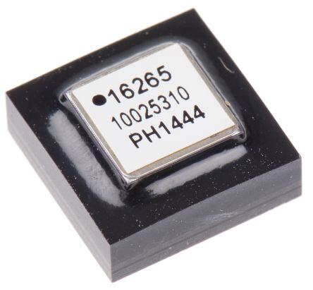
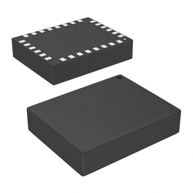
ICGOO电子元器件商城为您提供ADIS16265BCCZ由Analog设计生产,在icgoo商城现货销售,并且可以通过原厂、代理商等渠道进行代购。 ADIS16265BCCZ价格参考。AnalogADIS16265BCCZ封装/规格:运动传感器 - 陀螺仪, Gyroscope Z (Yaw) ±80, 160, 320 50Hz ~ 330Hz SPI 20-LGA (11x11)。您可以下载ADIS16265BCCZ参考资料、Datasheet数据手册功能说明书,资料中有ADIS16265BCCZ 详细功能的应用电路图电压和使用方法及教程。
ADIS16265BCCZ 是由 Analog Devices Inc.(ADI)生产的一款高性能运动传感器,属于陀螺仪类别。该型号是一款全集成的双轴陀螺仪模块,广泛应用于需要高精度角度测量和运动检测的场景。以下是其主要应用场景:

1. 工业自动化与机器人
   ADIS16265BCCZ 可用于工业机器人的姿态控制、位置校正和路径规划。它能够实时监测机器人的旋转角度和速度,确保精准的动作执行和稳定性。

2. 无人机与飞行器稳定系统
   在无人机和小型飞行器中,这款陀螺仪可以提供精确的角速度数据,用于飞行姿态调整、航向稳定以及防抖功能,从而提升飞行性能和拍摄质量。

3. 导航与定位系统
   作为惯性导航系统的一部分,ADIS16265BCCZ 能够在 GPS 信号弱或无信号的情况下,通过测量物体的旋转运动来辅助定位,适用于车辆、船舶或航空器的导航。

4. 医疗设备
   在康复设备、步态分析仪器或手术机器人中,该陀螺仪可用于监测患者的身体运动或机械臂的姿态变化,以实现精准控制和数据分析。

5. 振动监测与结构健康检测
   该器件可安装于桥梁、建筑或其他大型结构上,用于检测微小的振动或倾斜,帮助评估结构完整性并预防潜在的安全隐患。

6. 消费电子产品
   在高端相机、摄像机或虚拟现实(VR)/增强现实(AR)设备中,ADIS16265BCCZ 提供高精度的运动跟踪能力,支持图像稳定和交互式体验。

7. 军事与航空航天
   此类高精度陀螺仪常用于导弹制导、飞机姿态控制或卫星姿态调整等关键任务中,确保系统的可靠性和准确性。

ADIS16265BCCZ 的核心优势在于其卓越的稳定性和抗噪能力,能够在恶劣环境下保持高精度输出,因此适合对可靠性要求极高的应用场合。
| 参数 | 数值 |
| 产品目录 | |
| 描述 | IC SENSOR GYRO PROGR 10MV 20LGA螺旋仪 Programmable Digital Sensor |
| 产品分类 | 陀螺仪运动与定位传感器 |
| 品牌 | Analog Devices |
| 产品手册 | |
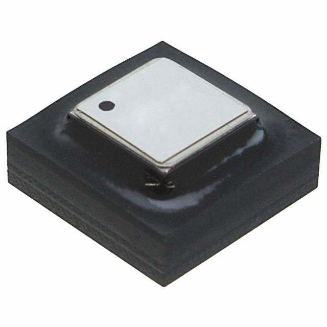
| 产品图片 |
|
| rohs | RoHS 合规性豁免无铅 / 符合限制有害物质指令(RoHS)规范要求 |
| 产品系列 | 螺旋仪,Analog Devices ADIS16265BCCZMEMS |
| 数据手册 | |
| 产品型号 | ADIS16265BCCZ |
| 产品种类 | 螺旋仪 |
| 传感轴 | Z |
| 供应商器件封装 | 20-LGA(11x11) |
| 典型带宽 | 50Hz |
| 加速 | 2000 g |
| 商标 | Analog Devices |
| 宽度 | 11.2 mm |
| 封装 | Tray |
| 封装/外壳 | 20-BLGA |
| 封装/箱体 | LGA-20 |
| 工作温度 | -40°C ~ 105°C |
| 工厂包装数量 | 176 |
| 带宽 | 335 Hz |
| 数字输出-位数 | 12 bit |
| 数字输出-总线接口 | SPI |
| 最大工作温度 | + 105 C |
| 最小工作温度 | - 40 C |
| 标准包装 | 1 |
| 灵敏度 | 0.07326 deg/s/LSB |
| 电压-电源 | 4.75 V ~ 5.25 V |
| 电流-电源 | 41mA |
| 电源电压-最大 | 5.25 V |
| 电源电压-最小 | 4.75 V |
| 电源电流 | 41 mA |
| 系列 | ADIS16265 |
| 范围 | +/- 80 deg/s, +/- 160 deg/s, +/- 320 deg/s |
| 范围°/s | ±80°/s, ±160°/s, ±320°/s |
| 输出类型 | Digital |
| 长度 | 11.2 mm |
| 高度 | 5.5 mm |


- 商务部:美国ITC正式对集成电路等产品启动337调查
- 曝三星4nm工艺存在良率问题 高通将骁龙8 Gen1或转产台积电
- 太阳诱电将投资9.5亿元在常州建新厂生产MLCC 预计2023年完工
- 英特尔发布欧洲新工厂建设计划 深化IDM 2.0 战略
- 台积电先进制程称霸业界 有大客户加持明年业绩稳了
- 达到5530亿美元!SIA预计今年全球半导体销售额将创下新高
- 英特尔拟将自动驾驶子公司Mobileye上市 估值或超500亿美元
- 三星加码芯片和SET,合并消费电子和移动部门,撤换高东真等 CEO
- 三星电子宣布重大人事变动 还合并消费电子和移动部门
- 海关总署:前11个月进口集成电路产品价值2.52万亿元 增长14.8%

PDF Datasheet 数据手册内容提取
Programmable Digital Gyroscope Sensor Data Sheet ADIS16260/ADIS16265 FEATURES GENERAL DESCRIPTION Yaw rate gyroscope with range scaling The ADIS16260 and the ADIS16265 are programmable digital ±80°/sec, ±160°/sec, and ±320°/sec settings gyroscopes that combine industry-leading MEMS and signal No external configuration required to start data collection processing technology in a single compact package. They provide Start-up time: 165 ms accuracy performance that would require full motion calibration Sleep mode recovery time: 2.5 ms with any other MEMS gyroscope in their class. When power is Factory-calibrated sensitivity and bias applied, the ADIS16260 and the ADIS16265 automatically start up ADIS16265 calibration temperature range: −40°C to +85°C and begin sampling sensor data, without requiring configuration ADIS16260 calibration temperature: +25°C commands from a system processor. An addressable register SPI-compatible serial interface structure and a common serial peripheral interface (SPI) provide Relative angle displacement output simple access to sensor data and configuration settings. Many Embedded temperature sensor digital processor platforms support the SPI with simple firmware- Programmable operation and control level instructions. Automatic and manual bias correction controls The ADIS16260 and the ADIS16265 provide several programmable Sensor bandwidth selection: 50 Hz/330 Hz features for in-system optimization. The sensor bandwidth switch Sample rate: 256 SPS/2048 SPS settings (50 Hz and 330 Hz), Bartlett window FIR filter length, and sample Bartlett window FIR filter length, number of taps rate settings provide users with controls that enable noise vs. Digital I/O: data ready, alarm indicator, general-purpose bandwidth optimization. The digital input/output lines offer Alarms for condition monitoring options for a data ready signal that helps the master processor Sleep mode for power management efficiently manage data coherency, an alarm indicator signal for DAC output voltage triggering master processor interrupts, and a general-purpose Single-command self-test function for setting and monitoring system-level digital controls/ Single-supply operation: 4.75 V to 5.25 V conditions. 3.3 V compatible digital lines 2000 g shock survivability The ADIS16260 and the ADIS16265 come in a LGA package Operating temperature range: −40°C to +105°C (11.2 mm × 11.2mm × 5.5 mm), which supports Pb-free solder reflow assembly, in accordance with JEDEC J-STD-020. They APPLICATIONS have an extended operating temperature range of −40°C to +105°C. Platform control and stabilization Navigation Medical instrumentation Robotics FUNCTIONAL BLOCK DIAGRAM DIO1DIO2 RST VCC SELF-TEST OINUPTUPTU/T ALARMS MANPAOGWEEMRENT GND MEMS RATE GYROSCOPE SENSOR FILT USER TEMPERATURE CONTROLLER CONTROL SENSOR REGISTERS CS POWER SCLK AUX SUPPLY CLOCK FILTER PSOPRIT ADC OUTPUT DIN VREF DATA REGISTERS DOUT DAAUCX ADIS16260/ADIS16265 CALIBRATION 08246-001 Figure 1. Rev. F Document Feedback Information furnished by Analog Devices is believed to be accurate and reliable. However, no responsibility is assumed by Analog Devices for its use, nor for any infringements of patents or other One Technology Way, P.O. Box 9106, Norwood, MA 02062-9106, U.S.A. rights of third parties that may result from its use. Specifications subject to change without notice. No license is granted by implication or otherwise under any patent or patent rights of Analog Devices. Tel: 781.329.4700 ©2009–2018 Analog Devices, Inc. All rights reserved. Trademarks and registered trademarks are the property of their respective owners. Technical Support www.analog.com
ADIS16260/ADIS16265 Data Sheet TABLE OF CONTENTS Features .............................................................................................. 1 SPI Write Commands ................................................................ 11 Applications ....................................................................................... 1 SPI Read Commands ................................................................. 11 General Description ......................................................................... 1 Memory Map .............................................................................. 12 Functional Block Diagram .............................................................. 1 Processing Sensor Data ............................................................. 13 Revision History ............................................................................... 2 Operational Controls ................................................................. 13 Specifications ..................................................................................... 3 Input/Output Functions ............................................................ 15 Timing Specifications .................................................................. 5 Diagnostics .................................................................................. 16 Absolute Maximum Ratings ............................................................ 6 Product Identification ................................................................ 17 ESD Caution .................................................................................. 6 Applications Information .............................................................. 18 Pin Configuration and Function Descriptions ............................. 7 Assembly ...................................................................................... 18 Typical Performance Characteristics ............................................. 8 Bias Optimization ....................................................................... 18 Theory of Operation ........................................................................ 9 Interface Printed Circuit Board ................................................ 18 Sensing Element ........................................................................... 9 Outline Dimensions ....................................................................... 20 Data Sampling and Processing ................................................... 9 Ordering Guide .......................................................................... 20 User Interface ................................................................................ 9 Basic Operation .......................................................................... 10 REVISION HISTORY 9/2018—Rev. E to Rev. F 12/2010—Rev. A to Rev. B Changes to General Description Section ...................................... 1 Changes to Equation in Internal Sample Rate Section .............. 13 Changes to Assembly Section, Interface Printed Circuit Board Changes to Figure 15 ...................................................................... 14 Section, and Figure 19 .................................................................... 18 Changes to Bias Optimization Section ........................................ 18 Changes to Ordering Guide .......................................................... 20 10/2009—Rev. 0 to Rev. A 1/2014—Rev. D to Rev. E Added ADIS16260 .............................................................. Universal Change to Table 3 ............................................................................. 6 Changes to Features List and General Description Section ........ 1 Change to Bias Optimization Section .......................................... 18 Changes to Table 1 ............................................................................. 4 Change to Absolute Maximum Ratings Table Section ................. 6 10/2011—Rev. C to Rev. D Changes to Interface Printed Circuit Board Section ................. 18 Change to Step 9, Bias Optimization Section ............................. 18 Changes to Ordering Guide .......................................................... 20 5/2011—Rev. B to Rev. C 9/2009—Revision 0: Initial Version Changes to Bias Optimization Section ........................................ 18 Rev. F | Page 2 of 20
Data Sheet ADIS16260/ADIS16265 SPECIFICATIONS T = −40°C to +105°C, V = 5.0 V, angular rate = 0°/sec, ±1 g, ±320°/sec range setting, unless otherwise noted. A CC Table 1. Parameter Test Conditions/Comments Min Typ Max Unit SENSITIVITY1 Clockwise rotation is positive output 25°C, dynamic range = ±320°/sec2 0.07326 °/sec/LSB 25°C, dynamic range = ±160°/sec 0.03663 °/sec/LSB 25°C, dynamic range = ±80°/sec 0.01832 °/sec/LSB Initial Tolerance 25°C, dynamic range = ±320°/sec ±0.2 ±1 % Temperature Coefficient ADIS16260 125 ppm/°C ADIS16265 25 ppm/°C Nonlinearity Best fit straight line 0.1 % of FS BIAS In-Run Bias Stability 25°C, 1σ 0.007 °/sec Turn-On-to-Turn-On Bias Stability 25°C, 1σ 0.025 °/sec Angular Random Walk 25°C, 1σ 2 °/√hour Temperature Coefficient ADIS16260 0.03 °/sec/°C ADIS16265 0.005 °/sec/°C Linear Acceleration Effect Any axis 0.2 °/sec/g Voltage Sensitivity V = 4.75 V to 5.25 V 0.5 °/sec/V CC NOISE PERFORMANCE Output Noise 25°C, ±320°/sec range, no filtering, 50 Hz, 256 SPS 0.4 °/sec rms 25°C, ±320°/sec range, no filtering, 330 Hz, 2048 SPS 0.9 °/sec rms 25°C, ±160°/sec range, 4-tap filter setting, 50 Hz 0.2 °/sec rms 25°C, ±80°/sec range, 16-tap filter setting, 50 Hz 0.1 °/sec rms Rate Noise Density 25°C, f = 25 Hz, ±320°/sec range, no filtering 0.044 °/sec/√Hz rms FREQUENCY RESPONSE 3 dB Bandwidth SENS_AVG[7] = 0 50 Hz SENS_AVG[7] = 1 330 Hz Sensor Resonant Frequency 14 kHz SELF-TEST STATE Change for Positive Stimulus 320°/sec dynamic range setting +575 +1100 +1500 LSB Change for Negative Stimulus 320°/sec dynamic range setting −575 −1100 −1500 LSB Internal Self-Test Cycle Time 25 ms ADC INPUT Resolution 12 Bits Integral Nonlinearity ±2 LSB Differential Nonlinearity ±1 LSB Offset Error ±4 LSB Gain Error ±2 LSB Input Range 0 2.5 V Input Capacitance During acquisition 20 pF ON-CHIP VOLTAGE REFERENCE 2.5 V Accuracy 25°C −10 +10 mV Temperature Coefficient ±40 ppm/°C Output Impedance 70 Ω Rev. F | Page 3 of 20
ADIS16260/ADIS16265 Data Sheet Parameter Test Conditions/Comments Min Typ Max Unit DAC OUTPUT 5 kΩ/100 pF to GND Resolution 12 Bits Relative Accuracy For Code 101 to Code 4095 4 LSB Differential Nonlinearity 1 LSB Offset Error ±5 mV Gain Error ±0.5 % Output Range 0 2.5 V Output Impedance 2 Ω Output Settling Time 10 µs LOGIC INPUTS Internal 3.3 V interface Input High Voltage, V 2.0 V INH Input Low Voltage, V 0.8 V INL Logic 1 Input Current, I V = 3.3 V ±0.2 ±10 µA INH IH Logic 0 Input Current, I V = 0 V INL IL All Except RST −40 −60 µA RST The RST pin has an internal pull-up. −1 mA Input Capacitance, C 10 pF IN DIGITAL OUTPUTS Internal 3.3 V interface Output High Voltage, V I = 1.6 mA 2.4 V OH SOURCE Output Low Voltage, V I = 1.6 mA 0.4 V OL SINK SLEEP TIMER Timeout Period3 0.5 128 sec START-UP TIME Initial Start-Up Time 165 ms Sleep Mode Recovery 2.5 ms Flash Update Time 50 ms Flash Test Process Time Normal mode, SMPL_PRD[7:0] ≤ 0x07 18 ms Low power mode, SMPL_PRD[7:0] ≥ 0x08 70 ms FLASH MEMORY Endurance4 20,000 Cycles Data Retention5 T = 55°C 10 Years J CONVERSION RATE Minimum Conversion Time SMPL_PRD[7:0] = 0x00 0.488 ms Maximum Conversion Time SMPL_PRD[7:0] = 0xFF 7.75 sec Maximum Throughput Rate SMPL_PRD[7:0] = 0x00 2048 SPS Minimum Throughput Rate SMPL_PRD[7:0] = 0xFF 0.129 SPS POWER SUPPLY Operating Voltage Range, V 4.75 5.0 5.25 V CC Power Supply Current Low power mode, SMPL_PRD[7:0] ≥ 0x08 17 mA Normal mode, SMPL_PRD[7:0] ≤ 0x07 41 mA Sleep mode 350 µA 1 ADIS16260/ADIS16265 characterization data represents ±4σ to fall within the ±1% limit. 2 The maximum guaranteed measurement range is ±320°/sec. The sensor outputs will measure beyond this range, but performance is not assured. 3 Guaranteed by design. 4 Endurance is qualified as per JEDEC Standard 22, Method A117, and measured at −40°C, +25°C, +85°C, and +125°C. 5 Retention lifetime equivalent at a junction temperature (TJ) of 55°C, as per JEDEC Standard 22, Method A117. Retention lifetime decreases with junction temperature. Rev. F | Page 4 of 20
Data Sheet ADIS16260/ADIS16265 TIMING SPECIFICATIONS T = −40°C to +85°C, V = 5.0 V, unless otherwise noted. A CC Table 2. Normal Mode Low Power Mode (SMPL_PRD[7:0] ≤ 0x07, f ≥ 64 Hz) (SMPL_PRD[7:0] ≥ 0x08, f ≤ 56.9 Hz) S S Parameter Description Min1 Typ Max1 Min1 Typ Max1 Unit f Serial clock 0.01 2.5 0.01 1.0 MHz SCLK t Data rate period 32 42 μs DATARATE t Stall period between data 9 12 μs STALL t Chip select to clock edge 48.8 48.8 ns CS t Data output valid after SCLK falling 100 100 ns DAV edge2 t Data input setup time before SCLK 24.4 24.4 ns DSU rising edge t Data input hold time after SCLK 48.8 48.8 ns DHD rising edge t Data output fall time 5 12.5 5 12.5 ns DF t Data output rise time 5 12.5 5 12.5 ns DR t CS high after SCLK edge3 5 5 ns SFS 1 Guaranteed by design; not production tested. 2 The MSB presents an exception to this parameter. The MSB clocks out on the falling edge of CS. The rest of the DOUT bits are clocked after the falling edge of SCLK and are governed by this specification. 3 This parameter may need to be expanded to allow for proper capture of the LSB. After CS goes high, the DOUT line goes into a high impedance state. Timing Diagrams t DATARATE CS SCLK tSTALL 08246-002 Figure 2. SPI Chip Select Timing CS t t CS SFS 1 2 3 4 5 6 15 16 SCLK t DAV DOUT * MSB DB14 DB13 DB12 DB11 DB10 DB2 DB1 LSB t t DSU DHD DIN R/W A5 A4 A3 A2 D2 D1 LSB *NOT DEFINED 08246-003 Figure 3. SPI Timing (Using SPI Settings Typically Identified as CPOL = 1, CPHA = 1) Rev. F | Page 5 of 20
ADIS16260/ADIS16265 Data Sheet ABSOLUTE MAXIMUM RATINGS Stresses at or above those listed under Absolute Maximum Table 3. Ratings may cause permanent damage to the product. This is a Parameter Rating stress rating only; functional operation of the product at these Acceleration or any other conditions above those indicated in the operational Any Axis, Unpowered, 0.5 ms 2000 g section of this specification is not implied. Operation beyond Any Axis, Powered, 0.5 ms 2000 g the maximum operating conditions for extended periods may VCC to GND −0.3 V to +6.0 V affect product reliability. Digital Input/Output Voltage to GND −0.3 V to +5.3 V Analog Inputs to GND −0.3 V to +3.5 V Operating Temperature Range1 −40°C to +125°C ESD CAUTION Storage Temperature Range1 −65°C to +150°C 1 Extended exposure to temperatures outside the temperature range of −40°C to +85°C can adversely affect the accuracy of the factory calibration. For best accuracy, store the part within the temperature range of −40°C to +85°C. Rev. F | Page 6 of 20
Data Sheet ADIS16260/ADIS16265 PIN CONFIGURATION AND FUNCTION DESCRIPTIONS VREF GND GND VCC VCC 20 19 18 17 16 SCLK 1 ADIS16260/ 15 FILT ADIS16265 DOUT 2 TOP VIEW 14 RATE (Not to Scale) DIN 3 13 AUX ADC POSITIVE OUTPUT CS 4 ROTATIONAL 12 ADUAXC DIRECTION DIO1 5 11 DNC 6 7 8 9 10 DIO2 RST DNC DNC DNC NOTES 1. DNC = DO NOT CONNECT. 2.THE PINS CANNOT BE SEEN FROM THE TOP. TIPSHC OIBSF PLFAOETROTEKED-RT FNHOSO.RU GRHEF VEIERWEN OCFE TINH EDIERV LEOLCOAPTINIOGN 08246-005 Figure 4. Pin Configuration AXIS OF ROTATION PIN 1 PIN 10 PIN 5 PIN 6 NOTES 1TT.HH AAER TGR PYORRWOO D_INOUDCUIETCS AR TAEE GPSIO STSTHEIETRI VD.EIR REECSTPIOONN OSEF IRNOTATION 08246-022 Figure 5. Axial Orientation Table 4. Pin Function Descriptions Pin No. Mnemonic Type1 Description 1 SCLK I SPI Serial Clock. 2 DOUT O SPI Data Output. Clocks output on SCLK falling edge. 3 DIN I SPI Data Input. Clocks input on SCLK rising edge. 4 CS I SPI Chip Select. Active low. 5, 6 DIO1, DIO2 I/O Configurable Digital Input/Output. 7 RST I Reset. Active low. 8, 9, 10, 11 DNC Do Not Connect. 12 AUX DAC O Auxiliary DAC Output. 13 AUX ADC I Auxiliary ADC Input. 14 RATE O Rate Output. For bandwidth reduction only; output is not specified. 15 FILT I Filter Terminal. 16, 17 VCC S 5.0 V Power Supply. 18, 19 GND S Ground. 20 VREF O Precision Reference Output. 1 I = input, I/O = input/output, O = output, S = supply. Rev. F | Page 7 of 20
ADIS16260/ADIS16265 Data Sheet TYPICAL PERFORMANCE CHARACTERISTICS 1 c) e s (°/ E 0.1 C N A RI A V N LA MEAN AL 0.01 +1σ T O O R –1σ 0.001 0.1 1 Tau (S1e0conds) 100 1k 08246-020 Figure 6. Gyroscope Allan Variance Rev. F | Page 8 of 20
Data Sheet ADIS16260/ADIS16265 THEORY OF OPERATION The ADIS16260 and the ADIS16265 integrate a MEMS gyroscope USER INTERFACE with data sampling, signal processing, and calibration functions, SPI Interface along with a simple user interface. This sensing system collects Data collection and configuration commands both use the SPI, data autonomously and makes it available to any processor system which consists of four wires. The chip select (CS) signal activates that supports a 4-wire serial peripheral interface (SPI). the SPI interface, and the serial clock (SCLK) signal synchronizes SENSING ELEMENT the serial data lines. The serial input data clocks into DIN on The sensing element operates on the principle of a resonator the SCLK rising edge, and the serial output data clocks out of gyro. Two polysilicon sensing structures each contain a dither DOUT on the SCLK falling edge. Many digital processor plat- frame that is electrostatically driven to resonance, producing forms support this interface with dedicated serial ports and the necessary velocity element to produce a Coriolis force during simple instruction sets. angular rate. At two of the outer extremes of each frame, User Registers orthogonal to the dither motion, movable fingers are placed The user registers provide addressing for all input/output between fixed pickoff fingers to form a capacitive pickoff operations on the SPI interface. Each 16-bit register has its structure that senses Coriolis motion. The resulting signal is fed own unique bit assignment and has two 7-bit addresses: one into a series of gain and demodulation stages that produce the for its upper byte and one for its lower byte. Table 7 provides a electrical rate signal output. The differential structure minimizes memory map of the user registers, along with the function of the response to linear acceleration (gravity, vibration, and so each register. on) and to EMI. The control registers use a dual memory structure. The SRAM DATA SAMPLING AND PROCESSING controls operation while the part is on and facilitates all user The ADIS16260 and the ADIS16265 run autonomously, based configuration inputs. The flash memory provides nonvolatile on the configuration in the user control registers. The analog storage for control registers that have flash backup (see Table 7). gyroscope signal feeds into an analog-to-digital converter Storing configuration data in the flash memory requires a separate (ADC) stage, which passes digitized data into the controller for command (GLOB_CMD[3] = 1, DIN = 0xBE08). When the data processing and register loading. Data processing in the device powers on or resets, the flash memory contents are embedded controller includes correction formulas, filtering, loaded into the SRAM, and the device then starts producing and checking for preset alarm conditions. The correction formulas data according to the configuration in the control registers. are unique for each individual ADIS16260/ADIS16265 and come from the factory characterization of each device over a MANUAL temperature range of −40°C to +85°C. FLASH BACKUP NONVOLATILE VOLATILE MEMS FLASH MEMORY SRAM SENSOR OUTPUT REGISTERS S (NO SPIACCESS) SPIACCESS L A SETNEMSOPR SPI PORT ADC CONTROLLER CONTROL SPI PORT SPI SIGN OSRTA RRETSUEPT 08246-008 REGISTERS Figure 8. SRAM and Flash Memory Diagram AIN SIGNALS CLOCK 08246-007 Figure 7. Simplified Sensor Signal Processing Diagram Rev. F | Page 9 of 20
ADIS16260/ADIS16265 Data Sheet BASIC OPERATION The ADIS16260 and the ADIS16265 SPI interface supports full- The ADIS16260 and the ADIS16265 require only power, ground, duplex serial communication (simultaneous transmit and and the four SPI signals to produce data and make it available receive) and uses the bit sequence shown in Figure 11. Processor to an embedded processor. Figure 9 provides a schematic for platforms typically support SPI communication with general- connecting the ADIS16260 and the ADIS16265 to a SPI- purpose serial ports that require some configuration in their compatible processor and includes one of the configurable control registers. Table 6 provides a list of the most common digital I/O lines. The MSC_CTRL[2:0] bits are used to configure settings that require attention to initialize the serial port of a this line as a data ready indicator (see the Data Ready I/O processor for communication with the ADIS16260 and the Indicator section). ADIS16265. INPUT/OUTPUT LINESARE COMPATIBLE Table 6. Generic Master Processor SPI Settings WITH 3.3V OR 5V LOGIC LEVELS 5V Processor Setting Description VDD Master The ADIS16260 and the ADIS16265 16 17 operate as slaves VCC VCC SS 4 CS SCLK Rate ≤ 2.5 MHz Bit rate setting (SMPL_PRD[7:0] ≤ 0x07) SCLK 1 SCLK SPI Mode 3 Clock polarity, phase (CPOL = 1, CPHA = 1) SYSTEM ADIS16260/ PROCESSOR MOSI 3 DIN ADIS16265 MSB First Mode Bit sequence SPI MASTER SPI SLAVE 16-Bit Mode Shift register/data length MISO 2 DOUT User registers govern all data collection and configuration. IRQ 5 DIO1 GND GND Table 7 provides a memory map that includes all user registers, 18 19 08246-009 agleonnegr iwc ibtiht aresfseigrennmceesn ttso itnh eF ibgiut raes s1i0g.n ment tables that follow the Figure 9. Electrical Connection Diagram TPianb Nlea 5m. eG eneric MasteFru Pnrcotcioenss or Pin Names and Functions 15 14 13UPP1E2R B1Y1TE10 9 8 7 6 5LOW4ER B3YTE2 1 0 08246-010 SS Slave select Figure 10. Generic Register Bit Definitions IRQ Interrupt request input MOSI Master output, slave input MISO Master input, slave output SCLK Serial clock CS SCLK DIN R/W A6 A5 A4 A3 A2 A1 A0 D7 D6 D5 D4 D3 D2 D1 D0 R/W A6 A5 DOUT DB15 DB14DB13DB12DB11 DB10 DB9 DB8 DB7 DB6 DB5 DB4 DB3 DB2 DB1 DB0 DB15 DB14 DB13 N1.O DTOEUST BITS ARE BASED ON THE PREVIOUS 16-BIT SEQUENCE (R/W = 0). 08246-013 Figure 11. SPI Communication Bit Sequence Rev. F | Page 10 of 20
Data Sheet ADIS16260/ADIS16265 SPI WRITE COMMANDS SPI READ COMMANDS Master processors write to the control registers, one byte Reading data through the SPI requires two consecutive 16-bit at a time, using the bit sequence shown in Figure 11. Some sequences, separated by an appropriate stall time (see Figure 2). configurations require writing both bytes to a register, which The first sequence transmits the read command and address on takes two separate 16-bit sequences, whereas others require DIN, and the second receives the resulting data from DOUT. The only one byte. The programmable registers in Table 7 provide 7-bit register address can represent either the upper or lower byte controls for optimizing sensor operation and for starting various address for the target register. For example, when reading the automated functions. For example, to start an automatic bias GYRO_OUT register, the address can be either 0x04 or 0x05. null sequence, set GLOB_CMD[0] = 1 by writing 0xBE01 to the Figure 13 provides a full-duplex mode example of reading the SPI transmit register of the master processor, which feeds the GYRO_OUT register. In addition, the second SPI segment sets DIN line. The process starts immediately after the last bit clocks the device up to read TEMP_OUT on the following SPI segment into DIN (16th SCLK rising edge). (not shown in Figure 13). CS SCLK DIN 08246-011 Figure 12. SPI Sequence for Autonull (DIN = 0xBE01) CS SPI SEGMENT 1 SPI SEGMENT 2 SCLK DIN DIN = 0DxO04U0T0 DPURROIDNUGC TEHSE G NYERXOT_ SOPUI TS CEGOMNTEENNTTS ON DOUT DOUT = 0x822B = 21.9047°/sec, NEW DATA, NOALARM 08246-012 Figure 13. Example SPI Read Sequence (±320°/sec Range Setting) Rev. F | Page 11 of 20
ADIS16260/ADIS16265 Data Sheet MEMORY MAP All unused memory locations are reserved for future use. Table 7. User Register Memory Map Flash Bit Name Access Backup Address1 Default Register Description Assignments FLASH_CNT Read only Yes 0x00 N/A Flash memory write count SUPPLY_OUT Read only No 0x02 N/A Output, power supply measurement See Table 9 GYRO_OUT Read only No 0x04 N/A Output, rate of rotation measurement See Table 10 0x06 to 0x09 N/A Reserved AUX_ADC Read only No 0x0A N/A Output, analog input channel measurement See Table 13 TEMP_OUT Read only No 0x0C N/A Output, internal temperature measurement See Table 12 ANGL_OUT Read/write No 0x0E N/A Output, angle displacement See Table 11 0x10 to 0x13 N/A Reserved GYRO_OFF Read/write Yes 0x14 0x0000 Calibration, offset/bias adjustment See Table 16 GYRO_SCALE Read/write Yes 0x16 0x0800 Calibration, scale adjustment See Table 17 0x18 to 0x1F N/A Reserved ALM_MAG1 Read/write Yes 0x20 0x0000 Alarm 1 magnitude/polarity setting See Table 26 ALM_MAG2 Read/write Yes 0x22 0x0000 Alarm 2 magnitude/polarity setting See Table 26 ALM_SMPL1 Read/write Yes 0x24 0x0000 Alarm 1 dynamic rate of change setting See Table 27 ALM_SMPL2 Read/write Yes 0x26 0x0000 Alarm 2 dynamic rate of change setting See Table 27 ALM_CTRL Read/write Yes 0x28 0x0000 Alarm control register See Table 28 0x2A to N/A Reserved 0x2F AUX_DAC Read/write No 0x30 0x0000 Control, DAC output voltage setting See Table 22 GPIO_CTRL Read/write No 0x32 N/A Control, digital I/O line See Table 20 MSC_CTRL Read/write Yes 0x34 0x0000 Control, data ready, self-test settings See Table 21 SMPL_PRD Read/write Yes 0x36 0x0001 Control, internal sample rate See Table 14 SENS_AVG Read/write Yes 0x38 0x0402 Control, dynamic range, filtering See Table 15 SLP_CNT Read/write Yes 0x3A 0x0000 Control, sleep mode initiation See Table 19 DIAG_STAT Read only No 0x3C N/A Diagnostic, error flags See Table 25 GLOB_CMD Write only No 0x3E N/A Control, global commands See Table 18 0x40 to 0x51 N/A Reserved LOT_ID1 Read only Yes 0x52 N/A Lot Identification Code 1 See Table 31 LOT_ID2 Read only Yes 0x54 N/A Lot Identification Code 2 See Table 31 PROD_ID Read only Yes 0x56 0x3F89/0x3F84 Product identifier; convert to decimal = See Table 31 16,265/16,260 SERIAL_NUM Read only Yes 0x58 N/A Serial number See Table 31 1 Each register contains two bytes. The address of the lower byte is displayed. The address of the upper byte is equal to the address of the lower byte plus 1. Rev. F | Page 12 of 20
Data Sheet ADIS16260/ADIS16265 PROCESSING SENSOR DATA Table 11. ANGL_OUT Data Format Examples Table 8 provides a summary of the output data registers, which Angle1 Decimal Hex Binary Output use the bit pattern shown in Figure 14. The ND bit is equal to 1 359.9630° 9827 LSB 0x2663 10 0110 0110 0011 when the register contains unread data. The EA bit is high when 359.9264° 9826 LSB 0x2662 10 0110 0110 0010 any error/alarm flag in the DIAG_STAT register is equal to 1. 0.36630° 10 LSB 0x000A 00 0000 0000 1010 0.03663° 1 LSB 0x0001 00 0000 0000 0001 MSB FOR 14-BIT OUTPUT 0° 0 LSB 0x0000 00 0000 0000 0000 ND EA MSB FOR 12-BIT OUTPUT 08246-021 1 359.963° + 1 LSB is equal to 0x0000. Figure 14. Output Register Bit Assignments Table 12. TEMP_OUT Data Format Examples Table 8. Output Data Register Formats Temperature Decimal Hex Binary Output Register Bits Scale Reference +105°C +551 LSB 0x227 0010 0010 0111 SUPPLY_OUT 12 1.8315 mV See Table 9 +25.1453°C +1 LSB 0x001 0000 0000 0001 GYRO_OUT1 14 0.07326°/sec See Table 10 +25°C 0 LSB 0x000 0000 0000 0000 ANGL_OUT 14 0.03663° See Table 11 +24.8547°C −1 LSB 0xFFF 1111 1111 1111 TEMP_OUT2 12 0.1453°C See Table 12 −40°C −447 LSB 0xE41 1110 0100 0001 AUX_ADC 12 610.5 μV See Table 13 1 Assumes that the scaling is set to ±320°/sec. This factor scales with the range. Table 13. AUX_ADC Data Format Examples 2 0x0000 = 25°C (±5°C). Input (mV) Decimal Hex Binary Output 2500 4095 LSB 0xFFF 1111 1111 1111 Table 9. SUPPLY_OUT Data Format Examples 1200 1966 LSB 0x7AE 0111 1010 1110 Supply Voltage (V) Decimal Hex Binary Output 0.6105 1 LSB 0x001 0000 0000 0001 5.25 2867 LSB 0xB33 1011 0011 0011 0 0 LSB 0x000 0000 0000 0000 5.0 + 0.00183 2731 LSB 0xAAB 1010 1010 1011 5.0 2730 LSB 0xAAA 1010 1010 1010 OPERATIONAL CONTROLS 5.0 − 0.00183 2729 LSB 0xAA9 1010 1010 1001 4.75 2594 LSB 0xA22 1010 0010 0010 Internal Sample Rate The SMPL_PRD register controls the internal sample rate using the bit assignments in Table 14. When SMPL_PRD[7:0] = 0x00, the Table 10. GYRO_OUT Data Format Examples internal sample rate is 2048 SPS. When SMPL_PRD[7:0] ≥ 0x01, Rotation Rate use the bit definitions in Table 14 and the following equation to (°/sec)1 Decimal Hex Binary Output calculate the sample rate. +320 +4368 LSB 0x1110 01 0001 0001 0000 +0.07326 +1 LSB 0x0001 00 0000 0000 0001 1 1 f 0 0 LSB 0x0000 00 0000 0000 0000 S t t (N 1) S B S −0.07326 −1 LSB 0x3FFF 11 1111 1111 1111 −320 −4368 LSB 0x2EF0 10 1110 1111 0000 Table 14. SMPL_PRD Bit Descriptions Bits Description (Default = 0x0001) 1 For the ±320°/sec setting, rate values scale with the range setting. [15:8] Not used 7 Time base (t): 0 = 1.953 ms, 1 = 60.54 ms B [6:0] Increment setting (N) S Rev. F | Page 13 of 20
ADIS16260/ADIS16265 Data Sheet Sensor Bandwidth Dynamic Range The gyroscope signal chain has several filter stages that shape The SENS_AVG[10:8] bits provide three dynamic range settings its frequency response. Figure 15 provides a block diagram of for this gyroscope. The lower dynamic range settings (±80°/sec each filter stage and Table 15 lists the SENS_AVG register and ±160°/sec) limit the minimum filter tap sizes to maintain controls for bandwidth. resolution. For example, set SENS_AVG[10:8] = 010 (DIN = 0xB902) for a measurement range of ±160°/sec. Because this Ce setting can influence the filter settings, program SENS_AVG[10:8] RATE FILT and then SENS_AVG[2:0] if more filtering is required. FROM Calibration GYRO N N SENSOR fC 740Hz The GYRO_OFF and GYRO_SCALE registers provide user fRCC T = == 9 C02kIN Ω T ×+ 1RC e× CT Nm == 2SmENS_AVG[2:0] 08246-014 cfaocnttorro. ls for making in-system adjustments to offset and scale Figure 15. Signal Processing Diagram FROM INTERNAL TO OUTPUT PROCESSING REGISTERS TBiatbs le 15. SDENesSc_rAipVtiGon B (iDt eDfaeuscltr i=p t0ixo0n4s0 2) GYRO_OFF GYRO_SCALE 08246-016 [15:11] Not used. Figure 17. User Calibration Registers [10:8] Measurement range (sensitivity) selection. Table 16. GYRO_OFF Bit Descriptions 100 = ±320°/sec (default condition). Bits Description (Default = 0x0000) 010 = ±160°/sec, filter taps ≥ 4 (Bits[2:0] ≥ 0x02). [15:12] Not used. 001 = ±80°/sec, filter taps ≥ 16 (Bits[2:0] ≥ 0x04). [11:0] Offset adjustment factor, twos complement format, 7 Primary pole setting (k). 0.018315°/sec per LSB. 1: C = 0.0047 μF (bandwidth = 330 Hz). INT Examples follow: 0: C = 0.0377 μF (bandwidth = 50 Hz). INT 0x000: Add 0°/sec to gyroscope data. [6:3] Not used. 0x001: Add 0.018315°/sec to gyroscope data. [2:0] Number of taps in each stage; value of m in N = 2m. 0x0AA: Add 3.11355°/sec to gyroscope data. 0xF0F: Subtract 4.41392°/sec from gyroscope data. Digital Filtering 0xFFF: Subtract 0.018315°/sec from gyroscope data. A programmable low-pass filter provides additional opportunity for noise reduction on the inertial sensor outputs. This filter Table 17. GYRO_SCALE Bit Descriptions contains two cascaded averaging filters that provide a Bartlett Bits Description (Default = 0x0800) window, FIR filter response (see Figure 16). For example, set [15:12] Not used. SENS_AVG[2:0] = 100 (DIN = 0xB804) to set each stage to 16 [11:0] Scale adjustment factor, offset binary format, taps. When used with the default sample rate of 256 SPS, this 0.00048828/LSB. reduces the bandwidth of the digital filter to approximately 5.2 Hz. Examples follow: 0 0x000: Multiply output by 0. 0x7F0: Multiply gyroscope data by 0.99218. –20 0x800: Multiply output by 1. –40 0x8A0: Multiply output by 1.077812. B) 0xFFF: Multiply output by 1.9995. d E ( –60 D U T NI –80 G A M –100 N = 2 –120 N = 4 N = 16 N = 64 –140 0.001 0.01FREQUENCY (f/fS)0.1 108246-015 Figure 16. Digital Filter Frequency, Bartlett Window FIR Filter (Phase = N Samples) Rev. F | Page 14 of 20
Data Sheet ADIS16260/ADIS16265 Global Commands Data Ready I/O Indicator The GLOB_CMD register provides trigger bits for several The MSC_CTRL[2:0] bits configure one of the digital I/O lines functions. Setting the assigned bit to 1 starts each operation, as a data ready signal for driving an interrupt. For example, set which returns the bit to 0 after completion. For example, set MSC_CTRL[2:0] = 100 (DIN = 0xB404) to configure DIO1 as GLOB_CMD[7] = 1 (DIN = 0xBE80) to execute a software a negative-pulse data ready signal. The pulse width is between reset, which stops the sensor operation and runs the device 100 µs and 200 µs over all conditions. through its start-up sequence. This sequence includes loading Table 21. MSC_CTRL Bit Descriptions the control registers with the contents of their respective flash Bits Description (Default = 0x0000) memory locations prior to producing new data. [15:12] Not used. Table 18. GLOB_CMD Bit Descriptions 11 Memory test (cleared upon completion). Bits Description 1 = enabled, 0 = disabled. [15:8] Not used. 10 Internal self-test enable (cleared upon completion). 7 Software reset command. 1 = enabled, 0 = disabled. [6:4] Not used. 9 Manual self-test, negative stimulus. 3 Flash update command. 1 = enabled, 0 = disabled. 2 Auxiliary DAC data latch. 8 Manual self-test, positive stimulus. 1 Factory calibration restore command. 1 = enabled, 0 = disabled. 0 Autonull command. [7:3] Not used. 2 Data ready enable. Power Management 1 = enabled, 0 = disabled. 1 Data ready polarity. Setting SMPL_PRD[7:0] ≥ 0x08 also sets the sensor to low 1 = active high, 0 = active low. power mode. For systems that require lower power dissipation, 0 Data ready line select. in-system characterization helps users to quantify the associated 1 = DIO2, 0 = DIO1. performance trade-offs. In addition to sensor performance, low power mode affects SPI data rates (see Table 2). Use SLP_CNT[7:0] Auxiliary DAC to put the device into sleep mode for a specified period. For example, SLP_CNT[7:0] = 0x64 (DIN = 0xBA64) puts the The 12-bit AUX_DAC line can drive its output to within 5 mV ADIS16260 and ADIS16265 to sleep for 50 seconds. of the ground reference when it is not sinking current. As the output approaches 0 V, the linearity begins to degrade (~100 LSB Table 19. SLP_CNT Bit Descriptions starting point). As the sink current increases, the nonlinear Bits Description (Default = 0x0000) range increases. The DAC latch command moves the values of [15:8] Not used. the AUX_DAC register into the DAC input register, enabling [7:0] Programmable sleep time bits, 0.5 sec/LSB. both bytes to take effect at the same time. INPUT/OUTPUT FUNCTIONS Table 22. AUX_DAC Bit Descriptions General-Purpose I/O Bits Description (Default = 0x0000) DIO1 and DIO2 are configurable, general-purpose I/O lines [15:12] Not used. that serve multiple purposes according to the following control [11:0] Data bits, scale factor = 0.6105 mV/code. register priority: MSC_CTRL, ALM_CTRL, and GPIO_CTRL. Offset binary format, 0 V = 0 codes. For example, set GPIO_CTRL = 0x0202 (DIN = 0xB302, and then 0xB202) to configure DIO1 as an input and DIO2 as an Table 23. Setting AUX_DAC = 2 V output set high. DIN Description Table 20. GPIO_CTRL Bit Descriptions 0xB0CC AUX_DAC[7:0] = 0xCC (204 LSB). Bits Description 0xB10C AUX_DAC[15:8] = 0x0C (3072 LSB). [15:10] Not used. 0xBE04 GLOB_CMD[2] = 1. Move values into the DAC input register, resulting in 9 General-Purpose I/O Line 2 (DIO2) data level. a 2 V output level. 8 General-Purpose I/O Line 1 (DIO1) data level. [7:2] Not used. 1 General-Purpose I/O Line 2 (DIO2) direction control. 1 = output, 0 = input. 0 General-Purpose I/O Line 1 (DIO1) direction control. 1 = output, 0 = input. Rev. F | Page 15 of 20
ADIS16260/ADIS16265 Data Sheet Status DIAGNOSTICS Self-Test The error flags provide indicator functions for common system level issues. All of the flags are cleared (set to 0) after The self-test function allows the user to verify the mechanical each DIAG_STAT register read cycle. If an error condition integrity of each MEMS sensor. It applies an electrostatic force to remains, the error flag returns to 1 during the next sample each sensor element, which results in mechanical displacement cycle. DIAG_STAT[1:0] does not require a read of this register that simulates a response to actual motion. Table 1 lists the to return to 0. If the power supply voltage goes back into range, expected response for each sensor, which provides pass/fail these two flags are cleared automatically. criteria. Set MSC_CTRL[10] = 1 (DIN = 0xB504) to run the internal Table 25. DIAG_STAT Bit Descriptions self-test routine, which exercises the inertial sensor, measures Bits Description the response, makes a pass/fail decision, reports the decision to [15:10] Not used. error flags in the DIAG_STAT register, and then restores normal 9 Alarm 2 status (1 = active, 0 = inactive). operation. MSC_CTRL[10] resets itself to 0 after completing the 8 Alarm 1 status (1 = active, 0 = inactive). routine. The MSC_CTRL[9:8] bits provide manual control of the 7 Not used. self-test function for investigation of potential failures. Table 24 6 Flash test, checksum flag (1 = fail, 0 = pass). outlines an example test flow for using this option to verify the 5 Self-test diagnostic error flag (1 = fail, 0 = pass). gyroscope function. 4 Sensor overrange (1 = fail, 0 = pass). 3 SPI communication failure (1 = fail, 0 = pass). Table 24. Manual Self-Test Example Sequence 2 Flash update failure (1 = fail, 0 = pass). DIN Description 1 Power supply > 5.25 V. 0xB601 SMPL_PRD[7:0] = 0x01, sample rate = 256 SPS. 1 = power supply > 5.25 V, 0 = power supply ≤ 5.25 V. 0xB904 SENS_AVG[15:8] = 0x04, gyroscope range = 0 Power supply < 4.75 V. ±320°/sec. 1 = power supply < 4.75 V, 0 = power supply ≥ 4.75 V. 0xB802 SENS_AVG[7:0] = 0x02, four-tap averaging filter. Delay = 50 ms. 0x0400 Read GYRO_OUT. Alarm Registers 0xB502 MSC_CTRL[9:8] = 10, gyroscope negative self-test. The alarm function provides monitoring for two independent Delay = 50 ms. conditions. The ALM_CTRL register provides control inputs 0x0400 Read GYRO_OUT. for data source, data filtering (prior to comparison), static Determine whether the bias in the gyroscope comparison, dynamic rate-of-change comparison, and output output changed according to the self-test indicator configurations. The ALM_MAGx registers establish response specified in Table 1. the trigger threshold and polarity configurations. Table 29 gives 0xB501 MSC_CTRL[9:8] = 01, gyroscope/accelerometer positive self-test. an example of how to configure a static alarm. The ALM_SMPLx Delay = 50 ms. registers provide the numbers of samples to use in the dynamic 0x0400 Read GYRO_OUT. rate-of-change configuration. The period equals the number in Determine whether the bias in the gyroscope the ALM_SMPLx register multiplied by the sample period time, output changed according to the self-test which is established by the SMPL_PRD register. See Table 30 for response specified in Table 1. an example of how to configure the sensor for this type of function. 0xB500 MSC_CTRL[15:8] = 0x00. Table 26. ALM_MAG1, ALM_MAG2 Bit Descriptions Bits Description (Default = 0x0000) Zero motion provides results that are more reliable. The settings 15 Comparison polarity (1 = greater than, 0 = less than). in Table 24 are flexible and allow for optimization around speed 14 Not used. and noise influence. For example, using fewer filtering taps [13:0] Data bits that match the format of the trigger source decreases delay times but increases the potential for noise selection. influence. Memory Test Table 27. ALM_SMPL1, ALM_SMPL2 Bit Descriptions Bits Description (Default = 0x0000) Setting MSC_CTRL[11] = 1 (DIN = 0xB508) performs a checksum [15:8] Not used. comparison between the flash memory and SRAM to help [7:0] Data bits: number of samples (both 0x00 and 0x01 = 1). verify memory integrity. The pass/fail result is loaded into the DIAG_STAT[6] register. Rev. F | Page 16 of 20
Data Sheet ADIS16260/ADIS16265 Table 28. ALM_CTRL Bit Descriptions Table 30. Alarm Configuration Example 2 Bits Description (Default = 0x0000) DIN Description 15 Rate-of-change enable for Alarm 2 (1 = rate of change, 0xA9AA, 0xA804 ALM_CTRL = 0xAA04. 0 = static level). Alarm 1 input = GYRO_OUT. [14:12] Alarm 2 source selection. Alarm 2 input = GYRO_OUT. 000 = disable. Rate-of-change comparison, unfiltered data. 001 = power supply output. DIO1 output indicator, negative polarity. 010 = gyroscope output. 0xB601 SMPL_PRD = 0x0001. 011 = not used. Sample rate = 256 SPS. 100 = not used. 0xA40A ALM_SMPL1[7:0] = 0x000A. 101 = auxiliary ADC input. Alarm 1 rate of change period = 3.906 ms. 110 = temperature output. 0xA60A ALM_SMPL2[7:0] = 0x000A. 111 = not used. Alarm 2 rate of change period = 3.906 ms. 11 Rate-of-change enable for Alarm 1 (1 = rate of change, 0xA181, 0xA000 ALM_MAG1 = 0x8100. 0 = static level). Alarm 1 is true if GYRO_OUT changes more [10:8] Alarm 1 source selection (same as for Alarm 2). than 18.755°/sec over a period of 3.906 ms. [7:5] Not used. 0xA30F, 0xA200 ALM_MAG2 = 0x0F00. 4 Comparison data filter setting (1 = filtered data, 0 = Alarm 2 is true if GYRO_OUT changes less unfiltered data). than 18.755°/sec over a period of 3.906 ms. 3 Not used. 2 Alarm output enable (1 = enabled, 0 = disabled). PRODUCT IDENTIFICATION Table 31 provides a summary of the registers that identify 1 Alarm output polarity (1 = active high, 0 = active low). the product: PROD_ID, which identifies the product type; 0 Alarm output line select (1 = DIO2, 0 = DIO1). LOT_ID1 and LOT_ID2, the 32-bit lot identification code; and SERIAL_NUM, which displays the 16-bit serial number. Table 29. Alarm Configuration Example 1 All four registers are two bytes in length. DIN Description 0xA922, 0xA817 ALM_CTRL = 0x2217. Table 31. Identification Registers Alarm 1 input = GYRO_OUT. Register Name Address Description Alarm 2 input = GYRO_OUT. LOT_ID1 0x52 Lot Identification Code 1 Static level comparison, filtered data. LOT_ID2 0x54 Lot Identification Code 2 DIO2 output indicator, positive polarity. PROD_ID 0x56 Product identification = 0x3F89 or 0xA181, 0xA000 ALM_MAG1 = 0x8100. 0x3F84 Alarm 1 is true if GYRO_OUT > +18.755°/sec. (0x3F89 = 16,265 decimal; 0x3F84 = 0xA33F, 0xA200 ALM_MAG2 = 0x3F00. 16,260 decimal) Alarm 2 is true if GYRO_OUT < −18.755°/sec. SERIAL_NUM 0x58 Serial number Rev. F | Page 17 of 20
ADIS16260/ADIS16265 Data Sheet APPLICATIONS INFORMATION ASSEMBLY 7. Multiply by −1. 8. Write to GYRO_OFF. When developing a process flow for installing ADIS16260/ 9. Update flash, set GLOB_CMD[3] = 1 (DIN = 0xBE08), and ADIS16265 devices on printed circuit boards (PCBs), see wait for >50 ms and resume operation. the JEDEC J-STD-020C standard document for the reflow temperature profile and processing information. The ADIS16260/ The Allan Variance curve in Figure 6 provides a trade-off ADIS16265 can use the Sn-Pb eutectic process and the Pb-free relationship between accuracy and averaging time. For example, eutectic process from this standard, with one exception, the an average time of 1 second produce an accuracy of ~0.035 °/sec peak temperature exposure is 240°C. For a more complete list (1 σ). of assembly process suggestions, see the ADIS162xx LGA INTERFACE PRINTED CIRCUIT BOARD Assembly Guidelines page on Engineer Zone. Figure 18 provides an example pattern for the location of the The ADIS16265/PCBZ includes one ADIS16265BCCZ IC on a ADIS16260/ADIS16265 on a printed circuit board. 1.2 inch × 1.3 inch PCB. The interface PCB simplifies the IC connection of these devices to an existing processor system. The 5.0865 four mounting holes accommodate either M2 (2 mm) or 2-56 8× 3.800 8× machine screws. These boards are made of IS410 material and 0.773 are 0.063 inches thick. The second-level assembly uses a 16× SAC305-compatible solder composition, which has a presolder reflow thickness of approximately 0.005 inches. The pad pattern on these PCBs matches that shown in Figure 20. J1 and J2 are dual-row, 2 mm (pitch) connectors that work with 10.173 7.600 2× 4× a number of ribbon cable systems, including 3M Part Number 152212-0100-GB (ribbon crimp connector) and 3M Part Number 3625/12 (ribbon cable). The schematic and connector pin 0.500 20× assignments for the ADIS16265/PCBZ are shown in Figure 19. 12.102×7 08246-006 12 71 RSCSTLK AUX ADC 13 12 11mm × 11mm STACKED LGA PACKAGE 4 12 3 CS AUX DAC 3 Figure 18. Recommended Pad Layout (Units in Millimeters) 2 20 4 DOUT VREF 4 BIAS OPTIMIZATION 5 5 3 ADIS16265 6 DIN 6 Use the following steps to fine-tune the bias to an accuracy that 18 7 GND 7 approaches the in-run bias stability, 0.007°/sec (1 σ). 19 8 GND 8 1. Apply 5 V and wait 10 sec. 9 16 9 10 VCC 10 2. Set SENS_AVG[10:8] = 001 (DIN = 0xB901). 17 6 11 VCC DIO2 11 3. Set GYRO_OFF = 0x0000 C1 12 DIO1 5 12 (DIN = 0x9400, DIN = 0x9500). RATE FILT 4. C25o6l lSecPtS G. YRO_OUT data for 150 sec at a sample rate of 14 C2 15 08246-017 5. Average data record. Figure 19. Electrical Schematic 6. Round to the nearest integer. Rev. F | Page 18 of 20
Data Sheet ADIS16260/ADIS16265 0 0 1 1. 1.050 2 ×0.925 J1 J2 2 ×0.673 * U1 * * iSensor C1 4 ×Ø0.087 M2 ×0.4 2 ×0.000 0.150 0 50 5 0 0 30 6 0 2 00 8 9 0. 0.2 × 0. *PIN 1 IDENTIFIER 0. 2 × 0. 08246-018 Figure 20. PCB Assembly View and Dimensions Rev. F | Page 19 of 20
ADIS16260/ADIS16265 Data Sheet OUTLINE DIMENSIONS 7.600 BSC 3.800 (4×) PIN 1 BSC INDICATOR 11.15 (8×) MAX 1.000 BSC (20×) 16 20 15 1 10.173 11.00 BSC 0.900 BSC TYP (2×) (16×) 11 5 10 6 TOP VIEW 0.200 BOTTOM VIEW 0.373 BSC MIN (20×) (ALL SIDES) 7.00 TYP 5.50 MAX SIDE VIEW 022007-B Figure 21. 20-Terminal Stacked Land Grid Array [LGA] (CC-20-1) Dimensions shown in millimeters ORDERING GUIDE Model1 Temperature Range Package Description Package Option ADIS16260BCCZ −40°C to +105°C 20-Terminal Stacked Land Grid Array [LGA] CC-20-1 ADIS16265BCCZ −40°C to +105°C 20-Terminal Stacked Land Grid Array [LGA] CC-20-1 ADIS16265/PCBZ Evaluation Board 1 Z = RoHS Compliant Part. ©2009–2018 Analog Devices, Inc. All rights reserved. Trademarks and registered trademarks are the property of their respective owners. D08246-0-9/18(F) Rev. F | Page 20 of 20