ICGOO在线商城 > 传感器,变送器 > 运动传感器 - 陀螺仪 > ADXRS620BBGZ
 Datasheet下载
- 型号: ADXRS620BBGZ
- 制造商: Analog
- 库位|库存: xxxx|xxxx
- 要求:
| 数量阶梯 | 香港交货 | 国内含税 |
| +xxxx | $xxxx | ¥xxxx |
查看当月历史价格
查看今年历史价格
ADXRS620BBGZ产品简介:
ICGOO电子元器件商城为您提供ADXRS620BBGZ由Analog设计生产,在icgoo商城现货销售,并且可以通过原厂、代理商等渠道进行代购。 ADXRS620BBGZ价格参考。AnalogADXRS620BBGZ封装/规格:运动传感器 - 陀螺仪, Gyroscope Z (Yaw) ±300 0.01Hz ~ 2.5kHz Analog Voltage 32-CBGA (7x7)。您可以下载ADXRS620BBGZ参考资料、Datasheet数据手册功能说明书,资料中有ADXRS620BBGZ 详细功能的应用电路图电压和使用方法及教程。
ADXRS620BBGZ 是由 Analog Devices Inc.(ADI)生产的一款运动传感器 - 陀螺仪,其主要应用场景包括:

1. 工业自动化与控制
   ADXRS620BBGZ 可用于工业设备的姿态检测和稳定控制。例如,在机器人、无人机或自动化机械臂中,该陀螺仪可以实时监测旋转角度和角速度,确保设备运行平稳且精确。

2. 导航系统
   在惯性导航系统中,ADXRS620BBGZ 提供高精度的角速度测量数据,可用于车辆、船舶或飞行器的方向调整和路径规划。它特别适合需要高可靠性和低漂移特性的应用场合。

3. 医疗设备
   此型号可应用于医疗领域的平衡监测设备,如康复训练仪器或步态分析系统。通过检测人体运动中的旋转变化,帮助医生评估患者的身体状况或制定治疗方案。

4. 消费电子
   在游戏控制器、虚拟现实(VR)/增强现实(AR)设备中,ADXRS620BBGZ 能够捕捉用户的手部或头部转动动作,提供更自然的人机交互体验。

5. 航空航天
   由于其出色的抗振动性能和稳定性,该陀螺仪适用于卫星姿态控制系统或飞行器导航模块,确保在极端环境下仍能保持精准的数据输出。

6. 汽车电子
   在汽车电子稳定程序(ESP)、防侧翻系统或自动驾驶技术中,ADXRS620BBGZ 能够监测车辆的动态行为,为安全驾驶提供关键参数支持。

总结来说,ADXRS620BBGZ 凭借其高灵敏度、低噪声和优异的温度稳定性,广泛应用于需要精确角度测量和动态监控的各种领域。
| 参数 | 数值 |
| 产品目录 | |
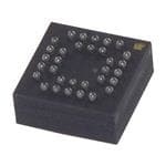
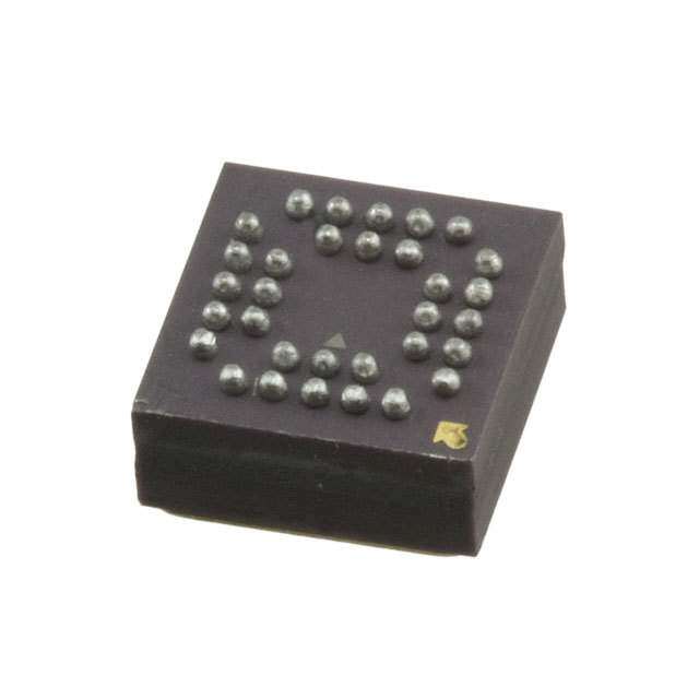
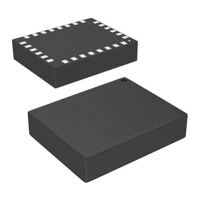
| 描述 | IC GYROSCOPE YAW RATE 32-CBGA螺旋仪 300 Deg/s Yaw Rate |
| 产品分类 | 陀螺仪运动与定位传感器 |
| 品牌 | Analog Devices Inc |
| 产品手册 | |
| 产品图片 |
|
| rohs | RoHS 合规性豁免无铅 / 不符合限制有害物质指令(RoHS)规范要求 |
| 产品系列 | 螺旋仪,Analog Devices ADXRS620BBGZ- |
| 数据手册 | |
| 产品型号 | ADXRS620BBGZ |
| PCN组件/产地 | |
| 产品种类 | 螺旋仪 |
| 传感轴 | Z |
| 供应商器件封装 | 32-CBGA(7x7) |
| 典型带宽 | 2.5kHz |
| 加速 | 2000 g |
| 商标 | Analog Devices |
| 宽度 | 7 mm |
| 封装 | Bulk |
| 封装/外壳 | 32-BFCBGA |
| 封装/箱体 | CBGA-32 |
| 工作温度 | -40°C ~ 105°C |
| 工厂包装数量 | 20 |
| 带宽 | 2500 Hz |
| 数字输出-位数 | - |
| 数字输出-总线接口 | - |
| 最大工作温度 | + 105 C |
| 最小工作温度 | - 40 C |
| 标准包装 | 1 |
| 灵敏度 | 6mV/°/s |
| 电压-电源 | 4.75 V ~ 5.25 V |
| 电流-电源 | 3.5mA |
| 电源电压-最大 | 5.25 V |
| 电源电压-最小 | 4.75 V |
| 电源电流 | 3.5 mA |
| 系列 | ADXRS620 |
| 范围 | +/- 300 deg/s |
| 范围°/s | ±300°/s |
| 输出类型 | 模拟 |
| 长度 | 7 mm |
| 高度 | 3 mm |


- 商务部:美国ITC正式对集成电路等产品启动337调查
- 曝三星4nm工艺存在良率问题 高通将骁龙8 Gen1或转产台积电
- 太阳诱电将投资9.5亿元在常州建新厂生产MLCC 预计2023年完工
- 英特尔发布欧洲新工厂建设计划 深化IDM 2.0 战略
- 台积电先进制程称霸业界 有大客户加持明年业绩稳了
- 达到5530亿美元!SIA预计今年全球半导体销售额将创下新高
- 英特尔拟将自动驾驶子公司Mobileye上市 估值或超500亿美元
- 三星加码芯片和SET,合并消费电子和移动部门,撤换高东真等 CEO
- 三星电子宣布重大人事变动 还合并消费电子和移动部门
- 海关总署:前11个月进口集成电路产品价值2.52万亿元 增长14.8%

PDF Datasheet 数据手册内容提取
±300°/sec Yaw Rate Gyro ADXRS620 FEATURES GENERAL DESCRIPTION Qualified for automotive applications The ADXRS620 is a complete angular rate sensor (gyroscope) Complete rate gyroscope on a single chip that uses the Analog Devices, Inc., surface-micromachining Z-axis (yaw rate) response process to create a functionally complete and low cost angular High vibration rejection over wide frequency rate sensor integrated with all required electronics on one chip. 2000 g powered shock survivability The manufacturing technique for this device is the same high Ratiometric to referenced supply volume BiMOS process that is used for high reliability automotive 5 V single-supply operation airbag accelerometers. 105°C operation Self-test on digital command The ADXRS620 is an automotive grade gyroscope that is 100% Ultrasmall and light (<0.15 cc, <0.5 gram) pin, package, temperature, and function compatible to the Temperature sensor output available industrial grade ADXRS652 gyro. Automotive grade RoHS compliant gyroscopes have more extensive guaranteed minimum/maximum specifications due to automotive testing. APPLICATIONS Vehicle chassis rollover sensing The output signal, RATEOUT (1B, 2A), is a voltage that is Inertial measurement units proportional to angular rate about the axis normal to the top Platform stabilization surface of the package. The output is ratiometric with respect to a provided reference supply. An external capacitor sets the bandwidth. Other external capacitors are required for operation. A temperature output is provided for compensation techniques. Two digital self-test inputs electromechanically excite the sensor to test proper operation of both the sensor and the signal condi- tioning circuits. The ADXRS620 is available in a 7 mm × 7 mm × 3 mm BGA ceramic package. FUNCTIONAL BLOCK DIAGRAM +5V (ADC REF) 100nF +5V AVCC ST2 ST1 TEMP VRATIO ADXRS620 100nF SELF-TEST 25kΩ 25kΩ @ 25°C AGND DEMOD DARMIVPE MESCEHNASNOICRAL AAMCP VGA +5V 180kΩ ±1% VDD CHARGE PUMP AND VOLTAGE 100nF REGULATOR PGND CP1 CP2 CP3 CP4 CP5 SUMJ RATEOUT 22nF 22nF 100nF COUT 08887-001 Figure 1. Rev. B Information furnished by Analog Devices is believed to be accurate and reliable. However, no responsibility is assumed by Analog Devices for its use, nor for any infringements of patents or other One Technology Way, P.O. Box 9106, Norwood, MA 02062-9106, U.S.A. rights of third parties that may result from its use. Specifications subject to change without notice. No license is granted by implication or otherwise under any patent or patent rights of Analog Devices. Tel: 781.329.4700 www.analog.com Trademarks and registered trademarks are the property of their respective owners. Fax: 781.461.3113 ©2010 Analog Devices, Inc. All rights reserved.
ADXRS620 TABLE OF CONTENTS Features .............................................................................................. 1 Setting Bandwidth .........................................................................9 Applications ....................................................................................... 1 Temperature Output and Calibration .........................................9 General Description ......................................................................... 1 Calibrated Performance ................................................................9 Functional Block Diagram .............................................................. 1 ADXRS620 and Supply Ratiometricity ................................... 10 Revision History ............................................................................... 2 Null Adjustment ......................................................................... 10 Specifications ..................................................................................... 3 Self-Test Function ...................................................................... 10 Absolute Maximum Ratings ............................................................ 4 Continuous Self-Test .................................................................. 10 Rate Sensitive Axis ....................................................................... 4 Outline Dimensions ....................................................................... 11 ESD Caution .................................................................................. 4 Ordering Guide .......................................................................... 11 Pin Configuration and Function Descriptions ............................. 5 Automotive Products ................................................................. 11 Typical Performance Characteristics ............................................. 6 Theory of Operation ........................................................................ 9 REVISION HISTORY 9/10—Rev. A to Rev. B Changes to Ordering Guide .......................................................... 11 7/10—Rev. 0 to Rev. A Changes to Features Section and General Description Section . 1 Added Note 2 to Ordering Guide ................................................. 11 Added Automotive Products Section........................................... 11 3/10—Revision 0: Initial Version Rev. B | Page 2 of 12
ADXRS620 SPECIFICATIONS All minimum and maximum specifications are guaranteed. Typical specifications are not guaranteed. T = −40°C to +105°C, V = AV = A S CC V = 5 V, V = AV , angular rate = 0°/sec, bandwidth = 80 Hz (C = 0.01 µF), I = 100 μA, ±1 g, unless otherwise noted. DD RATIO CC OUT OUT Table 1. Parameter Conditions Min Typ Max Unit SENSITIVITY1 Clockwise rotation is positive output Measurement Range2 Full-scale range over specifications range ±300 °/sec Initial and Over Temperature −40°C to +105°C 5.52 6 6.48 mV/°/sec Temperature Drift3 ±2 % Nonlinearity Best fit straight line 0.1 % of FS NULL1 Null −40°C to +105°C 2.2 2.5 2.8 V Linear Acceleration Effect Any axis 0.1 °/sec/g NOISE PERFORMANCE Rate Noise Density T ≤ 25°C 0.05 °/sec/√Hz A FREQUENCY RESPONSE Bandwidth4 0.01 2500 Hz Sensor Resonant Frequency 12 14.5 17 kHz SELF-TEST1 ST1 RATEOUT Response ST1 pin from Logic 0 to Logic 1 −650 −450 −250 mV ST2 RATEOUT Response ST2 pin from Logic 0 to Logic 1 250 450 650 mV ST1 to ST2 Mismatch5 −5 +5 % Logic 1 Input Voltage 3.3 V Logic 0 Input Voltage 1.7 V Input Impedance To common 40 50 100 kΩ TEMPERATURE SENSOR1 V at 25°C Load = 10 MΩ 2.35 2.5 2.65 V OUT Scale Factor6 @ 25°C, V = 5 V 9 mV/°C RATIO Load to V 25 kΩ S Load to Common 25 kΩ TURN-ON TIME Power on to ±½°/sec of final 50 ms OUTPUT DRIVE CAPABILITY Current Drive For rated specifications 200 µA Capacitive Load Drive 1000 pF POWER SUPPLY Operating Voltage (V) 4.75 5.00 5.25 V S Quiescent Supply Current 3.5 4.5 mA TEMPERATURE RANGE Specified Performance −40 +105 °C 1 Parameter is linearly ratiometric with V . RATIO 2 The maximum range possible, including output swing range, initial offset, sensitivity, offset drift, and sensitivity drift at 5 V supplies. 3 From +25°C to −40°C or from +25°C to 105°C. 4 Adjusted by external capacitor, C . Reducing bandwidth below 0.01 Hz does not reduce noise further. OUT 5 Self-test mismatch is described as (ST2 + ST1)/((ST2 − ST1)/2). 6 For a change in temperature from 25°C to 26°C. V is ratiometric to V . See the Temperature Output and Calibration section for more details. TEMP RATIO Rev. B | Page 3 of 12
ADXRS620 ABSOLUTE MAXIMUM RATINGS RATE SENSITIVE AXIS Table 2. Parameter Rating The ADXRS620 is a Z-axis rate-sensing device (also called Acceleration (Any Axis, 0.5 ms) a yaw rate sensing device). It produces a positive going output Unpowered 2000 g voltage for clockwise rotation about the axis normal to the Powered 2000 g package top, that is, clockwise when looking down at the V , AV −0.3 V to +6.0 V package lid. DD CC V AV RATIO CC RATE RATE OUT ST1, ST2 AV AXIS CC VCC = 5V Output Short-Circuit Duration Indefinite LONGITUDINAL 4.75V (Any Pin to Common) AXIS + 7 VRATIO/2 Operating Temperature Range −55°C to +125°C RATE IN Storage Temperature Range −65°C to +150°C A1 LAATBECRADLE AFXIGS1 GND 0.25V 08887-002 Stresses above those listed under the Absolute Maximum Figure 2. RATEOUT Signal Increases with Clockwise Rotation Ratings may cause permanent damage to the device. This is a stress rating only; functional operation of the device at these or ESD CAUTION any other conditions above those indicated in the operational section of this specification is not implied. Exposure to absolute maximum rating conditions for extended periods may affect device reliability. Drops onto hard surfaces can cause shocks of greater than 2000 g and can exceed the absolute maximum rating of the device. Exercise care during handling to avoid damage. Rev. B | Page 4 of 12
ADXRS620 PIN CONFIGURATION AND FUNCTION DESCRIPTIONS PGND VDD CP5 CP3 CP4 7 6 ST1 CP1 5 ST2 CP2 4 TEMP AVCC 3 2 1 AGND RATEOUT G F VRAETIO NDC SUCMJ B A 08887-003 Figure 3. Pin Configuration Table 3. Pin Function Descriptions Pin No. Mnemonic Description 6D, 7D CP5 HV Filter Capacitor (0.1 µF) 6A, 7B CP4 Charge Pump Capacitor (22 nF) 6C, 7C CP3 Charge Pump Capacitor (22 nF) 5A, 5B CP1 Charge Pump Capacitor (22 nF) 4A, 4B CP2 Charge Pump Capacitor (22 nF) 3A, 3B AV Positive Analog Supply CC 1B, 2A RATEOUT Rate Signal Output 1C, 2C SUMJ Output Amp Summing Junction 1D, 2D NC No Connect 1E, 2E V Reference Supply for Ratiometric Output RATIO 1F, 2G AGND Analog Supply Return 3F, 3G TEMP Temperature Voltage Output 4F, 4G ST2 Self-Test for Sensor 2 5F, 5G ST1 Self-Test for Sensor 1 6G, 7F PGND Charge Pump Supply Return 6E, 7E V Positive Charge Pump Supply DD Rev. B | Page 5 of 12
ADXRS620 TYPICAL PERFORMANCE CHARACTERISTICS N > 1000 for all typical performance plots, unless otherwise noted. 20 30 18 %) %) 25 N ( 16 N ( O O ATI 14 ATI 20 PUL 12 PUL O O OF P 10 OF P 15 GE 8 GE NTA 6 NTA 10 CE CE PER 4 PER 5 2 0 2.20 2.25 2.30 2.35 2.40 RA2.45TE O2.50UT (2.55V) 2.60 2.65 2.70 2.75 2.80 08887-004 0–10 –8 –6 –4 –2DRIF0T (%)2 4 6 8 10 08887-007 Figure 4. Null Output at 25°C (V = 5 V) Figure 7. Sensitivity Drift over Temperature RATIO 45 35 40 %) %) 30 N ( 35 N ( O O TI TI 25 A 30 A L L U U OP 25 OP 20 P P F F E O 20 E O 15 G G A A T 15 T EN EN 10 RC 10 RC E E P P 5 5 0–0.5 –0.4 –0.3 –0.2 –0.1(°/se0c°/C)0.1 0.2 0.3 0.4 0.5 08887-005 0–650 –610 –570 –530 –49S0T–14 Δ50 (m–V4)10 –370 –330 –290 –250 08887-008 Figure 5. Null Drift over Temperature (V = 5 V) Figure 8. ST1 Output Change at 25°C (V = 5 V) RATIO RATIO 16 40 14 35 %) 12 ON ( 30 ATION 10 PULATI 25 L O OPU 8 OF P 20 % OF P 6 TAGE 15 N 4 CE 10 R E P 2 5 0 5.5 5.6 5.7 5.S8ENS5.I9TIVIT6Y (mV6./1°/sec6).2 6.3 6.4 6.5 08887-006 0250 290 330 370 41S0T24 Δ5 0(mV4)90 530 570 610 650 08887-009 Figure 6. Sensitivity at 25°C (V = 5 V) Figure 9. ST2 Output Change at 25°C (V = 5 V) RATIO RATIO Rev. B | Page 6 of 12
ADXRS620 70 40 %) 60 %) 35 N ( N ( O O 30 TI 50 TI A A UL UL 25 OP 40 OP P P F F 20 O O E 30 E G G 15 A A T T N 20 N CE CE 10 R R E E P 10 P 5 0 –5 –4 –3 S–2ELF-–T1EST M0ISMA1TCH (2%) 3 4 5 08887-010 02.40 2.42 2.44 2.46 2.V48OLT2.A5G0E 2(V.5)2 2.54 2.56 2.58 2.60 08887-015 Figure 10. Self-Test Mismatch at 25°C (V = 5 V) Figure 13. V Output at 25°C (V = 5 V) RATIO TEMP RATIO 600 3.3 3.1 400 ST2 2.9 V) 200 2.7 Δ (m E (V) 2.5 T G F-TES 0 OLTA 2.3 L V SE –200 2.1 1.9 –400 ST1 1.7 256 PARTS –600 1.5 –40 –20 0 TE2M0PERA4T0URE (°6C0) 80 100 120 08887-011 –40 –20 0 T2E0MPERA40TURE (6°0C) 80 100 120 08887-013 Figure 11. Typical Self-Test Change over Temperature Figure 14. V Output over Temperature (V = 5 V) TEMP RATIO 30 60 REF %)25 50 Y N ( X O 40 +45° TI A20 –45° UL 30 OP sec F P15 R °/ 20 O O E g G 10 TA10 N CE 0 R PE 5 –10 0 –20 2.5 2.7 2.9CUR3R.E1NT 3C.3ONS3U.5MPT3IO.7N (m3.A9) 4.1 4.3 4.5 08887-012 750 770 790TIME (ms)810 830 850 08887-014 Figure 12. Current Consumption at 25°C (V = 5 V) Figure 15. g and g × g Sensitivity for a 50 g, 10 ms Pulse RATIO Rev. B | Page 7 of 12
ADXRS620 2.0 0.10 LAT 1.8 LONG RATE 1.6 c)0.05 e ATEOUT (°/s) 111...240 OTATION (°/s 0 R R AK 0.8 OF E E P 0.6 T RA–0.05 0.4 0.2 0100 FREQUE1NkCY (Hz) 10k 08887-116 –0.100 20 40 T6IM0E (Hou8r0s) 100 120 140 08887-018 Figure 16. Typical Response to 10 g Sinusoidal Vibration Figure 19. Typical Shift in 90 sec Null Averages Accumulated (Sensor Bandwidth = 2 kHz) over 140 Hours 400 0.10 300 DUT1 OFFSET BY +200°/sec ON (°/sec) 210000 ON (°/sec)0.05 ATI ATI OT 0 OT 0 R R OF –100 OF E E RAT–200 DUT2 OFFSET BY –200°/sec RAT–0.05 –300 –4000 50 100TIME (ms)150 200 250 08887-016 –0.100 600 1200TIME 1(S8e0c0onds)2400 3000 3600 08887-019 Figure 17. Typical High g (2500 g) Shock Response Figure 20. Typical Shift in Short-Term Null (Bandwidth = 1 Hz) (Sensor Bandwidth = 40 Hz) 1 0.1 s) m ec rms) c/√Hz r ON (°/s 0.1 TY(°/se 0.01 TI SI A N EVI DE D L AN RA ALL0.01 ECT0.001 ROOT OISE SP N 0.0010.01 0.1 1AVERAG10E TIME 1(0S0econds1)k 10k 100k 08887-017 0.000110 100 FREQUE1NkCY (Hz) 10k 100k 08887-020 Figure 18. Typical Root Allan Deviation at 25°C vs. Averaging Time Figure 21. Typical Noise Spectral Density (Bandwidth = 40 Hz) Rev. B | Page 8 of 12
ADXRS620 THEORY OF OPERATION The ADXRS620 operates on the principle of a resonator gyro. Figure 22 shows the effect of adding a 250 Hz filter to the output Two polysilicon sensing structures each contain a dither frame of an ADXRS620 set to 40 Hz bandwidth (as shown in Figure 21). that is electrostatically driven to resonance, producing the High frequency demodulation artifacts are attenuated by necessary velocity element to produce a Coriolis force during approximately 18 dB. angular rate. At two of the outer extremes of each frame, 0.1 orthogonal to the dither motion, are movable fingers that are s) placed between fixed pickoff fingers to form a capacitive pickoff m structure that senses Coriolis motion. The resulting signal is fed Hz r 0.01 √ c/ to a series of gain and demodulation stages that produces the se electrical rate signal output. The dual-sensor design rejects TY(°/ 0.001 external g-forces and vibration. Fabricating the sensor with the NSI E signal conditioning electronics preserves signal integrity in L D A0.0001 noisy environments. R T C E P The electrostatic resonator requires 18 V to 20 V for operation. S E 0.00001 S Because only 5 V are typically available in most applications, OI N a charge pump is included on chip. If an external 18 V to 20 V 0.000001 sbuep opmlyi titse adv aanildab tlhei,s t hsuep tpwloy ccaanpa bceit coorsn nonec CtePd1 t oth CroPu5g (hP CinP 64D c,a n 10 100 FREQUE1NkCY (Hz) 10k 100k 08887-021 Pin 7D). Note that CP5 should not be grounded when power is Figure 22. Noise Spectral Density with Additional 250 Hz Filter applied to the ADXRS620. Although no damage occurs, under TEMPERATURE OUTPUT AND CALIBRATION certain conditions the charge pump may fail to start up after the ground is removed without first removing power from the It is common practice to temperature-calibrate gyros to improve ADXRS620. their overall accuracy. The ADXRS620 has a temperature propor- tional voltage output that provides input to such a calibration SETTING BANDWIDTH method. The temperature sensor structure is shown in Figure 23. External Capacitor C is used in combination with the on- The temperature output is characteristically nonlinear, and any OUT chip R resistor to create a low-pass filter to limit the load resistance connected to the TEMP output results in decreasing OUT bandwidth of the ADXRS620 rate response. The −3 dB the TEMP output and temperature coefficient. Therefore, buf- frequency set by R and C is fering the output is recommended. OUT OUT f = ( 1 ) The voltage at the TEMP pin (3F, 3G) is nominally 2.5 V at 25°C, OUT 2×π×R ×C and V = 5 V. The temperature coefficient is ~9 mV/°C at OUT OUT RATIO 25°C. Although the TEMP output is highly repeatable, it has This frequency can be well controlled because R has been OUT only modest absolute accuracy. trimmed during manufacturing to be 180 kΩ ± 1%. Any external resistor applied between the RATEOUT pin (1B, 2A) VRATIO VTEMP and SUMJ pin(1 (810Ck, Ω2C×)R resu)lts in RFIXED RTEMP 08887-022 R = ( EXT) Figure 23. Temperature Sensor Structure OUT 180kΩ+R EXT CALIBRATED PERFORMANCE In general, an additional hardware or software filter is added Using a three-point calibration technique, it is possible to to attenuate high frequency noise arising from demodulation calibrate the null and sensitivity drift of the ADXRS620 to spikes at the gyro’s 14 kHz resonant frequency. (The noise spikes an overall accuracy of nearly 200°/hour. An overall accuracy at 14 kHz can be clearly seen in the power spectral density curve of 40°/hour or better is possible using more points. shown in Figure 21). Typically, this additional filter’s corner frequency is set to greater than 5× the required bandwidth to Limiting the bandwidth of the device reduces the flat-band preserve good phase response. noise during the calibration process, improving the measure- ment accuracy at each calibration point. Rev. B | Page 9 of 12
ADXRS620 ADXRS620 AND SUPPLY RATIOMETRICITY NULL ADJUSTMENT The ADXRS620 RATEOUT and TEMP signals are ratiometric The nominal 2.5 V null is for a symmetrical swing range at to the VRATIO voltage, that is, the null voltage, rate sensitivity, and RATEOUT (1B, 2A). However, a nonsymmetrical output swing temperature outputs are proportional to VRATIO. Thus, the may be suitable in some applications. Null adjustment is possible ADXRS620 is most easily used with a supply-ratiometric ADC by injecting a suitable current to SUMJ (1C, 2C). Note that supply that results in self-cancellation of errors due to minor supply disturbances may reflect some null instability. Digital supply variations. There is some small error due to nonratiometric noise should be avoided, particularly in this case. behavior. Typical ratiometricity error for null, sensitivity, self- SELF-TEST FUNCTION test, and temperature output is outlined in Table 4. The ADXRS620 includes a self-test feature that actuates each of Note that V must never be greater than AV RATIO CC. the sensing structures and associated electronics as if subjected to angular rate. It is activated by standard logic high levels applied Table 4. Ratiometricity Error for Various Parameters to Input ST1 (5F, 5G), Input ST2 (4F, 4G), or both. ST1 causes Parameter V = V = 4.85 V V = V = 5.15 V S RATIO S RATIO the voltage at RATEOUT to change about −0.450 V, and ST2 ST1 causes an opposite change of +0.450 V. The self-test response Mean 0.3% 0.09% follows the viscosity temperature dependence of the package Sigma 0.21% 0.19% atmosphere, approximately 0.25%/°C. ST2 Mean −0.15% −0.2% Activating both ST1 and ST2 simultaneously is not damaging. Sigma 0.22% 0.2% ST1 and ST2 are fairly closely matched (±5%), but actuating Null both simultaneously may result in a small apparent null bias Mean −0.3% −0.05% shift proportional to the degree of self-test mismatch. Sigma 0.2% 0.08% ST1 and ST2 are activated by applying a voltage equal to V Sensitivity RATIO to the ST1 and ST2 pins. The voltage applied to ST1 and ST2 Mean 0.003% −0.25% must never be greater than AV . Sigma 0.06% 0.06% CC V CONTINUOUS SELF-TEST TEMP Mean −0.2% −0.04% The on-chip integration of the ADXRS620 gives it higher reliability Sigma 0.05% 0.06% than is obtainable with any other high volume manufacturing method. In addition, it is manufactured under a mature BiMOS process with field-proven reliability. As an additional failure detection measure, a power-on self-test can be performed. However, some applications may warrant continuous self-test while sensing rate. Details outlining continuous self-test techniques are also available in the AN-768 Application Note at analog.com. Rev. B | Page 10 of 12
ADXRS620 OUTLINE DIMENSIONS 7.05 A1BALL 6.85SQ *IAN1DCEOXRANREERA CORNER 6.70 7 6 5 4 3 2 1 A B 4.80 BSCSQ C 0.80 D BSC E F G TOPVIEW BOTTOMVIEW DETAILA 3.80MAX DETAILA 3.20MAX 0.60MAX 2.50MIN 0.25MIN 0.60 COPLANARITY SEATING 0.55 0.15 PLANE 0.50 *BTAOLTLHAE1DID/AEPNATIDFIIENRTEISRNGAOLLLDYPVLIAATHEODBLAEANSLD.LDCIOANMNEETCETRED 10-26-2009-B Figure 24. 32-Lead Ceramic Ball Grid Array [CBGA] (BG-32-3) Dimensions shown in millimeters ORDERING GUIDE Model1, 2 Temperature Range Package Description Package Option ADXRS620BBGZ –40°C to +105°C 32-Lead Ceramic Ball Grid Array (CBGA) BG-32-3 ADXRS620BBGZ-RL –40°C to +105°C 32-Lead Ceramic Ball Grid Array (CBGA) BG-32-3 ADXRS620WBBGZA –40°C to +105°C 32-Lead Ceramic Ball Grid Array (CBGA) BG-32-3 ADXRS620WBBGZA-RL –40°C to +105°C 32-Lead Ceramic Ball Grid Array (CBGA) BG-32-3 EVAL-ADXRS620Z Evaluation Board 1 Z = RoHS Compliant Part. 2 W = Qualified for Automotive Applications. AUTOMOTIVE PRODUCTS The ADXRS620W models are available with controlled manufacturing to support the quality and reliability requirements of automotive applications. Note that these automotive models may have specifications that differ from the commercial models; therefore, designers should review the Specifications section of this data sheet carefully. Only the automotive grade products shown are available for use in automotive applications. Contact your local Analog Devices account representative for specific product ordering information and to obtain the specific Automotive Reliability reports for these models. Rev. B | Page 11 of 12
ADXRS620 NOTES ©2010 Analog Devices, Inc. All rights reserved. Trademarks and registered trademarks are the property of their respective owners. D08887-0-9/10(B) Rev. B | Page 12 of 12
Mouser Electronics Authorized Distributor Click to View Pricing, Inventory, Delivery & Lifecycle Information: A nalog Devices Inc.: EVAL-ADXRS620Z ADXRS620BBGZ ADXRS620BBGZ-RL