ICGOO在线商城 > 传感器,变送器 > 运动传感器 - 陀螺仪 > MPU-3050
 Datasheet下载
- 型号: MPU-3050
- 制造商: Invensense
- 库位|库存: xxxx|xxxx
- 要求:
| 数量阶梯 | 香港交货 | 国内含税 |
| +xxxx | $xxxx | ¥xxxx |
查看当月历史价格
查看今年历史价格
MPU-3050产品简介:
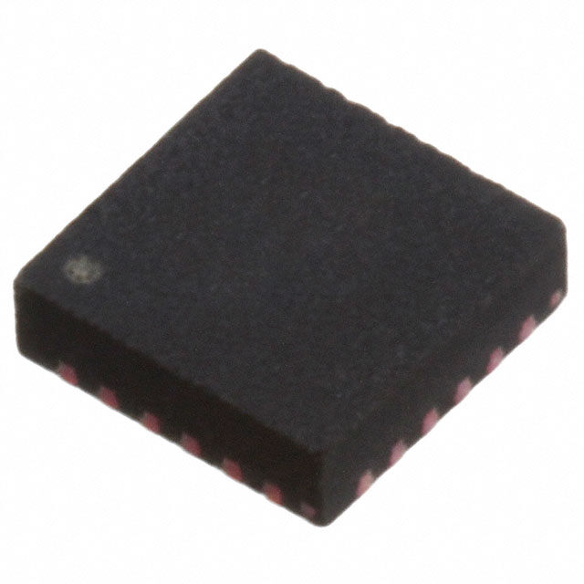
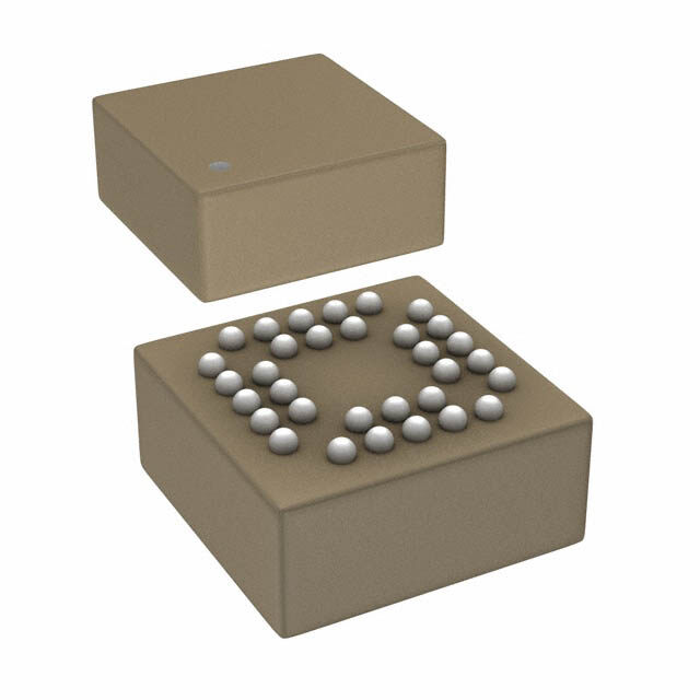
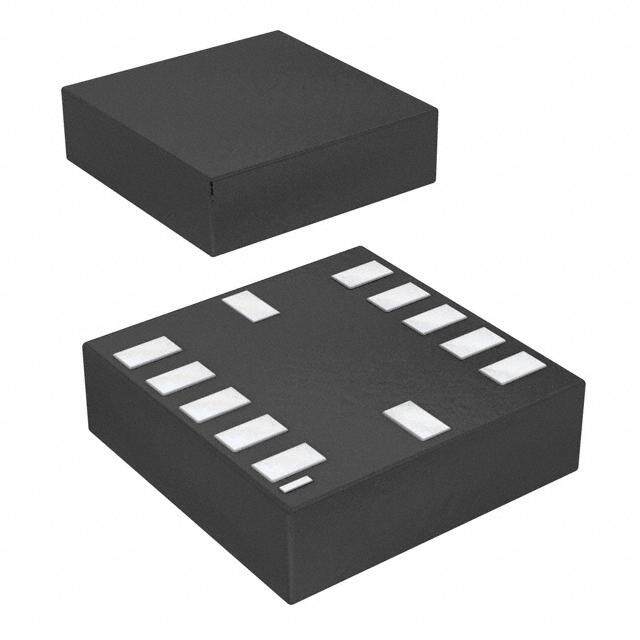
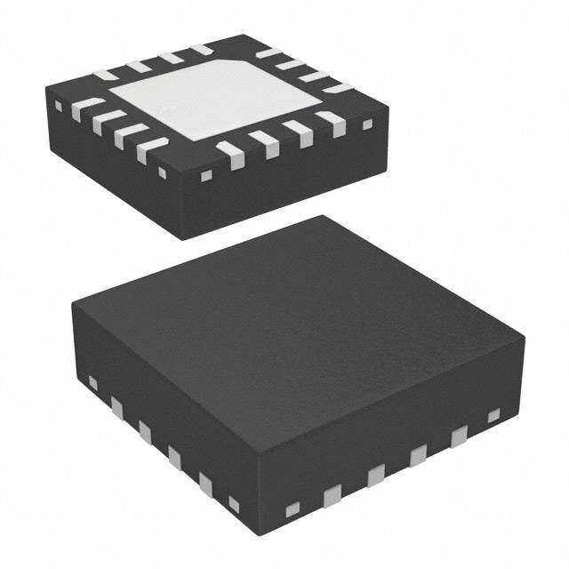
ICGOO电子元器件商城为您提供MPU-3050由Invensense设计生产,在icgoo商城现货销售,并且可以通过原厂、代理商等渠道进行代购。 MPU-3050价格参考¥37.77-¥103.86。InvensenseMPU-3050封装/规格:运动传感器 - 陀螺仪, Gyroscope X (Pitch), Y (Roll), Z (Yaw) ±250, 500, 1000, 2000 33kHz (X), 30kHz (Y), 27kHz (Z) I²C 24-QFN (4x4)。您可以下载MPU-3050参考资料、Datasheet数据手册功能说明书,资料中有MPU-3050 详细功能的应用电路图电压和使用方法及教程。
TDK InvenSense MPU-3050 是一款三轴陀螺仪传感器,广泛应用于多种运动传感和姿态控制的场景中。以下是该型号的一些典型应用场景:

1. 消费电子产品:
   - 智能手机和平板电脑:MPU-3050 可用于检测设备的旋转和倾斜角度,从而实现屏幕自动旋转、游戏控制等功能。
   - 可穿戴设备:如智能手表和健身追踪器,可以监测用户的动作和姿态,提供步数统计、运动模式识别等健康监测功能。

2. 无人机和航模:
   - 飞行姿态控制:通过实时监测无人机或航模的姿态变化,帮助稳定飞行,防止翻滚和失控,提高飞行安全性和稳定性。

3. 智能家居:
   - 智能安防系统:可以用于门窗传感器,检测异常开合动作,触发报警;也可以用于智能摄像头,根据移动物体的方向调整拍摄角度。
   - 智能家电:如扫地机器人,利用陀螺仪数据进行导航和路径规划,确保清洁覆盖范围最大化。

4. 汽车电子:
   - 车身稳定控制系统(ESC):通过检测车辆的侧倾和俯仰角度,辅助驾驶员保持车辆稳定,避免侧滑和翻车风险。
   - 气囊控制系统:在碰撞发生时,准确判断车辆的旋转状态,确保气囊及时展开,保护乘员安全。

5. 工业自动化:
   - 机器人手臂控制:精确测量机械臂的转动角度,实现高精度的操作和定位,适用于装配线、物流搬运等场景。
   - 振动监测:对机械设备的振动情况进行实时监控,预测故障并进行预防性维护,延长设备使用寿命。

6. 虚拟现实(VR)和增强现实(AR):
   - 头戴式显示器(HMD):捕捉用户头部的细微动作,提供沉浸式的视觉体验,使虚拟环境更加逼真自然。

总之,TDK InvenSense MPU-3050 凭借其高精度、低功耗和小尺寸的特点,适用于各种需要精确运动感知的应用领域,为设备提供了更智能、更稳定的性能表现。
| 参数 | 数值 |
| 产品目录 | |
| 描述 | GYRO/ACCELEROMETER 3-AXIS 24QFN |
| 产品分类 | 陀螺仪 |
| 品牌 | InvenSense |
| 数据手册 | |
| 产品图片 |
|
| 产品型号 | MPU-3050 |
| rohs | 无铅 / 符合限制有害物质指令(RoHS)规范要求 |
| 产品系列 | Motion Processing Unit™ |
| 传感器类型 | Motion Processing Unit™ |
| 供应商器件封装 | * |
| 其它名称 | 1428-1001-2 |
| 典型带宽 | 30kHz |
| 封装/外壳 | 24-QFN |
| 工作温度 | -40°C ~ 105°C |
| 标准包装 | 5,000 |
| 灵敏度 | 131LSB/(°/s), 65.5LSB/(°/s), 32.8LSB/(°/s), 16.4LSB/(°/s) |
| 特色产品 | http://www.digikey.com/product-highlights/cn/zh/invensense-mpu-3050/3808 |
| 电压-电源 | 2.1V ~ 3.6V |
| 电流-电源 | 5.9mA |
| 范围°/s | ±250°/s, ±500°/s, ±1000°/s, ±2000°/s |
| 输出类型 | I²C |


- 商务部:美国ITC正式对集成电路等产品启动337调查
- 曝三星4nm工艺存在良率问题 高通将骁龙8 Gen1或转产台积电
- 太阳诱电将投资9.5亿元在常州建新厂生产MLCC 预计2023年完工
- 英特尔发布欧洲新工厂建设计划 深化IDM 2.0 战略
- 台积电先进制程称霸业界 有大客户加持明年业绩稳了
- 达到5530亿美元!SIA预计今年全球半导体销售额将创下新高
- 英特尔拟将自动驾驶子公司Mobileye上市 估值或超500亿美元
- 三星加码芯片和SET,合并消费电子和移动部门,撤换高东真等 CEO
- 三星电子宣布重大人事变动 还合并消费电子和移动部门
- 海关总署:前11个月进口集成电路产品价值2.52万亿元 增长14.8%

PDF Datasheet 数据手册内容提取
MPU-3050 MPU-3050 Motion Processing Unit Product Specification InvenSense reserves the right to change the InvenSense Inc. Document Number: PS-MPU-3050A-00 detail specifications as may be required to 1745 Technology Drive, San Jose, CA 95110 U.S.A Revision: 2.7 permit improvements in the design of its +1(408) 988–7339 Rev. Date: 03/10/2016 products. www.invensense.com
MPU-3050 TABLE OF CONTENTS 1 INTRODUCTION.................................................................................................................................................... 4 1.1 PURPOSE AND SCOPE ............................................................................................................................................... 4 1.2 PRODUCT OVERVIEW ............................................................................................................................................... 4 1.3 APPLICATIONS ......................................................................................................................................................... 5 2 FEATURES ............................................................................................................................................................ 6 2.1 SENSORS ................................................................................................................................................................ 6 2.2 DIGITAL OUTPUT ..................................................................................................................................................... 6 2.3 MOTION PROCESSING .............................................................................................................................................. 6 2.4 CLOCKING .............................................................................................................................................................. 6 2.5 POWER .................................................................................................................................................................. 6 2.6 PACKAGE ............................................................................................................................................................... 7 3 ELECTRICAL CHARACTERISTICS ............................................................................................................................. 8 3.1 SENSOR SPECIFICATIONS ........................................................................................................................................... 8 3.2 ELECTRICAL SPECIFICATIONS....................................................................................................................................... 9 3.3 ELECTRICAL SPECIFICATIONS, CONTINUED ................................................................................................................... 10 3.4 ELECTRICAL SPECIFICATIONS, CONTINUED ................................................................................................................... 11 3.5 I2C TIMING CHARACTERIZATION ............................................................................................................................... 12 3.6 ABSOLUTE MAXIMUM RATINGS ............................................................................................................................... 13 4 APPLICATIONS INFORMATION ........................................................................................................................... 14 4.1 PIN OUT AND SIGNAL DESCRIPTION .......................................................................................................................... 14 4.2 TYPICAL OPERATING CIRCUITS .................................................................................................................................. 15 4.3 BILL OF MATERIALS FOR EXTERNAL COMPONENTS ....................................................................................................... 15 4.4 RECOMMENDED POWER-ON PROCEDURE................................................................................................................... 16 5 FUNCTIONAL OVERVIEW .................................................................................................................................... 17 5.1 BLOCK DIAGRAM ................................................................................................................................................... 17 5.2 OVERVIEW ........................................................................................................................................................... 17 5.3 THREE-AXIS MEMS GYROSCOPE WITH 16-BIT ADCS AND SIGNAL CONDITIONING ............................................................ 17 5.4 DIGITAL MOTION PROCESSOR .................................................................................................................................. 18 5.5 PRIMARY I2C SERIAL COMMUNICATIONS INTERFACE ..................................................................................................... 18 5.6 SECONDARY I2C SERIAL INTERFACE (FOR A THIRD-PARTY ACCELEROMETER) ....................................................................... 18 6 CLOCKING .......................................................................................................................................................... 19 6.1 INTERNAL CLOCK GENERATION ................................................................................................................................. 19 6.2 CLOCK OUTPUT ..................................................................................................................................................... 19 6.3 SENSOR DATA REGISTERS ........................................................................................................................................ 19 6.4 FIFO ................................................................................................................................................................... 19 6.5 INTERRUPTS .......................................................................................................................................................... 19 6.6 BIAS AND LDO ...................................................................................................................................................... 20 6.7 CHARGE PUMP ...................................................................................................................................................... 20 6.8 CHIP VERSION ....................................................................................................................................................... 20 7 DIGITAL INTERFACE ............................................................................................................................................ 21 7.1 I2C SERIAL INTERFACE ............................................................................................................................................. 21 8 SERIAL INTERFACE CONSIDERATIONS (MPU-3050) ............................................................................................. 25 Rev Date: 03/10/2016 InvenSense Confidential & Proprietary Page 2 of 52 Document Number: PS-MPU-3050A-00 Revision: 2.7
MPU-3050 8.1 MPU-3050 SUPPORTED INTERFACES ....................................................................................................................... 25 8.2 LOGIC LEVELS ........................................................................................................................................................ 25 9 MOTION PROCESSING LIBRARY (MPL) ............................................................................................................... 28 9.1 DEMO SOFTWARE .................................................................................................................................................. 29 10 ASSEMBLY ...................................................................................................................................................... 29 10.1 ORIENTATION ....................................................................................................................................................... 29 10.2 PCB LAYOUT GUIDELINES ....................................................................................................................................... 30 10.3 TRACE ROUTING .................................................................................................................................................... 32 10.4 COMPONENT PLACEMENT ....................................................................................................................................... 32 10.5 PCB MOUNTING AND CROSS-AXIS SENSITIVITY ........................................................................................................... 33 10.6 PACKAGE MARKING SPECIFICATION ........................................................................................................................... 34 11 REGISTER MAP ............................................................................................................................................... 35 12 REGISTER DESCRIPTION .................................................................................................................................. 36 12.1 REGISTER 0 – WHO AM I ........................................................................................................................................ 36 12.2 REGISTER 01 – PRODUCT ID .................................................................................................................................... 37 12.3 REGISTERS 12 TO 17 – GYRO OFFSETS ...................................................................................................................... 38 12.4 REGISTER 18 – FIFO ENABLE ................................................................................................................................... 39 12.5 REGISTER 19 – AUX (ACCEL) VDDIO ....................................................................................................................... 39 12.6 REGISTER 20 – AUX (ACCEL) SLAVE ADDRESS ............................................................................................................ 40 12.7 REGISTER 21 – SAMPLE RATE DIVIDER....................................................................................................................... 40 12.8 REGISTER 22 – DLPF, FULL SCALE, EXTERNAL SYNC ..................................................................................................... 41 12.9 REGISTER 23 – INTERRUPT CONFIGURATION ............................................................................................................... 43 12.10 REGISTER 24 – AUX (ACCEL) BURST READ ADDRESS ............................................................................................... 43 12.11 REGISTER 26 – INTERRUPT STATUS ....................................................................................................................... 44 12.12 REGISTERS 27 TO 40 – SENSOR REGISTERS ............................................................................................................. 44 12.13 REGISTERS 58 TO 59 – FIFO COUNT ..................................................................................................................... 45 12.14 REGISTER 60 – FIFO DATA ................................................................................................................................. 45 12.15 REGISTER 61 – USER CONTROL ............................................................................................................................ 47 12.16 REGISTER 62 – POWER MANAGEMENT.................................................................................................................. 47 13 REFERENCE ..................................................................................................................................................... 49 14 REVISION HISTORY ......................................................................................................................................... 50 Rev Date: 03/10/2016 Page 3 of 52 Document Number: PS-MPU-3050A-00 Revision: 2.7
MPU-3050 1 Introduction 1.1 Purpose and Scope This document provides a description, specifications, and design-related information for the MPU-3050 Motion Processing Unit ®. References [1], [2] and [3] provide a complementary set of software guides for the Motion Processing Library (MPL) and describe in detail the API and System Layer routines needed for interfacing to the MPU-3050. Electrical characteristics are based upon simulation results and limited characterization data. Specifications are subject to change without notice. 1.2 Product Overview The MPU-3050 Motion Processing Unit (MPU) is the world’s first motion processing solution with integrated 6-axis sensor fusion for smartphone applications. The MPU-3050 has an embedded 3-axis gyroscope and Digital Motion Processor ® (DMP) hardware accelerator engine with a secondary I2C port that interfaces to third party digital accelerometers to deliver a complete 6-axis sensor fusion output to its primary I2C port. This combines both linear and rotational motion into a single data stream for the application. This breakthrough in gyroscope technology provides a dramatic 68% smaller footprint, 40% thinner package, consumes 55% less power, and has inherent cost advantages compared to the latest competitive gyro solutions to uniquely address the fast-growing demand for 6-axis motion processing in mobile handsets. The MPU-3050 significantly extends and transforms motion sensing features provided by accelerometers beyond portrait and landscape orientation, to motion processing functionality. The MPU measures and processes both linear and rotational movements, creating a higher degree of 1:1 motion interactivity between the user and their handset. Similar to the proliferation of Bluetooth, camera phone image sensors and Wi-Fi, motion processing is becoming a “must-have” function in mobile handsets benefitting wireless carriers, mobile handset OEMs, application developers and end-users. By providing an integrated sensor fusion output, the DMP in the MPU-3050 offloads the intensive motion processing computation requirements from the applications processor, reducing the need for frequent polling of the motion sensor output and enabling use of low-cost, low-power application processors, thereby increasing overall battery life of handsets. Since handsets today are of multi-function nature, MPU-3050 not only provides accurate 1:1 motion tracking for some of the more common applications such as still/video image stabilization, gaming and dead reckoning, the 32-bit DMP can be programmed to deliver advanced UI, e.g. multiple kinds of gestures and character recognition leading to applications such as Airsign ®, TouchAnywhere ®, MotionCommand ®. By leveraging its patented and volume-proven Nasiri-Fabrication platform, which integrates MEMS wafers with companion CMOS electronics through wafer-level bonding, InvenSense has driven the MPU-3050 package size down to a revolutionary footprint of 4x4x0.9mm (QFN), while providing the highest performance, lowest noise, and the lowest cost semiconductor packaging to address a wide range of handheld consumer electronic devices. The MPU-3050 integrates 16-bit analog-to-digital converters (ADCs), selectable low-pass filters, FIFO, embedded temperature sensor, and Fast Mode I2C interface. Performance features include programmable full-scale range from 250 degrees-per-second up to 2000 degrees-per-second (º/s or dps), and low-noise of 0.01º/s/√Hz, while providing the highest robustness supporting 10,000g shock in operation. The highest cross-axis isolation is achieved by design from its single silicon integration. Factory-calibrated initial sensitivity reduces production-line calibration requirements. The part’s on-chip FIFO and dedicated I2C-master accelerometer sensor bus simplifies system timing and lowers system power consumption. The sensor bus allows the MPU-3050 to directly acquire data from the off-chip Rev Date: 03/10/2016 Page 4 of 52 Document Number: PS-MPU-3050A-00 Revision: 2.7
MPU-3050 [1] MPL Programmer’s Guide – Application Note (AN-MPL-3000-UG-01 or later) [2] MPL Functional Specification (DOC-MPL-FS-V2.3 or later) [3] MPL Product Specification (PS-MPL-3000-v2.0 or later) accelerometer without intervention from an external processor. Other industry-leading features include a small 4 mm x 4 mm x 0.9 mm plastic QFN package, an embedded temperature sensor, programmable interrupts, and a low 13 mW power consumption. Parts are available with I2C serial interface, a VDD operating range of 2.1 V to 3.6 V, and a VLOGIC interface voltage from 1.71 V to 3.6 V. The MPU-3050 supports the I2C serial interface and has a separate VLOGIC reference pin (in addition to its analog supply pin, VDD), which sets the logic levels of its I2C interface. The VLOGIC voltage may be between 1.71 V min to VDD max. The table below outlines these details: Power Supply and supported interface for MPU-3050 Part / Item MPU-3050 VDD 2.1 V to 3.6 V VLOGIC 1.71 V to VDD Serial Interfaces Supported I2C Pin 8 VLOGIC Pin 9 AD0 Pin 23 SCL Pin 24 SDA 1.3 Applications • Handset gaming • Location-based services, points of interest, and dead reckoning • Improved camera image quality through image stabilization • Health and sports monitoring Rev Date: 03/10/2016 Page 5 of 52 Document Number: PS-MPU-3050A-00 Revision: 2.7
MPU-3050 2 Features The MPU-3050 Motion Processing Unit includes a wide range of features: 2.1 Sensors • X-, Y-, Z-Axis angular rate sensors (gyros) on one integrated circuit • Digital-output temperature sensor • External sync signal connected to the FSYNC pin supports image, video and GPS synchronization • 6-axis motion processing capability using secondary I2C interface to directly connect to a digital 3-axis third-party accelerometer • Factory calibrated scale factor • High cross-axis isolation via proprietary MEMS design • 10,000g shock tolerant 2.2 Digital Output • Fast Mode (400 kHz) I2C serial interface • 16-bit ADCs for digitizing sensor outputs • Angular rate sensors (gyros) with applications-programmable full-scale-range of ±250°/sec, ±500°/sec, ±1000°/sec, or ±2000°/sec. 2.3 Motion Processing • Embedded Digital Motion Processing engine supports 3D motion processing and gesture recognition algorithms • When used together with a digital 3-axis third party accelerometer, the MPU-3050 collects the accelerometer data via a dedicated interface, while synchronizing data sampling at a user defined rate. The total data set obtained by the MPU-3050 includes 3-axis gyroscope data and 3-axis accelerometer data, temperature data, and the one bit external sync signal connected to the FSYNC pin. The MPU also downloads the results calculated by the digital 3-axis third party accelerometer internal registers. • FIFO buffers complete data set, reducing timing requirements on the system processor and saving power by letting the processor burst read the FIFO data, and then go into a low-power sleep mode while the MPU collects more data. • Programmable interrupt supports features such as gesture recognition, panning, zooming, scrolling, zero-motion detection, tap detection, and shake detection • Hand jitter filter • Programmable low-pass filters • Feature extraction for peak and zero-crossing detection • Pedometer functionality 2.4 Clocking • On-chip timing generator clock frequency +/-2% over full temperature range • Optional external clock inputs of 32.768kHz or 19.2 MHz • 1 MHz clock output to synchronize with digital 3-axis accelerometer 2.5 Power • VDD supply voltage range of 2.1 V to 3.6 V • Flexible VLOGIC reference voltage allows for multiple I2C interface voltage • Power consumption with all three axis and DMP active: 6.1 mA • Sleep mode: 5 μA • Each axis can be individually powered down Rev Date: 03/10/2016 Page 6 of 52 Document Number: PS-MPU-3050A-00 Revision: 2.7
MPU-3050 2.6 Package • 4 x 4 x 0.9 mm QFN plastic package • MEMS structure hermetically sealed and bonded at wafer level • RoHS and Green compliant Rev Date: 03/10/2016 Page 7 of 52 Document Number: PS-MPU-3050A-00 Revision: 2.7
MPU-3050 3 Electrical Characteristics 3.1 Sensor Specifications Typical Operating Circuit of Section 4.2, VDD = 2.5 V, VLOGIC = 2.5 V, TA=25°C. Parameter Conditions Min Typical Max Unit Note s GYRO SENSITIVITY Full-Scale Range FS_SEL = 0 ±250 º/s 4, 7 FS_SEL = 1 ±500 4, 7 FS_SEL = 2 ±1000 4, 7 FS_SEL = 3 ±2000 4, 7 Gyro ADC Word Length 16 Bits 3 Sensitivity Scale Factor FS_SEL = 0 131 LSB/(º/s) 1 FS_SEL = 1 65.5 3 FS_SEL = 2 32.8 3 FS_SEL = 3 16.4 3 Sensitivity Scale Factor Tolerance 25°C -6 ±2 +6 % 1 Sensitivity Scale Factor Variation Over -40°C to +85°C ±2 % 8 Temperature Nonlinearity Best fit straight line; 25°C 0.2 % 6 Cross-Axis Sensitivity 2 % 6 GYRO ZERO-RATE OUTPUT (ZRO) Initial ZRO Tolerance 25°C ±20 º/s 1 ZRO Variation Over Temperature -40°C to +85°C ±0.15 º/s/°C 8 Power-Supply Sensitivity (1-10 Hz) Sine wave, 100mVpp; VDD = 2.2 V 0.2 º/s 5 Power-Supply Sensitivity (10 – 250 Hz) Sine wave, 100mVpp; VDD = 2.2 V 0.2 º/s 5 Power-Supply Sensitivity (250 Hz – 100 kHz) Sine wave, 100mVpp; VDD = 2.2 V 4 º/s 5 Linear Acceleration Sensitivity Static 0.1 º/s/g 6 GYRO NOISE PERFORMANCE FS_SEL=0 Total RMS Noise DLPFCFG = 2 (100 Hz) 0.1 º/s-rms 1 Low-frequency RMS noise Bandwidth 1 Hz to 10 Hz 0.033 º/s-rms 1 Rate Noise Spectral Density At 10 Hz 0.01 º/s/√Hz 3 GYRO MECHANICAL FREQUENCIES X-Axis 30 33 36 kHz 1 Y-Axis 27 30 33 kHz 1 Z-Axis 24 27 30 kHz 1 GYRO START-UP TIME DLPFCFG = 0 ZRO Settling to ±1º/s of Final 50 ms 5 TEMPERATURE RANGE Specified Temperature Range -40 85 ºC 2 Notes: 1. Tested in production 2. Based on characterization of 30 parts over temperature on evaluation board or in socket 3. Based on design, through modeling and simulation across PVT 4. Typical. Randomly selected part measured at room temperature on evaluation board or in socket 5. Based on characterization of 5 parts over temperature 6. Tested on 20 parts at room temperature 7. Part is characterized to Full-Scale Range. Maximum ADC output is [216 / (Sensitivity x 2)] Example: For Sensitivity of 131 LSB/(º/s), [216 / (131 x 2)] = ±250 º/s. 8. Based on characterization of 48 parts on evaluation board or in socket Rev Date: 03/10/2016 Page 8 of 52 Document Number: PS-MPU-3050A-00 Revision: 2.7
MPU-3050 3.2 Electrical Specifications Typical Operating Circuit of Section 4.2, VDD = 2.5 V, VLOGIC = 2.5 V, TA = 25°C. Parameters Conditions Min Typical Max Units Notes VDD POWER SUPPLY Operating Voltage Range 2.1 3.6 V 2 Monotonic ramp. Ramp rate is 10% to 90% of the Power-Supply Ramp Rate 0 5 ms 2 final value (see Figure in Section 4.4) 6.1 mA 1 Normal Operating Current DMP disabled 5.9 mA Sleep Mode Current 5 µA 4 VLOGIC REFERENCE VOLTAGE VLOGIC must be ≤VDD at Voltage Range 1.71 VDD V all times Monotonic ramp. Ramp Power-Supply Ramp Rate rate is 10% to 90% of the 1 ms 3, 5 final value Normal Operating Current (see Figure in Section 4.4) 100 µA START-UP TIME FOR REGISTER 20 100 ms 4 READ/WRITE AD0 = 0 1101000 1 I2C ADDRESS AD0 = 1 1101001 DIGITAL INPUTS (SDI, SCLK, FSYNC, AD0, /CS, CLKIN) 0.7*VDD 4 VIH, High Level Input Voltage V 4 VIL, Low Level Input Voltage 0.3*VDD V DIGITAL OUTPUT (INT) VOH, High Level Output Voltage RLOAD = 1 MΩ 0.9*VLOGIC V 2 VOL1, LOW-Level Output Voltage RLOAD = 1 MΩ 0.1*VLOGIC V 2 VOL.INT1, INT Low-Level Output Voltage OPEN =1, 0.3 mA sink 0.1 V 2 current Output Leakage Current OPEN = 1 100 nA 3 tINT, INT Pulse Width LATCH_INT_EN = 0 50 µs 3 Notes: 1. Tested in production 2. Based on characterization of 30 parts over temperature on evaluation board or in socket 3. Typical. Randomly selected part measured at room temperature on evaluation board or in socket 4. Based on characterization of 5 parts over temperature 5. Refer to Section 4.4 for the recommended power-on procedure Rev Date: 03/10/2016 Page 9 of 52 Document Number: PS-MPU-3050A-00 Revision: 2.7
MPU-3050 3.3 Electrical Specifications, continued Typical Operating Circuit of Section 4.2, VDD = 2.5 V, VLOGIC = 2.5 V, TA=25°C. Parameters Conditions Typical Units Notes Primary I2C I/O (SCL, SDA) VIL, LOW Level Input Voltage MPU-3050 0.5V to 0.3*VLOGIC V 1 VIH, HIGH-Level Input Voltage MPU-3050 0.7*VLOGIC to VLOGIC + 0.5 V V 1 Vhys, Hysteresis MPU-3050 0.1*VLOGIC V 1 VOL1, LOW-Level Output Voltage 3mA sink current 0 to 0.4 V 1 IOL, LOW-Level Output Current VOL = 0.4V 3 mA 1 VOL = 0.6V 5 mA 1 Output Leakage Current 100 nA 2 tof, Output Fall Time from VIHmax to VILmax Cb bus capacitance in pf 20+0.1Cb to 250 ns 1 Secondary I2C I/O (AUX_CL, AUX_DA) ACCEL_VDDIO=0 VIL, LOW-Level Input Voltage -0.5 V to 0.3*VLOGIC V 1 VLOGIC > 2V; 1mA sink VOL1, LOW-Level Output Voltage current 0 to 0.4 V 1 VLOGIC < 2V; 1mA sink VOL3, LOW-Level Output Voltage current 0 to 0.2*VLOGIC V 1 IOL, LOW-Level Output Current VOL = 0.4V 1 mA 1 VOL = 0.6V 1 mA 1 Output Leakage Current 100 nA 2 tof, Output Fall Time from VIHmax to VILmax Cb bus capacitance in pF 20+0.1Cb to 250 ns 1 Secondary I2C I/O (AUX_CL, AUX_DA) ACCEL_VDDIO = 1 VIL, LOW-Level Input Voltage -0.5 to 0.3*VDD V 1 VIH, HIGH-Level Input Voltage 0.7*VDD to VDD + 0.5 V V 1 VOL1, LOW-Level Output Voltage 1mA sink current 0 to 0.4 V 1 IOL, LOW-Level Output Current VOL = 0.4 V 1 mA 1 VOL = 0.6 V 1 mA 1 Output Leakage Current 100 nA 2 tof, Output Fall Time from VIHmax to VILmax Cb bus cap. in pF 20+0.1Cb to 250 ns 1 Notes: 1. Based on characterization of 5 parts over temperature. 2. Typical. Randomly selected part measured at room temperature on evaluation board or in socket. Rev Date: 03/10/2016 Page 10 of 52 Document Number: PS-MPU-3050A-00 Revision: 2.7
MPU-3050 3.4 Electrical Specifications, continued Typical Operating Circuit of Section 4.2, VDD = 2.5 V, VLOGIC = 2.5 V, TA=25°C. Parameters Conditions Min Typical Max Units Notes INTERNAL CLOCK SOURCE CLK_SEL = 0,1,2,3 DLPFCFG = 0 Sample Rate, Fast 8 kHz 3 SAMPLERATEDIV = 0 DLPFCFG = 1,2,3,4,5, or 6 Sample Rate, Slow 1 kHz 3 SAMPLERATEDIV = 0 Reference Clock Output CLKOUTEN = 1 1.024 MHz 3 Clock Frequency Initial Tolerance CLK_SEL = 0, 25°C -5 +5 % 1 CLK_SEL = 1,2,3; 25°C -1 +1 % 1 Frequency Variation over Temperature CLK_SEL = 0 -15 to +10 % 2 CLK_SEL =1,2,3 +/-1 % 2 PLL Settling Time CLK_SEL=1,2,3 1 ms 3 EXTERNAL 32.768kHz CLOCK CLK_SEL=4 External Clock Frequency 32.768 kHz External Clock Jitter Cycle-to-cycle rms 1 to 2 µs DLPFCFG = 0 Sample Rate, Fast 8.192 kHz SAMPLERATEDIV = 0 DLPFCFG = 1,2,3,4,5, or 6 Sample Rate, Slow 1.024 kHz SAMPLERATEDIV = 0 Reference Clock Output CLKOUTEN = 1 1.0486 MHz PLL Settling Time 1 ms EXTERNAL 19.2 MHz CLOCK CLK_SEL = 5 External Clock Frequency 19.2 MHz DLPFCFG = 0 Sample Rate, Fast 8 kHz SAMPLERATEDIV = 0 DLPFCFG = 1,2,3,4,5, or 6 Sample Rate, Slow 1 kHz SAMPLERATEDIV = 0 Reference Clock Output CLKOUTEN = 1 1.024 MHz PLL Settling Time 1 ms Notes: 1. Tested in production. 2. Based on characterization of 30 parts over temperature on evaluation board or in socket. 3. Typical. Randomly selected part measured at room temperature on evaluation board or in socket. Rev Date: 03/10/2016 Page 11 of 52 Document Number: PS-MPU-3050A-00 Revision: 2.7
MPU-3050 3.5 I2C Timing Characterization Typical Operating Circuit of Section 4.2, VDD = 2.5 V, VLOGIC = 1.8 V ± 5%, 2.5 V ± 5%, 3.0 V ± 5%, o 3.3 V ± 5%, TA=25°C. Parameters Conditions Note Min Typical Max Units s I2C TIMING I2C FAST-MODE fSCL, SCL Clock Frequency 0 400 kHz 1 tHD.STA, (Repeated) START Condition 0.6 µs 1 Hold Time tLOW, SCL Low Period 1.3 µs 1 tHIGH, SCL High Period 0.6 µs 1 tSU.STA, Repeated START Condition 0.6 µs 1 Setup Time tHD.DAT, SDA Data Hold Time 0 µs 1 tSU.DAT, SDA Data Setup Time 100 ns 1 tr, SDA and SCL Rise Time Cb bus cap. from 10 to 20+0.1Cb 300 ns 1 400pF tf, SDA and SCL Fall Time Cb bus cap. from 10 to 20+0.1Cb 300 ns 1 400pF tSU.STO, STOP Condition Setup Time 0.6 µs 1 tBUF, Bus Free Time Between STOP and 1.3 µs 1 START Condition Cb, Capacitive Load for each Bus Line 400 pF tVD.DAT, Data Valid Time 0.9 µs 1 tVD.ACK, Data Valid Acknowledge Time 0.9 µs 1 Notes: 1. Based on characterization of 5 parts over temperature on evaluation board or in socket. I2C Bus Timing Diagram Rev Date: 03/10/2016 Page 12 of 52 Document Number: PS-MPU-3050A-00 Revision: 2.7
MPU-3050 3.6 Absolute Maximum Ratings Stress above those listed as “Absolute Maximum Ratings” may cause permanent damage to the device. These are stress ratings only and functional operation of the device at these conditions is not implied. Exposure to the absolute maximum ratings conditions for extended periods may affect device reliability. Absolute Maximum Ratings Parameter Rating Supply Voltage, VDD -0.5 V to +6 V VLOGIC Input Voltage Level (MPU- -0.5 V to VDD + 0.5 V 3050) REGOUT -0.5 V to 2 V Input Voltage Level (CLKIN, AUX_DA, -0.5 V to VDD + 0.5 V AD0, FSYNC, INT, SCL, SDA) CPOUT (2.1V ≤ VDD ≤ 3.6V ) -0.5 V to 30 V Acceleration (Any Axis, unpowered) 10,000g for 0.3 ms Operating Temperature Range -40°C to +105°C Storage Temperature Range -40°C to +125°C Electrostatic Discharge (ESD) 1.5 kV (HBM); 200 V Protection (MM) 60 mA @ 125°C Latch-up JEDEC Condition “B” Rev Date: 03/10/2016 Page 13 of 52 Document Number: PS-MPU-3050A-00 Revision: 2.7
MPU-3050 4 Applications Information 4.1 Pin Out and Signal Description MPU- Pin Number Pin Name Pin Description 3050 1 Y CLKIN External reference clock input Interface to a 3rd party accelerometer, SDA pin. Logic levels are set to be 6 Y AUX_DA either VDD or VLOGIC. See Section 7 for more details. Interface to a 3rd party accelerometer, SCL pin. Logic levels are set to be 7 Y AUX_CL either VDD or VLOGIC. See Section 7 for more details. 8 Y VLOGIC Digital I/O supply voltage. VLOGIC must be ≤ VDD at all times. 9 Y AD0 I2C Slave Address LSB 10 Y REGOUT Regulator filter capacitor connection 11 Y FSYNC Frame synchronization digital input 12 Y INT Interrupt digital output (totem pole or open-drain) 13 Y VDD Power supply voltage and Digital I/O supply voltage 18 Y GND Power supply ground 19 Y RESV Reserved. Do not connect. 20 Y CPOUT Charge pump capacitor connection 21 Y RESV Reserved. Do not connect. 22 Y CLKOUT 1 MHz clock output for third-party accelerometer synchronization 23 Y SCL I2C serial clock 24 Y SDA I2C serial data 2, 3, 4, 5, 14, Y NC Not internally connected. May be used for PCB trace routing. 15, 16, 17 C L C K R P R S S O E O E D C U S U S A L T V T V 24 23 22 21 20 19 CLKIN 1 18 GND NC 2 17 NC +Z NC 3 16 NC MPU-3050 NC 4 15 NC MPU-3050 NC 5 14 NC AUX_DA 6 13 VDD +Y +X 7 8 9 10 11 12 AUX VLO AD0 REG FSY INT _ G O N CL IC UT C QFN Package (Top View) Orientation of Axes of Sensitivity 24-pin, 4mm x 4mm x 0.9mm and Polarity of Rotation Rev Date: 03/10/2016 Page 14 of 52 Document Number: PS-MPU-3050A-00 Revision: 2.7
MPU-3050 4.2 Typical Operating Circuits GND C L K S S O D C U A L T C3 2.2nF 24 23 22 21 20 19 CLKIN 1 18 2 17 GND 3 16 MPU-3050 4 15 VDD 5 14 AUX_DA 6 13 7 8 9 10 11 12 C2 0.1µF AUX_CL GND VLOGIC C1 0.1µF 1C0n4F A FSY INT D N 0 C GND GND Typical Operating Circuit 4.3 Bill of Materials for External Components Component Label Specification Quantity VDD Bypass Capacitor C1 Ceramic, X7R, 0.1 µF ±10%, 4 V 1 Regulator Filter Capacitor C2 Ceramic, X7R, 0.1 µF ±10%, 2 V 1 Charge Pump Capacitor C3 Ceramic, X7R, 2.2 nF ±10%, 50 V 1 VLOGIC Bypass Capacitor C4 Ceramic, X7R, 10 nF ±10%, 4 V 1 Rev Date: 03/10/2016 Page 15 of 52 Document Number: PS-MPU-3050A-00 Revision: 2.7
MPU-3050 4.4 Recommended Power-on Procedure V 0 t a s e g a t ol V Power-Up Sequencing All 1. T is VDD rise time: Time for VDD to VDDR rise from 10% to 90% of its final value. T VDDR 2. T is ≤ 10 msec. 90% VDDR 3. T is VLOGIC rise time: Time for VDDR VLOGIC to rise from 10% to 90% of its 10% VDD final value. TVLGR 4. TVLGR is ≤ 1 msec. 90% 5. T is the delay from the start of VLG-VDD VDD ramp to the start of VLOGIC rise. 10% 6. T is 0 to 20 msec but VLOGIC VLOGIC VLG-VDD amplitude must always be ≤ VDD amplitude. T 7. VDD and VLOGIC must be monotonic VLG - VDD ramps. Rev Date: 03/10/2016 Page 16 of 52 Document Number: PS-MPU-3050A-00 Revision: 2.7
MPU-3050 5 Functional Overview 5.1 Block Diagram 1 12 CLKIN 22 CLOCK Clock MPU-3050 Interrupt INT CLKOUT Status Register Primary Signal I2C or SPI 9 AD0 X Gyro ADC Conditioning FIFO Serial 23 Interface SCL 24 SDA Signal Y Gyro ADC Config Conditioning Register Secondary Secondary 7 AUX_CL I2C Serial Interface Z Gyro ADC ConSdigitnioanl ing Sensor Interface ByMpuaxss 6 AUX_DA Register 11 FSYNC OTP Digital Motion Charge Processor Pump Bias & LDO (DMP) 20 13 8 18 10 CPOUT VDD VLOGIC GND REGOUT 5.2 Overview The MPU-3050 is comprised of the following key blocks / functions: • Three-axis MEMS rate gyroscope sensors with 16-bit ADCs and signal conditioning • Digital Motion Processor (DMP) • Primary I2C serial communications interface • Secondary I2C serial interface for 3rd party accelerometer • Clocking • Sensor Data Registers • FIFO • Interrupts • Digital-Output Temperature Sensor • Bias and LDO • Charge Pump 5.3 Three-Axis MEMS Gyroscope with 16-bit ADCs and Signal Conditioning The MPU-3050 consists of three independent vibratory MEMS rate gyroscopes, which detect rotation about the X, Y, and Z axes. When the gyros are rotated about any of the sense axes, the Coriolis Effect causes a vibration that is detected by a capacitive pickoff. The resulting signal is amplified, demodulated, and filtered to produce a voltage that is proportional to the angular rate. This voltage is digitized using individual on-chip 16-bit Analog-to-Digital Converters (ADCs) to sample each axis. The full-scale range of the gyro sensors may be digitally programmed to ±250, ±500, ±1000, or ±2000 degrees per second (dps). ADC sample rate is Rev Date: 03/10/2016 Page 17 of 52 Document Number: PS-MPU-3050A-00 Revision: 2.7
MPU-3050 programmable from 8,000 samples per second, down to 3.9 samples per second, and user-selectable low- pass filters enable a wide range of cut-off frequencies. 5.4 Digital Motion Processor The embedded Digital Motion Processor (DMP) is located within the MPU-3050 and offloads computation of motion processing algorithms from the host processor. The DMP acquires data from accelerometers, gyroscopes, and additional sensors such as magnetometers, and processes the data. The resulting data can be read from the DMP’s registers, or can be buffered in a FIFO. The DMP has access to some of MPU’s external pins, which can be used for synchronizing external devices to the motion sensors, or generating interrupts for the application. The purpose of the DMP is to offload both timing requirements and processing power from the host processor. Typically, motion processing algorithms should be run at a high rate, often around 200 Hz, in order to provide accurate results with low latency. This is required even if the application updates at a much lower rate; for example, a low power user interface may update as slowly as 5 Hz, but the motion processing should still run at 200 Hz. The DMP can be used as a tool in order to minimize power, simplify timing and software architecture, and save valuable MIPS on the host processor for use in the application. 5.5 Primary I2C Serial Communications Interface The MPU-3050 communicates to a system processor using I2C serial interface, and the device always acts as a slave when communicating to the system processor. The logic level for communications to the master is set by the voltage on the VLOGIC pin. The LSB of the I2C slave address is set by pin 9 (AD0). 5.6 Secondary I2C Serial Interface (for a third-party Accelerometer) The MPU-3050 has a secondary I2C bus for communicating to an off-chip 3-axis digital output accelerometer. This bus has two operating modes: I2C Master Mode, where the MPU-3050 acts as a master to an external accelerometer connected to the secondary I2C bus; and Pass-Through Mode, where the MPU-3050 directly connects the primary and secondary I2C buses together, to allow the system processor to directly communicate with the external accelerometer. Secondary I2C Bus Modes of Operation: • I2C Master Mode: allows the MPU-3050 to directly access the data registers of an external digital accelerometer. In this mode, the MPU-3050 directly obtains sensor data from accelerometers and optionally, another sensor (such as a magnetometer), thus allowing the on-chip DMP to generate sensor fusion data without intervention from the system applications processor. In I2C master mode, the MPU-3050 can be configured to perform burst reads, returning the following data from the accelerometer: X accelerometer data (2 bytes) Y accelerometer data (2 bytes) Z accelerometer data (2 bytes) • Pass-Through Mode: allows an external system processor to act as master and directly communicate to the external accelerometer connected to the secondary I2C bus pins (AUX_DA and AUX_CL). This is useful for configuring the accelerometers, or for keeping the MPU-3050 in a low-power mode, when only accelerometers are to be used. In this mode, the secondary I2C bus control logic (third-party accelerometer Interface block) of the MPU-3050 is disabled, and the secondary I2C pins AUX_DA and AUX_CL (Pins 6 and 7) are connected to the main I2C bus (Pins 23 and 24) through analog switches. Secondary I2C Bus IO Logic Levels The logic levels of the secondary I2C bus can be programmed to be either VDD or VLOGIC (see Sections 7 and 8). Rev Date: 03/10/2016 Page 18 of 52 Document Number: PS-MPU-3050A-00 Revision: 2.7
MPU-3050 6 Clocking 6.1 Internal Clock Generation The MPU-3050 has a flexible clocking scheme, allowing for a variety of internal or external clock sources for the internal synchronous circuitry. This synchronous circuitry includes the signal conditioning and ADCs, the DMP, and various control circuits and registers. An on-chip PLL provides flexibility in the allowable inputs for generating this clock. Allowable internal sources for generating the internal clock are: • An internal relaxation oscillator • Any of the X, Y, or Z gyros (MEMS oscillators with an accuracy of ±2% over temperature) Allowable external clocking sources are: • 32.768 kHz square wave • 19.2 MHz square wave Which source to select for generating the internal synchronous clock depends on the availability of external sources and the requirements for power consumption and clock accuracy. Most likely, these requirements will vary by mode of operation. For example, in one mode, where the biggest concern is power consumption, one may wish to operate the Digital Motion Processor of the MPU-3050 to process accelerometer data, while keeping the gyros off. In this case, the internal relaxation oscillator is a good clock choice. However, in another mode, where the gyros are active, selecting the gyros as the clock source provides for a more accurate clock source. Clock accuracy is important, since timing errors directly affect the distance and angle calculations performed by the Digital Motion Processor (or by extension, by any processor). There are also start-up conditions to consider. When the MPU-3050 first starts up, the device operates off of its internal clock, until programmed to operate from another source. This allows the user, for example, to wait for the MEMS oscillators to stabilize before they are selected as the clock source. 6.2 Clock Output In addition, the MPU-3050 provides a clock output, which allows the device to operate synchronously with an external digital 3-axis accelerometer. Operating synchronously provides for higher-quality sensor fusion data, since the sampling instant for the sensor data can be set to be coincident for all sensors. 6.3 Sensor Data Registers The sensor data registers contain the latest gyro and temperature data. They are read-only registers, and are accessed via the Serial Interface. Data from these registers may be read anytime, however, the interrupt function may be used to determine when new data is available. 6.4 FIFO The MPU-3050 contains a 512-byte FIFO register that is accessible via the Serial Interface. The FIFO configuration register determines what data goes into it, with possible choices being gyro data, accelerometer data, temperature readings, auxiliary ADC readings, and FSYNC input. A FIFO counter keeps track of how many bytes of valid data are contained in the FIFO. The FIFO register supports burst reads. The interrupt function may be used to determine when new data is available. 6.5 Interrupts Interrupt functionality is configured via the Interrupt Configuration register. Items that are configurable include the INT pin configuration, the interrupt latching and clearing method, and triggers for the interrupt. Items that can trigger an interrupt are (1) Clock generator locked to new reference oscillator (used when switching clock sources); (2) Digital Motion Processor Done (programmable function); (3) new data is available to be read (from the FIFO and Data registers); and (4) the MPU-3050 did not receive an acknowledge from the accelerometer on the Secondary I2C bus. The interrupt status can be read from the Interrupt Status register. Rev Date: 03/10/2016 Page 19 of 52 Document Number: PS-MPU-3050A-00 Revision: 2.7
MPU-3050 6.6 Bias and LDO The bias and LDO section generates the internal supply and the reference voltages and currents required by the MPU-3050. Its two inputs are an unregulated VDD of 2.1 V to 3.6 V and a VLOGIC logic reference supply voltage of 1.71 V to VDD. The LDO output is bypassed by a 0.1 µF capacitor at REGOUT. 6.7 Charge Pump An on-board charge pump generates the high voltage required for the MEMS oscillators. Its output is bypassed by a 2.2 nF capacitor at CPOUT. 6.8 Chip Version The chip version is written into OTP memory that is accessed using Register 1 (PRODUCT_ID). Rev Date: 03/10/2016 Page 20 of 52 Document Number: PS-MPU-3050A-00 Revision: 2.7
MPU-3050 7 Digital Interface 7.1 I2C Serial Interface The internal registers and memory of the MPU-3050 can be accessed using I2C. Serial Interface Pin Number MPU-3050 Pin Name Pin Description Digital I/O supply voltage. VLOGIC must be ≤ VDD at all 8 Y VLOGIC times. 9 Y AD0 I2C Slave Address LSB 23 Y SCL I2C serial clock 24 Y SDA I2C serial data 7.1.1 I2C Interface I2C is a two-wire interface comprised of the signals serial data (SDA) and serial clock (SCL). In general, the lines are open-drain and bi-directional. In a generalized I2C interface implementation, attached devices can be a master or a slave. The master device puts the slave address on the bus, and the slave device with the matching address acknowledges the master. The MPU-3050 always operates as a slave device when communicating to the system processor, which thus acts as the master. SDA and SCL lines typically need pull-up resistors to VDD. The maximum bus speed is 400 kHz. The slave address of the MPU-3050 is b110100X which is 7 bits long. The LSB bit of the 7-bit address is determined by the logic level on pin ADO. This allows two MPU-3050s to be connected to the same I2C bus. When used in this configuration, the address of the one of the devices should be b1101000 (pin ADO is logic low) and the address of the other should be b1101001 (pin AD0 is logic high). The I2C address is stored in register 0 (WHO_AM_I register). I2C Communications Protocol START (S) and STOP (P) Conditions Communication on the I2C bus starts when the master puts the START condition (S) on the bus, which is defined as a HIGH-to-LOW transition of the SDA line while SCL line is HIGH (see figure below). The bus is considered to be busy until the master puts a STOP condition (P) on the bus, which is defined as a LOW to HIGH transition on the SDA line while SCL is HIGH (see figure below). Additionally, the bus remains busy if a repeated START (Sr) is generated instead of a STOP condition. SDA SCL S P START condition STOP condition START and STOP Conditions Rev Date: 03/10/2016 Page 21 of 52 Document Number: PS-MPU-3050A-00 Revision: 2.7
MPU-3050 Data Format / Acknowledge I2C data bytes are defined to be 8 bits long. There is no restriction to the number of bytes transmitted per data transfer. Each byte transferred must be followed by an acknowledge (ACK) signal. The clock for the acknowledge signal is generated by the master, while the receiver generates the actual acknowledge signal by pulling down SDA and holding it low during the HIGH portion of the acknowledge clock pulse. If a slave is busy and cannot transmit or receive another byte of data until some other task has been performed, it can hold SCL LOW, thus forcing the master into a wait state. Normal data transfer resumes when the slave is ready, and releases the clock line (refer to the following figure). DATA OUTPUT BY TRANSMITTER (SDA) not acknowledge DATA OUTPUT BY RECEIVER (SDA) acknowledge SCL FROM 1 2 8 9 MASTER clock pulse for START acknowledgement condition Acknowledge on the I2C Bus Communications After beginning communications with the START condition (S), the master sends a 7-bit slave address followed by an 8th bit, the read/write bit. The read/write bit indicates whether the master is receiving data from or is writing to the slave device. Then, the master releases the SDA line and waits for the acknowledge signal (ACK) from the slave device. Each byte transferred must be followed by an acknowledge bit. To acknowledge, the slave device pulls the SDA line LOW and keeps it LOW for the high period of the SCL line. Data transmission is always terminated by the master with a STOP condition (P), thus freeing the communications line. However, the master can generate a repeated START condition (Sr), and address another slave without first generating a STOP condition (P). A LOW to HIGH transition on the SDA line while SCL is HIGH defines the stop condition. All SDA changes should take place when SCL is low, with the exception of start and stop conditions. SDA SCL 1 – 7 8 9 1 – 7 8 9 1 – 7 8 9 S P START ADDRESS R/W ACK DATA ACK DATA ACK STOP condition condition Complete I2C Data Transfer Rev Date: 03/10/2016 Page 22 of 52 Document Number: PS-MPU-3050A-00 Revision: 2.7
MPU-3050 To write the internal MPU-3050 registers, the master transmits the start condition (S), followed by the I2C address and the write bit (0). At the 9th clock cycle (when the clock is high), the MPU-3050 acknowledges the transfer. Then the master puts the register address (RA) on the bus. After the MPU-3050 acknowledges the reception of the register address, the master puts the register data onto the bus. This is followed by the ACK signal, and data transfer may be concluded by the stop condition (P). To write multiple bytes after the last ACK signal, the master can continue outputting data rather than transmitting a stop signal. In this case, the MPU-3050 automatically increments the register address and loads the data to the appropriate register. The following figures show single and two-byte write sequences. Single-Byte Write Sequence Master S AD+W RA DATA P Slave ACK ACK ACK Burst Write Sequence Master S AD+W RA DATA DATA P Slave ACK ACK ACK ACK To read the internal MPU-3050 registers, the master sends a start condition, followed by the I2C address and a write bit, and then the register address that is going to be read. Upon receiving the ACK signal from the MPU-3050, the master transmits a start signal followed by the slave address and read bit. As a result, the MPU-3050 sends an ACK signal and the data. The communication ends with a not acknowledge (NACK) signal and a stop bit from master. The NACK condition is defined such that the SDA line remains high at the 9th clock cycle. The following figures show single and two-byte read sequences. Single-Byte Read Sequence Master S AD+W RA S AD+R NACK P Slave ACK ACK ACK DATA Burst Read Sequence Master S AD+W RA S AD+R ACK NACK P Slave ACK ACK ACK DATA DATA Rev Date: 03/10/2016 Page 23 of 52 Document Number: PS-MPU-3050A-00 Revision: 2.7
MPU-3050 I2C Terms Signal Description S Start Condition: SDA goes from high to low while SCL is high AD Slave I2C address W Write bit (0) R Read bit (1) ACK Acknowledge: SDA line is low while the SCL line is high at the 9th clock cycle NACK Not-Acknowledge: SDA line stays high at the 9th clock cycle RA MPU-3050 internal register address DATA Transmit or received data P Stop condition: SDA going from low to high while SCL is high Rev Date: 03/10/2016 Page 24 of 52 Document Number: PS-MPU-3050A-00 Revision: 2.7
MPU-3050 8 Serial Interface Considerations (MPU-3050) 8.1 MPU-3050 Supported Interfaces The MPU-3050 supports I2C communications on both its primary (microprocessor) serial interface and its secondary (accelerometer) interface. 8.2 Logic Levels The MPU-3050 I/O logic levels are set to be either VDD or VLOGIC, as shown in the table below. I/O Logic Levels vs. AUX_VDDIO (bit 2, Register 19 – Accelerometer Burst Read Address) MICROPROCESSOR LOGIC LEVELS ACCELEROMETER LOGIC LEVELS AUX_VDDIO (Pins: SDA, SCL, AD0,CLKIN, INT) (Pins: AUX_DA, AUX_CL) 0 VLOGIC VLOGIC 1 VLOGIC VDD Notes: 1. CLKOUT has logic levels that are always referenced to VDD. 2. The power-on-reset value for AUX_VDDIO is 0. VLOGIC may be set to be equal to VDD or to another voltage, such that at all times VLOGIC is ≤ VDD. When AUX_VDDIO is set to 0 (its power-on-reset value), VLOGIC is the power supply voltage for both the microprocessor system bus and the accelerometer secondary bus, as shown in the figure of Section 8.2.1. When AUX_VDDIO is set to 1, VLOGIC is the power supply voltage for the microprocessor system bus and VDD is the supply for the accelerometer secondary bus, as shown in the figure of Section 8.2.2. Rev Date: 03/10/2016 Page 25 of 52 Document Number: PS-MPU-3050A-00 Revision: 2.7
MPU-3050 8.2.1 AUX_VDDIO = 0 The figure below shows logic levels and voltage connections for AUX_VDDIO = 0. Note: Actual configuration will depend on the type of third-party accelerometer used. VLOGIC (0V - VLOGIC) SYSTEM BUS System Processor VDD IO VLOGIC VLOGIC V D D (0V - VLOGIC) VDD INT VLOGIC (0V - VLOGIC) (0V - VLOGIC) SDA I2C CLKIN SCL (0V - VLOGIC) Master IO (0V - VLOGIC) FSYNC V D V D VLOGIC MPU-3050 DD _IO 0V - VDD VLOGIC CLKOUT No connect CS (0V - VLOGIC) AUX_DA (0V - VLOGIC) SDA 3rd Party INT 1 (0V - VLOGIC) (0V, VLOGIC) AD0 AUX_CL (0V - VLOGIC) SCL Accel INT 2 (0V, VLOGIC) SA0 Notes: 1. AUX_VDDIO is bit 7 in Register 24, and determines the IO voltage levels of AUX_DA and AUX_CL (0 = set output levels relative to VLOGIC) 2. CLKOUT is always referenced to VDD 3. Other MPU-3050 logic IO are always referenced to VLOGIC I/O Levels and Connections for AUX_VDDIO = 0 Rev Date: 03/10/2016 Page 26 of 52 Document Number: PS-MPU-3050A-00 Revision: 2.7
MPU-3050 8.2.2 AUX_VDDIO = 1 When AUX_VDDIO is set to 1 by the user, VLOGIC is the power supply voltage for the microprocessor system bus and VDD is the power supply for the accelerometer secondary bus, as shown in the figure below. This is useful when interfacing to a third-party accelerometer where there is only one supply for both the logic and analog sections of the 3rd party accelerometer.. VLOGIC (0V - VLOGIC) SYSTEM BUS System Processor VDD IO VLOGIC VLOGIC V D D (0V - VLOGIC) INT (0V - VLOGIC) SDA (0V - VLOGIC) I2C VLOGIC CLKIN SCL (0V - VLOGIC) Master IO VDD (0V - VLOGIC) FSYNC V D VLOGIC MPU-3050 D VLOGIC INT 1 0V - VDD CLKOUT DIO (0V - VLOGIC) INT 2 AUX_DA 0V - VDD SDA (0V - VLOGIC) (0V, VLOGIC) 0V - VDD AD0 AUX_CL SCL 3rd Party 0V - VDD Accel ADDR Voltage/ Configuration 1 Configuration 2 Configuration VLOGIC 1.8V±5% 3.0V±5% VDD 2.5V±5% 3.0V±5% AUX_VDDIO 1 1 Notes: 1. AUX_VDDIO is bit 7 in Register 24, and determines the IO voltage levels of AUX_DA and AUX_CL (1 = set output levels relative to VDD) 2. CLKOUT is always referenced to VDD 3. Other MPU-3050 logic IO are always referenced to VLOGIC 4. Third-party accelerometer logic levels are referenced to VDD; setting INT1 and INT2 to open- drain configuration provides voltage compatibility when VDD ≠ VLOGIC. When VDD = VLOGIC, INT1 and INT2 may be set to push-pull outputs, and the external pull-up resistors will not be needed. I/O Levels and Connections for Two Example Power Configurations (AUX_VDDIO = 1) Note: Actual configuration will depend on the type of third-party accelerometer used. Rev Date: 03/10/2016 Page 27 of 52 Document Number: PS-MPU-3050A-00 Revision: 2.7
MPU-3050 9 Motion Processing Library (MPL) To assist in the rapid development and deployment of products using the MPU-3050, InvenSense provides a Motion Processing Library (MPL) file that has been compiled to work the hardware and software environment specific to InvenSense devices. The MPL contains the core algorithm engines for motion processing, and includes an API layer which provides a simple interface into using these engines (see figure below). User Application API ML –Motion Library MPL Sensor fusion, bias tracking, etc. Completely independent of platform MLDL –Driver Layer Configure sampling, set modes, get data, etc. Predefined functions MLSL –System Layer implemented by Serial I/O NVM OS info TV, Game customers for their Console, PC platform I2C/SPI I M IUM-3U0-350000 File I/O delTaiym, ee tc. MPL Interfacing with Hardware Devices and Application Level The MPL communicates with the System Layer, which is a platform-specific interface into the hardware and software environment; this System Layer software must be implemented by the customer – for his particular environment. InvenSense provides shell functions to speed up the development of this System Layer software. The MPL is independent of the Operating System (OS) since the System Layer software handles OS-specific requirements. The purpose of the DMP is to offload both timing requirements and processing power from the host processor. Typically, raw data integration (sensor fusion) should be run at a high rate, often around 200Hz, in order to provide accurate results with low latency. This is required even if the application updates at a much lower rate; for example, a low power user interface may update as slowly as 5Hz, but the sensor fusion should still run at 200Hz. The DMP can be used as a tool in order to minimize power, simplify timing and software architecture, and save valuable MIPS on the host processor for use in the application. A complementary software guide, MPU-3000 MPL Functional Specification Version 1.0, describes in detail the API and System Layer routines needed for interfacing to the MPU-3050. Rev Date: 03/10/2016 Page 28 of 52 Document Number: PS-MPU-3050A-00 Revision: 2.7
MPU-3050 9.1 Demo Software InvenSense provides demonstration software that runs on a PC running Windows XP. This software works in conjunction with the hardware shown in the figure shown above. The PC demo software provides the functionality that allows a user to become familiar with the use of gyros and accelerometers. 10 Assembly This section provides general guidelines for assembling InvenSense Micro Electro-Mechanical Systems (MEMS) devices packaged in QFN package. The following six best practices will ensure higher quality in assembly. 1. Do not leave parts out of the original moisture-sealed bags for more than 48 hours before assembly 2. Do not solder the center pad 3. Do not place large insertion components, such as buttons, switches, connectors, or shielding boxes at a distance of less than 6 mm from the MEMS gyro 4. Do use Electrostatic Discharge (ESD) protection at or better than 200V, preferably 150V, to prevent Machine Model (MM) type ESD damage 5. Do use ESD protection measures to ensure that personnel prevent Human Body Model (HBM) type ESD damage 6. Do not mechanically impact or shock the package in any of the production processes 10.1 Orientation The diagram below shows the orientation of the axes of sensitivity and the polarity of rotation. +Z M P U-3050 +Y +X Orientation of Axes of Sensitivity and Polarity of Rotation Rev Date: 03/10/2016 Page 29 of 52 Document Number: PS-MPU-3050A-00 Revision: 2.7
MPU-3050 10.2 PCB Layout Guidelines 10.2.1 Package Dimensions Rev Date: 03/10/2016 Page 30 of 52 Document Number: PS-MPU-3050A-00 Revision: 2.7
MPU-3050 10.2.2 PCB Design Guidelines: The Pad Diagram is shown in Figure 2 using a JEDEC type extension with solder rising on the outer edge. The Pad Dimensions Table shows pad sizing (mean dimensions) for the MPU-3050 product. JEDEC type extension with solder rising on outer edge PIN 1 INDENT Pad Diagram Nominal Package I/O Pad Dimensions (mm) Pad Pitch (a) 0.50 Pad Width (b) 0.30 Pad Length (L1) 0.40 Pad Length (L3) 0.35 Exposed Pad Width (X) 2.80 Exposed Pad Length (Y) 3.00 I/O Land Design Dimensions Guidelines (mm) Land Width (c) 0.35 Outward Extension (Tout) 0.40 Inward Extension (Tin) 0.05 Land Length (L2) 0.80 Land Length (L4) 0.75 Pad Dimensions Table Rev Date: 03/10/2016 Page 31 of 52 Document Number: PS-MPU-3050A-00 Revision: 2.7
MPU-3050 InvenSense MEMS Gyros sense rate of rotation. In addition, gyroscopes sense mechanical stress coming from the PCB. This PCB stress is minimized with simple design rules: 1. Component Placement – Testing indicates that there are no specific design considerations other than generally accepted industry design practices for component placement near the MPU-3050 gyroscope to prevent noise coupling and thermo-mechanical stress. 2. The area below the MEMS gyro (on the same side of the board) must be defined as a keep-out area. It is strongly recommended to not place any structure in top metal layer underneath the keep-out area. 3. Traces connected to pads should be as much symmetric as possible. Symmetry and balance for pad connection will help component self-alignment and will lead to better control of solder paste reduction after reflow. 4. Testing indicates that 3-Volt peak-to-peak signals run under the gyro package or directly on top of the package of frequencies from DC to 1MHz do not affect the operation of the MEMS gyro. However, routing traces or vias under the MEMS gyro package such that they run under the exposed die pad is prohibited. 5. To achieve best performance over temperature and to prevent thermo-mechanical package stress, do not place large insertion components like buttons, connectors, or shielding boxes at a distance of less than 6 mm from the MEMS gyro. 10.2.3 Exposed Die Pad Precautions The MPU-3050 has very low active and standby current consumption. The exposed die pad is not required for heat sinking, and should not be soldered to the PCB since soldering to it contributes to performance changes due to package thermo-mechanical stress. There is no electrical connection between the pad and the CMOS. 10.2.4 Gyro Removal from PCB Never apply high mechanical force while removing MEMS gyros from PCB. Otherwise, the QFN package leads can be removed and failure analysis of the gyro unit will be impossible. Tweezers are practical. Do not apply a pulling force upward. Instead apply a gentle force sideward while heating. When sufficient heat has been applied, the unit will start to slide sideways and can now be pulled gently upwards with the tweezers. In any case, mechanical or thermo-mechanical overstress during manual handling and soldering, (especially contact between the soldering iron or hot air gun and the package) has to be avoided. If safe removal of the suspected component is not possible or deemed too risky, send the whole PCB or the part of the PCB containing the defective component back to InvenSense. If requested, we will return the PCB after we have removed the gyro. 10.3 Trace Routing Testing indicates that 3-Volt peak-to-peak signals run under the gyro package or directly on top of the package of frequencies from DC to 1 MHz do not affect the operation of the MEMS gyro. However, routing traces or vias under the MEMS gyro package such that they run under the exposed die pad is prohibited. 10.4 Component Placement Do not place large insertion components such as keyboard or similar buttons, connectors, or shielding boxes at a distance of less than 6 mm from the MEMS gyro. Maintain generally accepted industry design practices for component placement near the MPU-3050 to prevent noise coupling and thermo-mechanical stress. Rev Date: 03/10/2016 Page 32 of 52 Document Number: PS-MPU-3050A-00 Revision: 2.7
MPU-3050 10.5 PCB Mounting and Cross-Axis Sensitivity Orientation errors of the gyroscope mounted to the printed circuit board can cause cross-axis sensitivity in which one gyro responds to rotation about another axis, for example, the X-axis gyroscope responding to rotation about the Y or Z axes. The orientation mounting errors are illustrated in the figure below. Z Φ Y MPU-3 0 50 Θ X Package Gyro Axes ( ) Relative to PCB Axes ( ) with Orientation Errors (Θ and Φ) The table below shows the cross-axis sensitivity as a percentage of the specified gyroscope’s sensitivity for a given orientation error. Cross-Axis Sensitivity vs. Orientation Error Orientation Error Cross-Axis Sensitivity (θ or Φ) (sinθ or sinΦ) 0º 0% 0.5º 0.87% 1º 1.75% The specification for cross-axis sensitivity in Section 3 includes the effect of the die orientation error with respect to the package. Rev Date: 03/10/2016 Page 33 of 52 Document Number: PS-MPU-3050A-00 Revision: 2.7
MPU-3050 10.6 Package Marking Specification TOP VIEW InvenSense MPU-30X0 Lot traceability code XXXXXX-XX XX YYWW X Foundry code Rev Code YY = Year Code Package Vendor Code WW = Work Week Package Marking Specification Rev Date: 03/10/2016 Page 34 of 52 Document Number: PS-MPU-3050A-00 Revision: 2.7
MPU-3050 11 Register Map Addr Addr Register Name R/W Bit7 Bit6 Bit5 Bit4 Bit3 Bit2 Bit1 Bit0 (Hex) (Decimal) I2C_IF_ 0 0 WHO_AM_I R/W ID - DIS 1 1 PRODUCT_ID R/W PART_NUM VERSION C 12 X_OFFS_USRH R/W X_OFF_H D 13 X_OFFS_USRL R/W X_OFF_L E 14 Y_OFFS_USRH R/W Y_OFFS_H F 15 Y_OFFS_USRL R/W Y_OFFS_L 10 16 Z_OFFS_USRH R/W Z_OFFS_H 11 17 Z_OFFS_USRL R/W Z_OFFS_L TEMP_ GYRO_ GYRO_ GYRO_ AUX_ AUX_ AUX_ FIFO_ 12 18 FIFO_EN R/W OUT XOUT YOUT ZOUT XOUT YOUT ZOUT FOOTER AUX_ 13 19 AUX_VDDIO R/W 0 0 0 0 0 0 0 VDDIO AUX_SLV_ CLKOUT 14 20 R/W AUX_ID ADDR EN 15 21 SMPLRT_DIV R/W SMPLRT_DIV 16 22 DLPF_FS_SYNC R/W EXT_SYNC_SET FS_SEL DLPF_CFG INT_ MPU_ DMP_ LATCH_ RAW_ 17 23 INT_CFG R/W ACTL OPEN ANYRD_ - RDY_ DONE INT_EN RDY_ EN 2CLEAR EN _EN 18 24 AUX_ADDR R/W BURST_ADDR RAW_ MPU_ DMP_ 1A 26 INT_STATUS R - - - - - DATA_ RDY DONE RDY 1D 29 GYRO_XOUT_H R GYRO_XOUT_H 1E 30 GYRO_XOUT_L R GYRO_XOUT_L 1F 31 GYRO_YOUT_H R GYRO_YOUT_H 20 32 GYRO_YOUT_L R GYRO_YOUT_L 21 33 GYRO_ZOUT_H R GYRO_ZOUT_H 22 34 GYRO_ZOUT_L R GYRO_ZOUT_L 23 35 AUX_XOUT_H R AUX_XOUT_H 24 36 AUX_XOUT_L R AUX_XOUT_L 25 37 AUX_YOUT_H R AUX_YOUT_H 26 38 AUX_YOUT_L R AUX_YOUT_L 27 39 AUX_ZOUT_H R AUX_ZOUT_H 28 40 AUX_ZOUT_H R AUX_ZOUT_L 3A 58 FIFO_COUNTH R - - - - - - FIFO_COUNT_H 3B 59 FIFO_COUNTL R FIFO_COUNT_L 3C 60 FIFO_R R FIFO_DATA AUX_IF_ AUX_IF_ FIFO_ 3D 61 USER_CTRL R/W - FIFO_ EN - - GYRO_RST EN RST RST 3E 62 PWR_MGM R/W H_RESET SLEEP STBY_XG STBY_YG STBY_ZG CLK_SEL Rev Date: 03/10/2016 Page 35 of 52 Document Number: PS-MPU-3050A-00 Revision: 2.7
MPU-3050 12 Register Description This section details each register within the InvenSense MPU-30X0 gyroscope. Note that any bit that is not defined should be set to zero in order to be compatible with future InvenSense devices. The register space allows single-byte reads and writes, as well as burst reads and writes. When performing burst reads or writes, the memory pointer will increment until either (1) reading or writing is terminated by the master, or (2) the memory pointer reaches an indirect-read or indirect read/write register (registers 57 and 60). 12.1 Register 0 – Who Am I Type: Read/Write Register Register Default Bit7 Bit6 Bit5 Bit4 Bit3 Bit2 Bit1 Bit0 (Hex) (Decimal) Value 0 0 I2C_IF_ DIS ID - 68 h Description: This register is used to verify the identity of the device, and to enable/disable the I2C interface. Parameters: I2C_IF_DIS Setting this bit disables I2C access mode. ID Contains the I2C address of the device, which can also be changed by writing to this register. The Power-On-Reset value of Bit6: Bit1 is 110 100. Rev Date: 03/10/2016 Page 36 of 52 Document Number: PS-MPU-3050A-00 Revision: 2.7
MPU-3050 12.2 Register 01 – Product ID Type: Read/Write Register Register Bit7 Bit6 Bit5 Bit4 Bit3 Bit2 Bit1 Bit0 (Hex) (Decimal) 1 1 PART_NUM VERSION Description: This register is used to read the part number and silicon version of the MPU-3050. The PART_NUM parameter lists the part number for the device, and its value is interpreted as follows: PART_NUM PART_NUM Device Part Number 0 Reserved 1 MPU-3000 2 Reserved 3 MPU-3050 4 Reserved 5 Reserved 6 Reserved 7 Reserved 8 Reserved 9 Reserved 10 Reserved 11 Reserved 12 Reserved 13 Reserved 14 Reserved 15 Reserved The VERSION parameter lists the silicon version for the device, and its value is interpreted as follows: VERSION Part Package VERSION Description Label 0 n/a Reserved 1 n/a Reserved 2 n/a Reserved 3 n/a Reserved 4 n/a Reserved 5 n/a Reserved 6 n/a Reserved MPU-3000/3050 7 All-layer CMOS change – preproduction units (G) MPU-3000/3050 8 Trim update (G) 9 10 11 MPU-3000/3050 (J) CMOS metal change 12 MPU-3000/3050 (J) Trim Update 13 Changed auxiliary slave addressing scheme to 8-bit; 14 MPU-3000/3050 (K) relocated auxiliary interface voltage selection bit accordingly. 15 n/a = not applicable Rev Date: 03/10/2016 Page 37 of 52 Document Number: PS-MPU-3050A-00 Revision: 2.7
MPU-3050 Parameters: PART_NUM Part number VERSION Part version 12.3 Registers 12 to 17 – Gyro Offsets Type: Read/Write Register Register Bit7 Bit6 Bit5 Bit4 Bit3 Bit2 Bit1 Bit0 (Hex) (Decimal) C 12 X_OFFS_H D 13 X_OFFS_L E 14 Y_OFFS_H F 15 Y_OFFS_L 10 16 Z_OFFS_H 11 17 Z_OFFS_L Description: These registers are used to remove DC bias from the sensor outputs. The values in these registers are subtracted from the gyro sensor values before going into the sensor registers (see registers 27 to 34). Parameters: X_OFFS_H/L 16-bit offset (high and low bytes) of X gyro offset (2’s complement) Y_OFFS_H/L 16-bit offset (high and low bytes) of Y gyro offset (2’s complement) Z_OFFS_H/L 16-bit offset (high and low bytes) of Z gyro offset (2’s complement) Rev Date: 03/10/2016 Page 38 of 52 Document Number: PS-MPU-3050A-00 Revision: 2.7
MPU-3050 12.4 Register 18 – FIFO Enable Type: Read/Write Register Register Default Bit7 Bit6 Bit5 Bit4 Bit3 Bit2 Bit1 Bit0 (Hex) (Decimal) Value GYRO_ GYRO_ GYRO_ AUX_ AUX_ AUX_ FIFO_ 00h 12 18 - XOUT YOUT ZOUT XOUT YOUT ZOUT FOOTER Description: This register determines what data goes into the MPU-3050 FIFO, which is a 512-byte First-In-First- Out buffer (see register 60). Sensor data is automatically placed into the FIFO after each ADC sampling period is complete. The ADC sample rate is controlled by register 21. The order at which the data is put into the FIFO is from MSB to LSB, which means that it will match the order shown in the parameter detail below. Two bytes are used for each reading. For example, if Gyro X, Gyro Y, Gyro Z, and FIFO_FOOTER are configured to go into the FIFO, then each sample period the following 8 bytes would be inserted into the FIFO, as shown below: Gyro Gyro Gyro Gyro Gyro Gyro FIFO_FOOTER FIFO_FOOTER Low X high X low Y high Y low Z high Z low High byte byte byte byte byte byte byte byte Parameters: GYRO_XOUT Setting this inserts the X Gyro reading into FIFO GYRO_YOUT Setting this inserts the Y Gyro reading into FIFO GYRO_ZOUT Setting this inserts the Z Gyro reading into FIFO AUX_XOUT Setting this inserts the X Accelerometer reading into FIFO AUX_YOUT Setting this inserts the Y Accelerometer reading into FIFO AUX_ZOUT Setting this inserts the Z Accelerometer reading into FIFO FIFO_FOOTER Last word (2 bytes) for FIFO read. Described in more detail in register 60 12.5 Register 19 – AUX (Accel) VDDIO Type: Read/Write Register Register Default Bit7 Bit6 Bit5 Bit4 Bit3 Bit2 Bit1 Bit0 (Hex) (Decimal) Value AUX_ 13 19 0 0 0 0 0 0 0 00h VDDIO Description: This register determines the I/O logic levels for the secondary I2C bus clock and data lines (AUX_CL, AUX_DA). 1=VDD, 0=VLOGIC. Parameters: AUX_VDDIO I/O logic levels for the secondary I2C bus clock and data lines (AUX_CL, AUX_DA). 1=VDD, 0=VLOGIC. 0 Load zeros into Bits 0, 1, 3-7. Rev Date: 03/10/2016 Page 39 of 52 Document Number: PS-MPU-3050A-00 Revision: 2.7
MPU-3050 12.6 Register 20 – AUX (Accel) Slave Address Type: Read/Write Register Register Bit7 Bit6 Bit5 Bit4 Bit3 Bit2 Bit1 Bit0 Default (Hex) (Decimal) value 14 20 CLKOUT_EN AUX_ID 00h Description: This register contains the 7-bit slave address of the external accelerometer device. This address is used to access the accel device so that its sensor reading can be automatically read during each sample period at the same time as the gyro sensors. When reading the accel sensor registers, the MPU-3050 takes over the secondary I2C bus, as a master to the accel device, performing a burst read of the sensor registers. For this interface to be active, the AUX_IF_EN flag in the User Control register (61) must be cleared (set to 0). Whenever changing this register, the accel interface must be reset to take effect. Refer to the User Control register (61). Parameters: AUX_ID Contains the I2C address of the device, which can also be changed by writing to this register. CLKOUT_EN 1 – Reference clock output is provided at CLKOUT pin. 0 – Function is disabled. 12.7 Register 21 – Sample Rate Divider Type: Read/Write Register Register Default Bit7 Bit6 Bit5 Bit4 Bit3 Bit2 Bit1 Bit0 (Hex) (Decimal) Value 15 21 SMPLRT_DIV 00h Description: This register determines the sample rate of the MPU-3050 gyros. The analog gyros are sampled internally at either 1 kHz or 8 kHz, determined by the DLPF_CFG setting (see register 22). This sampling is then filtered digitally and delivered into the sensor registers after the number of cycles determined by this register. The sample rate is given by the following formula: Fsample = Finternal / (divider+1), where Finternal is either 1 kHz or 8 kHz As an example, if the internal sampling is at 1 kHz, then setting this register to 7 would give the following: Fsample = 1 kHz / (7 + 1) = 125 Hz, or 8 ms per sample Parameters: SMPLRT_DIV Sample rate divider: 0 to 255 Rev Date: 03/10/2016 Page 40 of 52 Document Number: PS-MPU-3050A-00 Revision: 2.7
MPU-3050 12.8 Register 22 – DLPF, Full Scale, External Sync Type: Read/Write Register Register Default Bit7 Bit6 Bit5 Bit4 Bit3 Bit2 Bit1 Bit0 (Hex) (Decimal) Value 16 22 EXT_SYNC_SET FS_SEL DLPF_CFG 00h Description: This register configures several parameters related to the sensor acquisition. The EXT_SYNC_SET parameter allows capturing the state of the external frame synchronization input pin (FSYNC, pin 11). The value of this input can be inserted into the LSB of one of the sensor registers. The register chosen is as follows: EXT_SYNC_SET EXT_SYNC_SET Register 0 No sync (default) 1 TEMP_OUT_L[0] 2 GYRO_XOUT_L[0] 3 GYRO_YOUT_L[0] 4 GYRO_ZOUT_L[0] 5 AUX_XOUT_L[0] 6 AUX_YOUT_L[0] 7 AUX_ZOUT_L[0] The FS_SEL parameter allows setting the full-scale range of the gyro sensors, as described in the table below. FS_SEL FS_SEL Gyro Full-Scale Range 0 ±250°/sec 1 ±500°/sec 2 ±1000°/sec 3 ±2000°/sec The DLPF_CFG parameter sets the digital low pass filter configuration. It also determines the internal analog sampling rate used by the device as shown in the table below. DLPF_CFG DLPF_CFG Low Pass Filter Bandwidth Analog Sample Rate 0 256Hz 8kHz 1 188Hz 1kHz 2 98Hz 1kHz 3 42Hz 1kHz 4 20Hz 1kHz 5 10Hz 1kHz 6 5Hz 1kHz Parameters: EXT_SYNC_SET Routing for the external frame synchronization input bit FS_SEL Full scale selection for gyro sensor data DLPF_CFG Digital low pass filter configuration Rev Date: 03/10/2016 Page 41 of 52 Document Number: PS-MPU-3050A-00 Revision: 2.7
MPU-3050 DLPF Characteristics: The gain and phase responses of the digital low pass filter settings (DLPF_CFG) are shown below: Bode Diagram 0 -10 dB) 6 5 4 3 2 1 0 e ( -20 d u nit -30 g a M -40 -50 0 g) e d e ( -45 6 5 4 3 2 1 0 s a h P -90 0 1 2 3 10 10 10 10 Frequency (Hz) Gain and Phase vs. Digital Filter Setting Bode Diagram 2 0 B) d de ( -2 u nit 6 5 4 3 2 1 0 g Ma -4 -6 0 g) -5 e d e ( s -10 a h P 6 5 4 3 2 1 0 -15 0 1 2 3 10 10 10 10 Frequency (Hz) Gain and Phase vs. Digital Filter Setting, Showing Passband Details Rev Date: 03/10/2016 Page 42 of 52 Document Number: PS-MPU-3050A-00 Revision: 2.7
MPU-3050 12.9 Register 23 – Interrupt Configuration Type: Read/Write Register Register Default Bit7 Bit6 Bit5 Bit4 Bit3 Bit2 Bit1 Bit0 (Hex) (Decimal) Value INT_ MPU_ DMP_ RAW_ LATCH_ 17 23 ACTL OPEN ANYRD_ - RDY_ DONE RDY_ 00h INT_EN 2CLEAR EN _EN EN Description: This register configures the interrupt operation of the MPU-3050. The interrupt output pin (INT) configuration can be set, the interrupt latching/clearing method can be set, and the triggers for the interrupt can be set. If LATCH_INT_EN = 1, the INT pin is held active until the interrupt status register is cleared. Note that if the application requires reading every sample of data from the MPU-3050, it is best to enable the raw data ready interrupt (RAW_RDY_EN). This allows the application to know when new sample data is available. Parameters: ACTL Logic level for INT output pin – 1=active low, 0=active high OPEN Drive type for INT output pin – 1=open drain, 0=push-pull LATCH_INT_EN Latch mode – 1=latch until interrupt is cleared, 0=50us pulse INT_ANYRD_2CLEAR Interrupt status register clear method – 1=clear by reading any register, 0=clear by reading interrupt status register (26) only MPU_RDY_EN Enable interrupt when device is ready (PLL ready after changing clock source) DMP_DONE_EN Enable interrupt when DMP is done (programmable functionality) RAW_RDY_EN Enable interrupt when data is available 12.10 Register 24 – AUX (Accel) Burst Read Address Type: Read only Register Register Default Bit7 Bit6 Bit5 Bit4 Bit3 Bit2 Bit1 Bit0 (Hex) (Decimal) Value 18 24 BURST_ADDR 00h Description: This register configures the burst-mode-read starting address for an accelerometer attached to the secondary I2C bus of the MPU-3000/3050. Parameters: BURST_ADDR Burst-mode read starting address for external accelerometer attached to secondary I2C bus of the MPU-3000/3050. This is the starting address of the accelerometer which the MPU could use to read from. Rev Date: 03/10/2016 Page 43 of 52 Document Number: PS-MPU-3050A-00 Revision: 2.7
MPU-3050 12.11 Register 26 – Interrupt Status Type: Read only Register Register Default Bit7 Bit6 Bit5 Bit4 Bit3 Bit2 Bit1 Bit0 (Hex) (Decimal) Value RAW_ MPU_ DMP_ 1A 26 - - - - - DATA_ 00h RDY DONE RDY Description: This register is used to determine the status of the MPU-3050 interrupt. Whenever one of the interrupt sources is triggered, the corresponding bit will be set. The polarity of the interrupt pin (active high/low) and the latch type (pulse or latch) has no effect on these status bits. In normal use, the RAW_DATA_RDY interrupt is used to determine when new sensor data is available in either the sensor registers (27 to 34) or in the FIFO (60). Interrupt Status bits get cleared as determined by INT_ANYRD_2CLEAR in the interrupt configuration register (23). Parameters: MPU_RDY PLL ready DMP_DONE Digital Motion Processor (DMP) is done RAW_DATA_RDY Raw data or FIFO data is ready 12.12 Registers 27 to 40 – Sensor Registers Type: Read only Register Register Default Bit7 Bit6 Bit5 Bit4 Bit3 Bit2 Bit1 Bit0 (Hex) (Decimal) Value* 1D 29 GYRO_XOUT_H 00h 1E 30 GYRO_XOUT_L 00h 1F 31 GYRO_YOUT_H 00h 20 32 GYRO_YOUT_L 00h 21 33 GYRO_ZOUT_H 00h 22 34 GYRO_ZOUT_L 00h 23 35 AUX_XOUT_H 00h 24 36 AUX_XOUT_L 00h 25 37 AUX_YOUT_H 00h 26 38 AUX_YOUT_L 00h 27 39 AUX_ZOUT_H 00h 28 40 AUX_ZOUT_L 00h *Default Value applies if sensor is disabled. Description: These registers contain the gyro, temperature, and auxillary (accel) sensor data for the MPU-3050. At any time, these values can be read from the device; however it is best to use the interrupt function to determine when new data is available. Before being placed into these registers, the sensor data are first manipulated by the full scale setting (register 22) and the offset settings (registers 12 to 17). Parameters: GYRO_XOUT_H/L 16-bit X gyro output data (2’s complement data format) GYRO_YOUT_H/L 16-bit Y gyro output data (2’s complement data format) Rev Date: 03/10/2016 Page 44 of 52 Document Number: PS-MPU-3050A-00 Revision: 2.7
MPU-3050 GYRO_ZOUT_H/L 16-bit Z gyro output data (2’s complement data format) AUX_XOUT_H/L 16-bit X aux (accel) output data (as available from aux) AUX_YOUT_H/L 16-bit Y aux (accel) output data (as available from aux) AUX_ZOUT_H/L 16-bit Z aux (accel) output data (as available from aux) 12.13 Registers 58 to 59 – FIFO Count Type: Read only Register Register Default Bit7 Bit6 Bit5 Bit4 Bit3 Bit2 Bit1 Bit0 (Hex) (Decimal) Value 3A 58 - - - - - - FIFO_COUNT_H 00h 3B 59 FIFO_COUNT_L 00h Description: These registers indicate how many bytes of valid data are contained in the FIFO. The FIFO can contain up to 512 bytes of data If the FIFO gets filled up completely, the length will read 512. In this state, the MPU-3050 continues to put new sensor data into the FIFO, thus overwriting old FIFO data. Note, however, that the alignment of sensor data can change in this overflow condition. InvenSense recommends resetting the FIFO if an overflow condition occurs (use register 61), which will clear out the FIFO. Parameters: FIFO_COUNT_H/L Number of bytes currently in FIFO 12.14 Register 60 – FIFO Data Type: Read only Register Register Default Bit7 Bit6 Bit5 Bit4 Bit3 Bit2 Bit1 Bit0 (Hex) (Decimal) Value 3C 60 FIFO_DATA 00h Parameters: FIFO_DATA Contains the FIFO data Description: This is the output register of the FIFO. Each read of this register gets the oldest contents of the MPU- 3050 FIFO buffer; thus the data is read out in the same order that the DMP put the data in. If the FIFO operation is enabled, the DMP puts new data into the FIFO at each sample interval. The data that goes in is determined by the FIFO enable registers (18 and 19). A burst read is required for reading multiple bytes from this register, since any read on this register causes an auto increment and a pre-fetch to occur. Proper operation of the FIFO requires that at least one word (2 bytes) of data be left in the FIFO during any read operation. To implement this, it is recommended that one extra word be added to the end of the FIFO data so that all desired data can be read at each cycle, leaving the extra word remaining in the FIFO. This extra word will be read out (first) during the next read operation on the FIFO. Data is read into the FIFO in the following order: GYRO_XOUT X Gyro GYRO_YOUT Y Gyro GYRO_ZOUT Z Gyro AUX_XOUT X Accelerometer high and low bytes (2 bytes) Rev Date: 03/10/2016 Page 45 of 52 Document Number: PS-MPU-3050A-00 Revision: 2.7
MPU-3050 AUX_YOUT Y Accelerometer high and low bytes (2 bytes) AUX_ZOUT Z Accelerometer high and low bytes (2 bytes) FIFO_FOOTER Last word for FIFO read (2 bytes) For example, if it is desired to obtain gyro, and accel data from the FIFO, then one should also add one of the aux ADC readings (the required extra word) into the FIFO enable registers (18 or 19) in addition to the desired data. As shown in the figure below, the first time data is written to the FIFO, the FIFO will contain: GYRO_XOUT, GYRO_YOUT, GYRO_ZOUT, AUX_XOUT, AUX_YOUT, AUX_ZOUT, and FIFO_FOOTER. The first FIFO read will read all but the FIFO_FOOTER data, which will be read in the 2nd FIFO read. In the 2nd FIFO read, the FIFO_FOOTER data that was left over from the previous read is read out first, followed by all but the last FIFO_FOOTER data in the FIFO. This pattern of reading is continued, as shown in the figure below. Note that the first FIFO read is similar to the subsequent reads in that one word of data is always left in the FIFO. It differs, though, in that in subsequent reads the leftover data from the previous read is read first; however, for the first read there is no leftover data from a previous read. If the FIFO is allowed to overflow, it operates as a circular buffer in which at any time it contains the most recent 512 bytes. Recommended operation in this mode is to disable data going into the FIFO prior to reading the FIFO to avoid pointer conflicts. After halting the FIFO input, the 512 bytes in the FIFO should be read out in a single burst read. The first byte read will not be valid. FIFO Read 1 FIFO Read 2 FIFO Read 3 1: TEMP_XOUT 1: FIFO_FOOTER n: FIFO_FOOTER 1: GYRO_XOUT 2: TEMP_XOUT n+1: TEMP_XOUT 1: GYRO_YOUT 2: GYRO_XOUT n+1: GYRO_XOUT 1: GYRO_ZOUT 2: GYRO_YOUT n+1: GYRO_YOUT 1: AUX_XOUT 2: GYRO_ZOUT n+1: GYRO_ZOUT 1: AUX_YOUT 2: AUX_XOUT n+1: AUX_XOUT 1: AUX_ZOUT 2: AUX_YOUT n+1: AUX_YOUT 1: FIFO_FOOTER 2: AUX_ZOUT n+1: AUX_ZOUT 2: FIFO_FOOTER n+1: FIFO_FOOTER 3: TEMP_XOUT n+2: TEMP_XOUT 3: GYRO_XOUT n+2: GYRO_XOUT 3: GYRO_YOUT n+2: GYRO_YOUT 3: GYRO_ZOUT n+2: GYRO_ZOUT 3: AUX_XOUT n+2: AUX_XOUT 3: AUX_YOUT n+2: AUX_YOUT 3: AUX_ZOUT n+2: AUX_ZOUT 3: FIFO_FOOTER n+2: FIFO_FOOTER n: TEMP_XOUT n: GYRO_XOUT n: GYRO_YOUT n: GYRO_ZOUT n: AUX_XOUT n: AUX_YOUT n: AUX_ZOUT n: FIFO_FOOTER Reading from the FIFO Rev Date: 03/10/2016 Page 46 of 52 Document Number: PS-MPU-3050A-00 Revision: 2.7
MPU-3050 12.15 Register 61 – User Control Type: Read/Write Register Register Default Bit7 Bit6 Bit5 Bit4 Bit3 Bit2 Bit1 Bit0 (Hex) (Decimal) Value FIFO_ AUX_IF_ AUX_IF_ FIFO_ GYRO_ 3D 61 - - - 00h EN EN RST RST RST Description: This register is used to enable various modes on the MPU-3050, as well as reset these functions. For each of the functions that can be enabled, the function should be reset at the same time to assure it works properly. Note that the reset bits in the register are automatically cleared after the function is reset. Parameters: FIFO_EN Enable FIFO operation for sensor data AUX_IF_EN Enable third-party accelerometer interface via I2C (clear bit to pass through I2C bus) AUX_IF_RST Reset third-party accelerometer interface function; set this only after changing AUX_IF_EN to 0. FIFO_RST Reset FIFO function; set this to clear FIFO or when changing FIFO_EN GYRO_RST Reset gyro analog and digital functions 12.16 Register 62 – Power Management Type: Read/Write Register Register Default Bit7 Bit6 Bit5 Bit4 Bit3 Bit2 Bit1 Bit0 (Hex) (Decimal) Value STBY STBY STBY 3E 62 H_RESET SLEEP CLK_SEL 00h _XG _YG _ZG Description: This register is used to manage the power control, select the clock source, and to issue a master reset to the device. Setting the SLEEP bit in the register puts the device into a low power sleep mode. In this mode, only the serial interface and internal registers remain active, allowing for a very low standby current. Clearing this bit puts the device back into normal mode. The individual standby selections for each of the gyros should be used if any of them are not used by the application. The power-up sequence of the SLEEP register bit is shown in the figure below. After VDD is applied to the part, SLEEP is initially low (part in normal operating mode). A short while afterwards, the internal charge pumps are brought up, and the part’s OTP memory is read, and SLEEP is set high, thus putting the part into its low-power sleep mode. The part stays in this mode until the register bit is cleared. VDD OTP Read SLEEP Register Bit 5ms typ* Power-Up Sequence of SLEEP Register Bit Rev Date: 03/10/2016 Page 47 of 52 Document Number: PS-MPU-3050A-00 Revision: 2.7
MPU-3050 The CLK_SEL setting determines the device clock source as follows: CLK_SEL CLK_SEL Clock Source 0 Internal oscillator 1 PLL with X Gyro reference 2 PLL with Y Gyro reference 3 PLL with Z Gyro reference 4 PLL with external 32.768 kHz reference 5 PLL with external 19.2 MHz reference 6 Reserved 7 Stop clock and synchronous reset clock state On power up, the MPU-3050 defaults to the internal oscillator. It is highly recommended that the device is configured to use one of the gyros (or an external clock) as the clock reference, due to the improved stability. Parameters: H_RESET Reset device and internal registers to the power-up-default settings SLEEP Enable low power sleep mode STBY_XG Put gyro X in standby mode (1=standby, 0=normal) STBY_YG Put gyro Y in standby mode (1=standby, 0=normal) STBY_ZG Put gyro Z in standby mode (1=standby, 0=normal) CLK_SEL Select device clock source Rev Date: 03/10/2016 Page 48 of 52 Document Number: PS-MPU-3050A-00 Revision: 2.7
MPU-3050 13 Reference Please refer to “InvenSense MEMS Handling Application Note (AN-IVS-0002A-00)” for the following information: • Manufacturing Recommendations Assembly Guidelines and Recommendations o PCB Design Guidelines and Recommendations o MEMS Handling Instructions o ESD Considerations o Reflow Specification o Storage Specifications o Package Marking Specification o Tape & Reel Specification o Reel & Pizza Box Label o Packaging o Representative Shipping Carton Label o • Compliance Environmental Compliance o DRC Compliance o Compliance Declaration Disclaimer o Rev Date: 03/10/2016 Page 49 of 52 Document Number: PS-MPU-3050A-00 Revision: 2.7
MPU-3050 14 Revision History Revision Revision Description Date 6/25/09 1.0 Initial Release Changes for revision level compliance of MPU-3050 to MPU-3000 specification: Sec. 1.2 Added Revision B1 silicon note Sec. 1.3 Updated noise specification to 0.03º/s/√Hz Sec. 2.3 Added secondary I2C interface Sec. 3.1 Updated sensor specifications table Sec. 3.2 Changed VDD to 2.5 V and TA = 250C Sec. 3.2-3.3 Changed electrical specifications table format and typical values 9/28/09 2.0 Sec. 4.1 Updated pin-out and signal descriptions with new diagram Sec. 4.2 Updated typical operating circuit diagram Sec. 5.1 Updated new block diagram descriptions for primary and secondary I2C serial interfaces Sec. 5.9 Changed FIFO description Sec. 6 Edited digital interface Sec. 10.2 Updated package drawing/dimensions Sec. 10.7 Edited trace routing Sec. 13 Added Appendix 1.0 Errata for Revision G devices Sec. 10 Added Material Handling Specification content to this 11/5/09 2.1 section Sec. 3.2 Updated Electrical Specifications with Power-supply ramp rate for VLOGIC Reference Voltage Sec. 3.3 Updated Level Output Current specifications for the Primary and Secondary I2C interfaces 12/23/09 2.2 Sec. 3.4 Updated Frequency Variation Over Temperature specification for internal clock source Sec. 3.5.1 Updated ESD specification Sec. 4.4 Added recommended power-on procedure diagram Sec 1.4 Added new InvenSense trademarks under Applications Sec 2.2 Edited Digital Output for 400 kHz standard (not up to) Sec 3.1 Changed Sensitivity Scale Factor to 115 LSB/(º/s) Sec 4.4 Updated Recommended Power-on Procedure diagram 3/15/10 2.3 Sec 8.2 Modified Example Power Configuration diagram to remove IME-3000 reference Sec 11.2 Updated ESD-HBM for Device Component Level Tests Removed all references to IME-3000 and replaced with third-party accelerometer. Section 3.1 Updated sensitivity scale factor, ZRO, Noise performance Section 3.2 Added operating current for without DMP case, added start-up time 8/18/10 2.4 Updated table in section 8.2 with reference to ACCEL_VDDIO Added section 9.1 Demo Software Added sections 10 (Register Maps) and 11 (Register Description) Updated text and table in section 12.9 Added section 12.11 Storage Specifications Rev Date: 03/10/2016 Page 50 of 52 Document Number: PS-MPU-3050A-00 Revision: 2.7
MPU-3050 Created a new section 14 for Environment Compliance Made this document specific to MPU-3050 Corrected typo for ZRO Variation Over Temperature from ±0.03 dps/C 10/15/14 2.5 to ±0.3 dps/C Updated ZRO Variation Over Temperature from ± 0.3 dps/C to 2/27/15 2.6 ± 0.15 dps/C Removed references to the Temperature Sensor Updated to Production; updated corporate logo and document format; updated trademarks, updated Applications, replaced sections 12.6 - 3/10/16 2.7 12.10, 12.12 – 12.14, and 13 with a new section 13; updated 1st sentence of section 12; moved Assembly section before Register Map section; moved Revision History section to the end of the document Rev Date: 03/10/2016 Page 51 of 52 Document Number: PS-MPU-3050A-00 Revision: 2.7
MPU-3050 This information furnished by InvenSense is believed to be accurate and reliable. However, no responsibility is assumed by InvenSense for its use, or for any infringements of patents or other rights of third parties that may result from its use. Specifications are subject to change without notice. InvenSense reserves the right to make changes to this product, including its circuits and software, in order to improve its design and/or performance, without prior notice. InvenSense makes no warranties, neither expressed nor implied, regarding the information and specifications contained in this document. InvenSense assumes no responsibility for any claims or damages arising from information contained in this document, or from the use of products and services detailed therein. This includes, but is not limited to, claims or damages based on the infringement of patents, copyrights, mask work and/or other intellectual property rights. Certain intellectual property owned by InvenSense and described in this document is patent protected. No license is granted by implication or otherwise under any patent or patent rights of InvenSense. This publication supersedes and replaces all information previously supplied. Trademarks that are registered trademarks are the property of their respective companies. InvenSense sensors should not be used or sold in the development, storage, production or utilization of any conventional or mass-destructive weapons or for any other weapons or life threatening applications, as well as in any other life critical applications such as medical equipment, transportation, aerospace and nuclear instruments, undersea equipment, power plant equipment, disaster prevention and crime prevention equipment. ©2016 InvenSense, Inc. All rights reserved. InvenSense, MotionTracking, MotionProcessing, MotionProcessor, MotionFusion, MotionApps, Digital Motion Processor, AAR, and the InvenSense logo are trademarks of InvenSense, Inc. Other company and product names may be trademarks of the respective companies with which they are associated. ©2016 InvenSense, Inc. All rights reserved. Rev Date: 03/10/2016 Page 52 of 52 Document Number: PS-MPU-3050A-00 Revision: 2.7