ICGOO在线商城 > 传感器,变送器 > 运动传感器 - 陀螺仪 > MAX21000+

 Datasheet下载
- 型号: MAX21000+
- 制造商: Maxim
- 库位|库存: xxxx|xxxx
- 要求:
| 数量阶梯 | 香港交货 | 国内含税 |
| +xxxx | $xxxx | ¥xxxx |
查看当月历史价格
查看今年历史价格
MAX21000+产品简介:
ICGOO电子元器件商城为您提供MAX21000+由Maxim设计生产,在icgoo商城现货销售,并且可以通过原厂、代理商等渠道进行代购。 MAX21000+价格参考¥询价-¥询价。MaximMAX21000+封装/规格:运动传感器 - 陀螺仪, Gyroscope X (Pitch), Y (Roll), Z (Yaw) ±31.25, 62.50, 125, 250, 500, 1000, 2000 0.1Hz ~ 400Hz I²C, SPI 16-LGA (3x3)。您可以下载MAX21000+参考资料、Datasheet数据手册功能说明书,资料中有MAX21000+ 详细功能的应用电路图电压和使用方法及教程。
MAX21000+ 是 Maxim Integrated 推出的一款高性能、低功耗的六轴运动传感器,集成了三轴陀螺仪和三轴加速度计。其主要应用场景包括:

1. 可穿戴设备:MAX21000+ 适用于智能手表、健身追踪器等可穿戴设备,能够精确监测用户的运动状态,如步数、距离、卡路里消耗以及活动类型识别。

2. 无人机与机器人:在无人机和机器人领域,该传感器可用于姿态控制、航向稳定以及导航系统中,确保设备在复杂环境下的平稳运行。

3. 增强现实/虚拟现实(AR/VR):通过提供高精度的姿态跟踪和动作捕捉功能,MAX21000+ 可以提升 AR/VR 设备的用户体验,实现更自然的人机交互。

4. 智能手机和平板电脑:作为移动设备中的关键组件之一,它支持游戏控制、图像稳定、手势识别等功能,增强了设备的多媒体性能。

5. 工业自动化与监控:可用于工业设备的状态监测、振动分析及预测性维护,提高生产效率并减少故障风险。

6. 医疗健康设备:在康复训练、病人监护等领域,此传感器能准确记录患者的移动数据,帮助医生制定个性化的治疗方案。

MAX21000+ 凭借其卓越的性能指标(如低噪声、高分辨率)、紧凑的设计以及出色的功耗管理能力,在上述各种应用场合中表现出色。
| 参数 | 数值 |
| 产品目录 | |
| 描述 | IC GYROSCOPE 3-AXIS 16LGA螺旋仪 3-AXIS GYRO |
| 产品分类 | 陀螺仪运动与定位传感器 |
| 品牌 | Maxim Integrated |
| 产品手册 | |
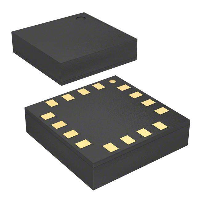
| 产品图片 |
|
| rohs | 符合RoHS无铅 / 符合限制有害物质指令(RoHS)规范要求 |
| 产品系列 | 螺旋仪,Maxim Integrated MAX21000+- |
| 数据手册 | |
| 产品型号 | MAX21000+ |
| 产品种类 | 螺旋仪 |
| 传感轴 | X, Y, Z |
| 供应商器件封装 | 16-LGA(3x3) |
| 典型带宽 | 400Hz |
| 加速 | 10000 g |
| 商标 | Maxim Integrated |
| 宽度 | 3 mm |
| 封装 | Tube |
| 封装/外壳 | 16-VFLGA |
| 封装/箱体 | LGA-16 |
| 工作温度 | -40°C ~ 85°C |
| 工厂包装数量 | 100 |
| 带宽 | 400 Hz |
| 应用说明 | |
| 数字输出-位数 | 16 bit |
| 数字输出-总线接口 | I2C, SPI |
| 最大工作温度 | + 85 C |
| 最小工作温度 | - 40 C |
| 标准包装 | 1 |
| 灵敏度 | 960 digit/dps |
| 特色产品 | http://www.digikey.cn/product-highlights/zh/ultraaccurate-lowpower-3axis-digital-output-gyroscope/51078 |
| 电压-电源 | 1.71 V ~ 3.6 V |
| 电流-电源 | 5.4mA |
| 电源电压-最大 | 3.6 V |
| 电源电压-最小 | 1.71 V |
| 电源电流 | 5.4 mA |
| 系列 | MAX21000 |
| 范围 | +/- 31.5 deg/s, +/- 62.5 deg/s, +/- 125 deg/s, +/- 250 deg/s, +/- 500 deg/s, +/- 1000 deg/s, +/- 2000 deg/s |
| 范围°/s | - |
| 输出类型 | Digital |
| 长度 | 3 mm |
| 零件号别名 | 90-N2100+000 |
| 高度 | 0.9 mm |


- 商务部:美国ITC正式对集成电路等产品启动337调查
- 曝三星4nm工艺存在良率问题 高通将骁龙8 Gen1或转产台积电
- 太阳诱电将投资9.5亿元在常州建新厂生产MLCC 预计2023年完工
- 英特尔发布欧洲新工厂建设计划 深化IDM 2.0 战略
- 台积电先进制程称霸业界 有大客户加持明年业绩稳了
- 达到5530亿美元!SIA预计今年全球半导体销售额将创下新高
- 英特尔拟将自动驾驶子公司Mobileye上市 估值或超500亿美元
- 三星加码芯片和SET,合并消费电子和移动部门,撤换高东真等 CEO
- 三星电子宣布重大人事变动 还合并消费电子和移动部门
- 海关总署:前11个月进口集成电路产品价值2.52万亿元 增长14.8%

PDF Datasheet 数据手册内容提取
EVALUATION KIT AVAILABLE MAX21000 Ultra-Accurate, Low Power, 3-Axis Digital Output Gyroscope General Description ● OIS Suitability • Minimum Phase Delay (~3º at 10Hz) The MAX21000 is a low power, low noise, 3-axis angular • High Bandwidth (400Hz) rate sensor that delivers unprecedented accuracy and • High ODR (10kHz) sensitivity over temperature and time. It operates with a supply voltage as low as 1.71V for minimum power • Low Noise (9mdps/√Hz typ) consumption. It includes a sensing element and an IC • Four Different FS in OIS Mode: ±31.25/±62.50/±125/±250 dps interface that provides the measured angular rate to the external world through a digital interface (I2C/SPI). ● Unprecedented Accuracy and Stability The IC has a full scale of ±31.25/±62.50/±125/±250/ • Embedded Digital-Output Temperature Sensor ±500/±1k/±2k degrees per second (dps) and measures • Automatic Temperature Compensation rates with a finely tunable user-selectable bandwidth. The • Ultra-Stable Over Temperature and Time high ODR and the large BW, the low noise at highest FS, • Factory Calibrated together with the low phase delay, make the IC suitable ● High-Speed Interface for both user interface (UI) and optical image stabilization • I2C Standard (100kHz), Fast (400kHz), and (OIS) applications. High-Speed (3.4MHz) Serial Interface The IC is a highly integrated solution available in a com- • 10MHz SPI Interface pact 3mm x 3mm x 0.9mm plastic land grid array (LGA) • Reduces AP Load package and does not require any external components • Enables UI/OIS Serial Interface Multiplexing other than supply bypass capacitors. It can operate over ● Flexible Embedded FIFO the -40ºC to +85ºC temperature range. • Size: 512bytes (256 x 16 bits) Applications • Single-Byte Reading Available • Four Different FIFO Modes Available ● Motion Control with MMI (Man-Machine Interface) • Reduces AP Load ● No Touch UI ● GPS Navigation Systems ● High Configurability ● Appliances and Robotics • Integrated Digitally Programmable Low- and ● Motion-Enabled Game Controllers Highpass Filters ● Motion-Based Portable Gaming • Independently Selectable Data ODR and Interrupt ● Motion-Based 3D Mouse and 3D Remote Controls ODR ● Health and Sports Monitoring • 7 Selectable Full Scales (31.25/62.5/125/250/500/ 1000/2000 dps) ● Optical Image Stabilization • 256 Selectable ODR Ordering Information appears at end of data sheet. ● Flexible Interrupt Generator For related parts and recommended products to use with this part, refer • Two Digital Output Lines to www.maximintegrated.com/MAX21000.related. • 2 Independent Interrupt Generators Benefits and Features • 8 Maskable Interrupt Sources Each • Configurable as Latched/Unlatched/Timed ● Minimum Overall Footprint • Embedded Independent Angular Rate Comparators • Industry’s Smallest and Thinnest Package for • Independent Threshold and Duration Portable Devices (3mm x 3mm x 0.9mm LGA) • Level/Pulse and OD/PP Options Available • No external components ● Unique Low-Power Capabilities ● Flexible Data Synchronization Pin • External Wakeup • Low Operating Current Consumption (5.4mA typ) • Interrupt Generation • Eco Mode Available at 100Hz with 3.0mA (typ) • Single Data Capture Trigger • 1.71V (min) Supply Voltage • Multiple Data Capture Trigger • Standby Mode Current 2.7mA (typ) • LSB Data Mapping • 9µA (typ) Power-Down Mode Current • High PSRR and DC-DC Converter Operation ● Unique 48-Bit Serial Number as Die ID • 45ms Turn-On Time from Power-Down Mode ● High-Shock Survivability (10,000 G-Shock) • 5ms Turn-On Time from Standby Mode 19-6567; Rev 1; 2/13
MAX21000 Ultra-Accurate, Low Power, 3-Axis Digital Output Gyroscope Absolute Maximum Ratings VDD .......................................................................-0.3V to +6.0V IVDDIO Continuous Current ..............................................100mA VDDIO .....................................-0.3V to Min (VDD + 0.3V, +6.0V) Junction Temperature ......................................................+150ºC INT1, INT2, SDA_SDI_O, SA0_SDO, Operating Temperature Range ............................-40ºC to +85ºC SCL_CLK, CS, DSYNC .....................-0.3V to (VDDIO + 0.3V) Storage Temperature Range .............................-40ºC to +150ºC IVDD Continuous Current .................................................100mA Lead Temperature (soldering, 10s) .................................+260ºC Stresses beyond those listed under “Absolute Maximum Ratings” may cause permanent damage to the device. These are stress ratings only, and functional operation of the device at these or any other conditions beyond those indicated in the operational sections of the specifications is not implied. Exposure to absolute maximum rating conditions for extended periods may affect device reliability. Drops onto hard surfaces can cause shocks of greater than 10,000 g and can exceed the absolute maximum rating of the device. Exercise care in handling to avoid damage. Package Thermal Characteristics(Note 1) LGA Junction-to-Case Thermal Resistance (θJC) ...........31.8°C/W Junction-to-Ambient Thermal Resistance (θJA) ...........160°C/W Note 1: Package thermal resistances were obtained using the method described in JEDEC specification JESD51-7, using a four-layer board. For detailed information on package thermal considerations, refer to www.maximintegrated.com/thermal-tutorial. Electrical Characteristics (VDD = VDDIO = 2.5V, INT1, INT2, TA = -40°C to +85°C, SDA and SCL are unconnected, unless otherwise noted. Typical values are at TA = +25°C). PARAMETER SYMBOL CONDITIONS MIN TYP MAX UNITS SUPPLY AND CONSUMPTION VDD Supply Voltage VDD 1.71 2.5 3.6 V VDDIO (Note 2) VDDIO 1.71 2.5 V0D.3DV + V IDD Current Consumption Normal Mode IVDDN 5.4 mA IDD Current Consumption Standby Mode (Note 3) IVDDS 2.7 mA IDD Current Consumption 200Hz ODR 3.3 mA Eco Mode (Note 4) IVDDT 100Hz ODR 3.0 mA IDD Current Consumption Power Down Mode IVDDP 8.5 µA TEMPERATURE SENSOR Temperature Sensor Output 8 bit 1 digit/ºC Change vs. Temperature TSDR 16 bit 256 digit/ºC Temperature BW TBW 1 Hz At TA = +25ºC, 8 bit 25 Temperature Sensor Bias TBIAS digit At TA = +25ºC, 16 bit 6400 GYROSCOPE ±31.25 ±62.5 Gyro Full-Scale Range GFSR User selectable dps ±125 ±250 www.maximintegrated.com Maxim Integrated │ 2
MAX21000 Ultra-Accurate, Low Power, 3-Axis Digital Output Gyroscope Electrical Characteristics (continued) (VDD = VDDIO = 2.5V, INT1, INT2, TA = -40°C to +85°C, SDA and SCL are unconnected, unless otherwise noted. Typical values are at TA = +25°C). PARAMETER SYMBOL CONDITIONS MIN TYP MAX UNITS ±500 Gyro Full-Scale Range GFSR User selectable ±1000 dps ±2000 Gyro Rate Noise Density GRND iFnocrlu adlli nthge 1 f.S8 Va nd over the whole VDD 0.009 dps/√Hz GEcyoro M Roadtee Noise Density in GSPRND Finocrl uadlli nthge 1 F.8SV a antd 2 o0v0eHrz t hOeD wRhole VDD 0.025 dps/√Hz Gyro Bandwidth (Lowpass) (Note 5) GBWL 2 400 Hz Gyro Bandwidth (Highpass) (Note 6) GBWH 0.1 100 Hz Phase Delay GPDL At 10Hz, 400Hz bandwidth, 10kHz ODR 2.9 deg Output Data Rate (Note 7) GODR 5 10k Hz Sensitivity Error GSE ±2 % GFSR = 31.25 960 GFSR = 62.5 480 GFSR = 125 240 digit/ Sensitivity GSO GFSR = 250 120 dps GFSR = 500 60 GFSR = 1000 30 GFSR = 2000 15 Sensitivity Drift Over Temperature GSD Maximum delta from TA = +25ºC ±2 % Zero Rate Level Error GZRLE ±0.5 dps Zero Rate Level Drift Over Temperature GZRLD Maximum delta from TA = +25ºC ±2 dps Startup Time from Power Down GTUPL 45 ms Startup Time from Standby Mode GTUPS GGOBWDRL == 41000kHHzz, 2 ms Nonlinearity GNLN 0.2 %fS Angular Random Walk (ARW) GARW 0.45 º/√hr In-Run Bias Stability GIBS At 1000s 4 º/hr Cross Axis GXX 1 % For GFSR = 250, 500, 1000, 2000 dps, axes X, Z +fS/4 Self-Test Output STOR dps For GFSR = 250, 500, 1000, 2000 dps, axis Y -fS/4 www.maximintegrated.com Maxim Integrated │ 3
MAX21000 Ultra-Accurate, Low Power, 3-Axis Digital Output Gyroscope Electrical Characteristics (continued) (VDD = VDDIO = 2.5V, INT1, INT2, TA = -40°C to +85°C, unless otherwise noted. Typical values are at TA = +25°C). PARAMETER SYMBOL CONDITIONS MIN TYP MAX UNITS IO DC SPECIFICATIONS (Note 9) +0.3 x Input Threshold Low VIL TA = +25ºC VDDIO V 0.7 x Input Threshold High VIH TA = +25ºC VDDIO V 0.05 x Hysteresis of Schmitt Trigger input VHYS TA = +25ºC VDDIO V I2C_CFG[3:2] = 00 3 mA Output Current (Note 8) IOH/IOL I2C_CFG[3:2] = 01 6 mA I2C_CFG[3:2] = 11 12 mA SPI SLAVE TIMING VALUES (Note 10) CLK Frequency FC_CLK 10 MHz CS Setup Time tSU_CS 6 ns CS Hold Time tH_CS 12 ns SDI Input Setup Time tSU_SI 6 ns SDI Input Hold Time tH_SI 12 ns CLK Fall to SDO Valid Output Time tV_SDO 50 ns SDO Output Hold Time TH_SO 10 ns ESD PROTECTION Human Body Model HBM ±2 kV Note 2: VDDIO must be lower or equal than VDD analog. Note 3: In standby mode, only the drive circuit is powered on. In this condition, the outputs are not available. In this condition, the startup time depends only on the filters responses. Note 4: In eco mode, the sensor has higher rate noise density, but lower current consumption. In this condition, the selectable out- put data rate (ODR) is either 25Hz, 50Hz, 100Hz, or 200Hz. Note 5: User selectable: gyro bandwidth accuracy is ±10%. Note 6: Enable/disable with user selectable bandwidth. Gyro bandwidth accuracy is ±10%. Note 7: User selectable with 256 possible values from 10kHz down to 5Hz. ODR accuracy is ±10%. Note 8: User can choose the best output current based on his PCB, interface speed, load, and consumption. Note 9: Based on characterization results, not production tested. Note 10:Based on characterization results, not production tested. Test conditions are: I2C_CFG[3:0] = 1111. www.maximintegrated.com Maxim Integrated │ 4
MAX21000 Ultra-Accurate, Low Power, 3-Axis Digital Output Gyroscope SPI Timing Diagrams 4-WIRE SPI MODE tCSW tSU_CS CS tH_CS CLK 1 2 8 9 10 tC_CLK tSU_SI SDI tH_SI tH_SO tV_SDO HI-Z HI-Z SDO 3-WIRE SPI MODE tCSW tSU_CS CS tH_CS CLK 1 2 8 9 10 tC_CLK tSU_SI HI-Z SDI tH_SI HI-Z SDO www.maximintegrated.com Maxim Integrated │ 5
MAX21000 Ultra-Accurate, Low Power, 3-Axis Digital Output Gyroscope Typical Operating Characteristics (VDD = VDDIO = 2.5V, TA = +25ºC, unless otherwise noted.) X-AXIS DIGITAL OUTPUT Y-AXIS DIGITAL OUTPUT Z-AXIS DIGITAL OUTPUT vs. ANGULAR RATE vs. ANGULAR RATE vs. ANGULAR RATE b) 2300kk MAX21000 toc01 b) 2300kk MAX21000 toc02 b) 2300kk TA = -40°C MAX21000 toc03 S S S T (L 10k T (L 10k T (L 10k U U U P P P T T T OU 0 TA = +25°C OU 0 TA = +25°C OU 0 L L L A A A T T T GI-10k TA = -40°C GI-10k TA = -40°C GI-10k DI DI DI TA = +85°C TA = +85°C TA = +85°C -20k -20k -20k TA = +25°C -30k -30k -30k -2k -1k 0 1k 2k -2k -1k 0 1k 2k -2k -1k 0 1k 2k ANGULAR RATE (dps) ANGULAR RATE (dps) ANGULAR RATE (dps) ZERO-RATE LEVEL vs. POWER SUPPLY MAGNITUDE RESPONSE PHASE RESPONSE 001...680 MAX21000 toc04 100 BW = 400Hz MAX21000 toc05 --21000 MAX21000 toc06 ZERO-RATE (dps) -000...2240 Y X MAGNITUDE (dB) ---321000 BW = 10Hz BW = 100Hz PHASE (deg) ----65430000 BW =B 1W0H =z 100BHWz = 400Hz -0.4 Z -0.6 -70 -40 -0.8 -80 -1.0 -50 -90 1.6 2.1 2.6 3.1 3.6 1 10 100 1000 0 100 200 300 400 500 POWER SUPPLY (V) FREQUENCY (Hz) FREQUENCY (Hz) www.maximintegrated.com Maxim Integrated │ 6
MAX21000 Ultra-Accurate, Low Power, 3-Axis Digital Output Gyroscope Pin Configuration TOP VIEW N.C. VDD VDD + 16 15 14 VDDIO 1 13 RESERVED N.C. 2 12 DSYNC MAX21000 N.C. 3 11 INT1 SCL_CLK 4 10 RESERVED GND 5 9 INT2 6 7 8 O O S _ D C DI S DA_S SA0_ S LGA (3mm x 3mm) Pin Description PIN NAME FUNCTION 1 VDD_IO Interface and Interrupt Pad Supply Voltage 2, 3, 16 N.C. Not Internally Connected SPI and I2C Clock. When in I2C mode, the IO has selectable antispike filter and delay to ensure 4 SCL_CLK correct hold time. 5 GND Power-Supply Ground. SPI In/Out Pin and I2C Serial Data. When in I2C mode, the IO has selectable antispike filter and 6 SDA_SDI_O delay to ensure correct hold time. 7 SA0_SDO SPI Serial Data Out or I2C Slave Address LSB 8 CS SPI Chip Select/Serial Interface Selection 9 INT2 Second Interrupt Line 10 RESERVED Must Be Connected to GND 11 INT1 First Interrupt Line Data Synchronization Pin. Used to wake up the MAX21000 from power down/standby and 12 DSYNC synchronize data with GPS/camera. 13 RESERVED Leave Unconnected 14 VDD Analog Power Supply. Bypass to GND with a 0.1µF capacitor and one 1µF. 15 VDD Must be tied to VDD in the application. www.maximintegrated.com Maxim Integrated │ 7
MAX21000 Ultra-Accurate, Low Power, 3-Axis Digital Output Gyroscope Functional Diagram TIMER MEMS MAX21000 GYRO SENSE SCL_CLK FILTERING SDA_SDI_O A AFE SPI/I2C SA0_SDO SLAVE REGISTERS CS AND A AFE FIFO GYRO DSYNC SYNC DRIVE CONTROL A AFE INT1 INTERRUPTS INT2 RING OSCILLATOR GND VDD VDD_IO Detailed Description power the MEMS gyroscope, the MAX21000 can not only operate at 1.71V but that supply can also be provided by The MAX21000 is a low power, low voltage, small a switching regular, to minimize the system power con- package three-axis angular rate sensor able to provide sumption. unprecedented accuracy and sensitivity over temperature and time. Power-supply current (mA): This parameter defines the typical current consumption when the MEMS gyroscope The IC is also the industry’s first gyroscope available in a is operating in normal mode. 3mm x 3mm package and capable of working with a sup- ply voltage as low as 1.71V. Power-supply current in standby mode (mA): This parameter defines the current consumption when the It includes a sensing element and an IC interface that MEMS gyroscope is in Standby mode. To reduce power provides the measured angular rate to the external world consumption and have a faster turn-on time, in Standby through a digital interface (I2C/SPI). mode only an appropriate subset of the sensor is turned off. The IC has a full scale of ±250/±500/±1k/±2k dps for UI Power-supply current in eco mode (mA): This param- and ±31.25/±62.5/±125/±250 dps for OIS. It measures eter defines the current consumption when the MEMS rates with a user-selectable bandwidth. gyroscope is in a special mode named eco mode. While The IC is available in a 3mm x 3mm x 0.9 mm plastic land in eco mode, the MAX21000 reduces significantly the grid array (LGA) package and operates over the -40ºC to power consumption, at the price of a slightly higher rate +85ºC temperature range. noise density. See the Definitions section for more information. Power-supply current in power-down mode (µA): This parameter defines the current consumption when Definitions the MEMS gyroscope is powered down. In this mode, Power supply (V): This parameter defines the operating both the mechanical sensing structure and reading chain DC power-supply voltage range of the MEMS gyroscope. are turned off. Users can configure the control register Although it is always a good practice to keep VDD clean through the I2C/SPI interface for this mode. Full access with minimum ripple, unlike most of the competitors, to the control registers through the I2C/SPI interface is who require an ultra-low noise, low-dropout regulator to guaranteed also in power-down mode. www.maximintegrated.com Maxim Integrated │ 8
MAX21000 Ultra-Accurate, Low Power, 3-Axis Digital Output Gyroscope Full-scale range (dps): This parameter defines the mea- Three-Axis MEMS Gyroscope with 16-Bit ADCs surement range of the gyroscope in degrees per second and Signal Conditioning (dps). When the applied angular velocity is beyond the The IC consists of a single-drive vibratory MEMS gyro- full-scale range, the gyroscope output signal is saturated. scope that detects rotations around the X, Y, and Z axes. Zero-rate level (dps): This parameter defines the zero- When the gyroscope rotates around any of the sensing rate level when there is no angular velocity applied to the axes, the Coriolis Force determines a displacement, which can be detected as a capacitive variation. The resulting gyroscope. signal is then processed to produce a digital stream pro- Sensitivity (digit/dps): Sensitivity (digit/dps) is the rela- portional to the angular rate. The analog-to-digital con- tionship between 1 LSB and dps. It can be used to version uses 16-bit ADC converters. The gyro full-scale convert a digital gyroscope’s measurement in LSBs to range can be digitally programmed to ±250, ±500, ±1000 angular velocity. or ±2000 dps in UI mode and ±31.25/±62.5/±125/±250 Sensitivity change vs. temperature (%): This parameter dps in OIS mode. defines the sensitivity change in percentage (%) over the Interrupt Generators operating temperature range specified in the data sheet. The MAX21000 offers two completely independent inter- Zero-rate level change vs. temperature (dps): This rupt generators to ease the SW management of the inter- parameter defines the zero-rate level change in dps over rupt generated. For instance, one line could be used to the operating temperature range. signal a DATA_READY event whilst the other line might Non-linearity (% FS): This parameter defines the maxi- be used, for instance, to notify the completion of the inter- mum error between the gyroscope‘s outputs and the best- nal startup sequence. fit straight line in percentage with respect to the full-scale Interrupt functionality can be configured through the (FS) range. Interrupt Configuration registers. Configurable items System bandwidth (Hz): This parameter defines the include the INT pin level and duration, the clearing frequency of the angular velocity signal from DC to the method, as well as the required triggers for the interrupts. built-in bandwidth (BW) that the gyroscopes can measure. The interrupt status can be read from the Interrupt Status A dedicated register can be modified to adjust the gyro- Registers. The event that has generated an interrupt is scope’s bandwidth. available in two forms: latched and unlatched. Rate noise density (dps/√Hz): This parameter defines Interrupt sources can be enabled/disabled and cleared indi- the standard resolution that users can get from the gyro- vidually. The list of possible interrupt sources includes the scopes outputs together with the BW parameter. following conditions: DATA_READY, FIFO_READY, FIFO_ THRESHOLD, FIFO_OVERRUN, RESTART, DSYNC. MAX21000 Architecture The interrupt generation can also be configured as The MAX21000 comprises the following key blocks and latched, unlatched, or timed with programmable length. functions: When configured as latched, the interrupt can be cleared ● Three-axis MEMS rate gyroscope sensor with 16-bit by reading the corresponding status register (clear-on- ADCs and signal conditioning read) or by writing an appropriate mask to the status ● Primary I2C and SPI serial communications interfaces register (clear-on-write). ● Sensor data registers Digital-Output Temperature Sensor ● FIFO A digital output temperature sensor is used to measure ● Synchronization the IC die temperature. The readings from the ADC can be accessed from the Sensor Data registers. ● Interrupt generators ● Digital output temperature sensor The temperature data is split over 2 bytes. For faster and less accurate reading, accessing the MSB allows to read ● Self-test the temperature data as an absolute value expressed in Celsius degrees (ºC). By reading the LSB, the accuracy is greatly increased, up to 256 digit/ºC. www.maximintegrated.com Maxim Integrated │ 9
MAX21000 Ultra-Accurate, Low Power, 3-Axis Digital Output Gyroscope Power Modes Table 1. Power Modes The IC features four power modes, allowing selecting the NAME DESCRIPTION appropriate tradeoff between power consumption, accu- racy, and turn-on time. Device is operational with maximum Normal performances. The transition between power modes can be controlled by software, by explicitly setting a power mode in the Eco Device operates to reduce the average current consumption. Configuration register, or by enabling the automatic power mode transition based on the DSYNC pin. In standby mode, the current consumption is Standby reduced by 50%, with a shorter turn-on time Normal Mode of 5ms. In normal mode, the IC is operational with minimum noise This is the minimum power consumption level. Power-Down mode, at the price of a longer turn-on time. Eco Mode The eco mode reduces power consumption with the same Table 2. Digital Interface Pin Description sensor accuracy at the price of a higher rate noise density. This unique feature can be activated with four ODRs: NAME DESCRIPTION 25Hz, 50Hz, 100Hz, and 200Hz. SPI enable and I2C/SPI mode selection CS (1: I2C mode, 0: SPI enabled) Standby Mode To reduce power consumption and have a shorter turn-on SPI and I2C clock. When in I2C mode, the IO time, the IC features a standby mode. In standby mode, SCL/CLK has selectable anti-spike filter and delay to the IC does not generate data, as a significant portion of ensure correct hold time. the signal processing resources is turned off to save power. SPI in/out pin and I2C serial data. When in SDA/SDI/ Still, this mode enables a much quicker turn-on time. I2C mode, the IO has selectable anti-spike SDO filter and delay to ensure correct hold time. Power-Down Mode In power-down mode, the IC is configured to minimize the SDO/SA0 SPI serial data out or I2C slave address LSB power consumption. In power-down mode, registers can still be read and written, but the gyroscope cannot generate new Table 3. I2C Address data. Compared to the standby mode, it takes longer to acti- I2C BASE SA0/SDO RESULTING vate the IC and to start collecting data from the gyroscope. R/W BIT ADDRESS PIN ADDRESS Digital Interfaces 0x2C (6 bit) 0 0 0xB0 The registers embedded inside the IC can be accessed 0x2C 0 1 0xB1 through both the I2C and SPI serial interfaces. The latter 0x2C 1 0 0xB2 can be SW-configured to operate either in 3-wire or 4-wire interface mode. 0x2C 1 1 0xB3 The serial interfaces are mapped onto the same pins. To select/exploit the I2C interface, CS line must be tied high The IC always operates as a slave device when commu- nicating to the system processor, which thus acts as the (i.e., connected to VDDIO). master. SDA and SCL lines typically need pullup resistors I2C Interface to VDDIO. The maximum bus speed is 3.4MHz (I2C HS); I2C is a two-wire interface comprised of the signals this reduces the amount of time the system processor is serial data (SDA) and serial clock (SCL). In general, the kept busy in supporting the exchange of data. lines are open-drain and bidirectional. In a generalized The slave address of the IC is b101100X, which is 7 bits I2C interface implementation, attached devices can be long. The LSb of the 7-bit address is determined by the a master or a slave. The master device puts the slave logic level on pin SA0. This allows two MAX21000s to be address on the bus, and the slave device with the match- connected on the same I2C bus. When used in this con- ing address acknowledges the master. figuration, the address of one of the two devices should www.maximintegrated.com Maxim Integrated │ 10
MAX21000 Ultra-Accurate, Low Power, 3-Axis Digital Output Gyroscope be b1011000 (pin SA0_SD0 is set to logic-low) and the Full-Duplex Operation address of the other should be b1011001 (pin SA0_SD0 The IC is put into full-duplex mode at power-up, or when is set to logic-high). the SPI master clears the SPI_3_WIRE bit, the SPI inter- face uses separate data pins, SDI and SDO to transfer SPI Interface data. Because of the separate data pins, bits can be The IC’s SPI can operate up to 10MHz, in both 3-wires simultaneously clocked into and out of the IC. The IC (half duplex) and 4-wires mode (full duplex). makes use of this feature by clocking out 8 output data It is recommended to set the I2C_DISABLE bit at address bits as the command byte is clocked in. 0x15 if the IC is used together with other SPI devices to avoid the possibility to switch inadvertently into I2C mode Reading from the SPI Slave Interface (SDO) when traffic is detected with the CS unasserted. The SPI master reads data from the IC slave interface using the following steps: The IC operates as an SPI slave device. Both the read register and write register commands are completed in 16 1) When CS is high, the IC is unselected and three-states clock pulses, or in multiples of 8 in case of multiple read/ the SDO output. write bytes. Bit duration is the time between two falling 2) After driving SCL_CLK to its inactive state, the SPI edges of CLK. master selects the IC by driving CS low. The first bit (bit 0) starts at the first falling edge of CLK 3) The SPI master simultaneously clocks the command after the falling edge of CS while the last bit (bit 15, bit 23, byte into the MAX21000. The SPI Read command etc.) starts at the last falling edge of CLK just before the is performed with 16 clock pulses. Multiple byte read rising edge of CS. command is performed adding blocks of 8 clock pulses Bit 0: RW bit. When 0, the data DI[7:0] is written to the at the previous one. IC. When 1, the data DO[7:0] from the device is read. In Bit 0: READ bit. The value is 1. the latter case, the chip drives SDO at the start of bit 8. Bit 1: MS bit. When 1, do not increment address. Bit 1: MS bit. Depending on the configuration of When 0, increment address in multiple reading. IF_PARITY, this bit can either be used to operate in Bits 2–7: address AD[5:0]. This is the address field of multi-addressing standard mode or to check the parity the indexed register. with the register address. Bits 8–15: data DO[7:0] (read mode). This is the data If used as MS bit, when 1, the address remains that is read from the device (MSb first). unchanged in multiple read/write commands. When 0, the address is autoincremented in multiple read/write Bits 16–... : data DO[...–8]. Further data in multiple commands. byte reading. Bits 2–7: Address AD[5:0]. This is the address field of 4) After 16 clock cycles, the master can drive CS high to the indexed register. deselect the IC, causing it to three-state its SDO out- put. The falling edge of the clock puts the MSB of the Bits 8–15: Data DI[7:0] (write mode). This is the data next data byte in the sequence on the SDO output. that is written to the device (MSb first). 5) By keeping CS low, the master clocks register data Bits 8–15: Data DO[7:0] (read mode). This is the data bytes out of the IC by continuing to supply SCL_CLK that is read from the device (MSb first). pulses (burst mode). The master terminates the trans- SPI Half- and Full-Duplex Operation fer by driving CS high. The master must ensure that The IC can be programmed to operate in half-duplex (a SCL_CLK is in its inactive state at the beginning of the bidirectional data pin) or full-duplex (one data-in and one next access (when it drives CS low). data-out pin) mode. The SPI master sets a register bit called SPI_3_WIRE into ITF_OTP to 0 for full-duplex, and 1 for half-duplex operation. Full duplex is the power-on default. www.maximintegrated.com Maxim Integrated │ 11
MAX21000 Ultra-Accurate, Low Power, 3-Axis Digital Output Gyroscope Writing to the SPI Slave Interface (SDI) Bit 0: READ bit. The value is 1. The SPI master writes data to the IC slave interface Bit 1: MS bit. When 1, do not increment address. through the following steps: When 0, increment address in multiple readings. 1) The SPI master sets the clock to its inactive state. Bit 2–7: Address AD[5:0]. This is the address field of When CS is high, the master can drive the SDI input. the indexed register. 2) The SPI master selects the MAX21000 by driving CS low. Bit 8–15: data DO[7:0] (read mode). This is the data that is read from the device (MSb first). Multiple read 3) The SPI master simultaneously clocks the command command is also available in 3-wire mode. byte into the IC. The SPI write command is performed with 16 clock pulses. Multiple byte write command is Sensor Data Registers performed adding blocks of 8 clock pulses at the previ- The sensor data registers contain the latest gyroscope ous one. and temperature measurement data. Bit 0: WRITE bit. The value is 0. They are read-only registers and are accessed through Bit 1: MS bit. When 1, do not increment address, the serial interface. Data from these registers can be read when 0, increment address in multiple writing. anytime. However, the interrupt function can be used to Bits 2–7: address AD[5:0]. This is the address field of determine when new data is available. the indexed register. FIFO Bits 8–15: data DI[7:0] (write mode). This is the data The IC embeds a 256-slot of a 16-bit data FIFO for each that is written inside the device (MSb first). of the three output channels: yaw, pitch, and roll. This Bits 16–... : data DI[...–8]. Further data in multiple byte allows a consistent power saving for the system since the writing. host processor does not need to continuously poll data 4) By keeping CS low, the master clocks data bytes into from the sensor, but it can wake up only when needed the IC by continuing to supply SCL_CLK pulses (burst and burst the significant data out from the FIFO. When mode). The master terminates the transfer by driving configured in Snapshot mode, it offers the ideal mecha- CS high. The master must ensure that SCL_CLK is nism to capture the data following a Rate Interrupt event. inactive at the beginning of the next access (when it This buffer can work according to four main modes: off, drives CS low). In full-duplex mode, the IC outputs normal, interrupt, and snapshot. data bits on SDO during the first 8 bits (the command Both Normal and Interrupt modes can be optionally byte), and subsequently outputs zeros on SDO as the configured to operate in overrun mode, depending on SPI master clocks bytes into SDI. whether, in case of buffer under-run, newer or older data Half-Duplex Operation are lost. When the SPI master sets SPI_3_WIRE = 1, the IC is put Various FIFO status flags can be enabled to generate into half-duplex mode. In half-duplex mode, the IC three- interrupt events on INT1/INT2 pin. states its SDO pin and makes the SDI pin bidirectional, FIFO Off Mode saving a pin in the SPI interface. The SDO pin can be left In this mode, the FIFO is turned off; data are stored only unconnected in half-duplex operation. The SPI master in the data registers and no data are available from the must operate the SDI pin as bidirectional. It accesses a FIFO if read. IC register as follows: the SPI master sets the clock to its inactive state. While CS is high, the master can drive the When the FIFO is turned off, there are essentially two SDI pin to any value. options to use the device: synchronous and asynchro- nous reading. 1) The SPI master selects the IC by driving CS low and placing the first data bit (MSB) to write on the SDI Synchronous Reading input. In this mode, the processor reads the data set (e.g., 6 2) The SPI master turns on its output driver and clocks the bytes for a 3 axes configuration) generated by the IC command byte into the IC. The SPI read command is every time that DATA_READY is set. The processor must performed with 16 clock pulses: read once and only once the data set in order to avoid data inconsistencies. www.maximintegrated.com Maxim Integrated │ 12
MAX21000 Ultra-Accurate, Low Power, 3-Axis Digital Output Gyroscope Benefits of using this approach include the perfect recon- data rate (ODR). struction of the signal coming the gyroscope and mini- ● When FIFO is full, an interrupt can be generated. mum data traffic. ● When FIFO is full, all the new incoming data is dis- Asynchronous Reading charged. Reading only a subset of the data already In this mode, the processor reads the data generated by stored into the FIFO keeps locked the possibility the IC regardless the status of the DATA_READY flag. To for new data to be written. minimize the error caused by different samples being read ● Only if all the data are read, the FIFO restarts sav- a different number of times, the access frequency to be ing data. used must be much higher than the selected ODR (e.g., ● If communication speed is high, data loss can be 10x). This approach normally requires a much higher BW. prevented. FIFO Normal Mode ● To prevent a FIFO-FULL condition, the required Overrun = false condition is to complete the reading of the data set ● FIFO is turned on. before the next DATA_READY occurs. ● FIFO is filled with the data at the selected output ● If this condition is not guaranteed, data can be lost. 255 255 255 (WP-RP) = LEVEL (WP-RP) = LEVEL (WP-RP) = THRESHOLD THRESHOLD THRESHOLD LEVEL 0 0 0 LEVEL INCREMENTS WITH NEW FIFO_FULL INTERRUPT GENERATED. FIFO_OVTHOLD INTERRUPT SAMPLES STORED AND DECREMENTS NO NEW DATA STORED UNTIL GENERATED. WITH NEW READINGS. THE ENTIRE FIFO IS READ. Figure 1. FIFO Normal Mode, Overrun = False www.maximintegrated.com Maxim Integrated │ 13
MAX21000 Ultra-Accurate, Low Power, 3-Axis Digital Output Gyroscope Overrun = true Interrupt Mode ● FIFO is turned on. Overrun = false ● FIFO is filled with the data at the selected ODR. ● FIFO is initially disabled. Data are stored only in the data registers. ● When FIFO is full, an interrupt can be generated. ● When a rate interrupt (either OR or AND) is gener- ● When FIFO is full, the oldest data is overwritten- ated, the FIFO is turned on automatically. It stores with the new ones. the data at the selected ODR. ● If communication speed is high, data integrity can ● When FIFO is full, all the new incoming data is dis- be preserved. charged. Reading only a subset of the data already ● To prevent a DATA_LOST condition, the required stored into the FIFO keeps locked the possibility condition is to complete the reading of the data set for new data to be written. before the next DATA_READY occurs. ● Only if all the data are read, the FIFO restarts sav- ● If this condition is not guaranteed, data can be ing data. overwritten. ● If communication speed is high, data loss can be ● When an overrun condition occurs the reading prevented. pointer is forced to writing pointer -1 to ensure only ● To prevent a FIFO-FULL condition, the required older data are discarded and newer data have a condition is to complete the reading of the data set chance to be read. before the next DATA_READY occurs. ● If this condition is not guaranteed, data can be lost. FIFO USED AS FIFO USED AS FIFO USED AS CIRCULAR BUFFER CIRCULAR BUFFER CIRCULAR BUFFER RP WP WP THRESHOLD THRESHOLD THRESHOLD RP WP RP WP-RP INCREMENTS WITH NEW FIFO_FULL INTERRUPT GENERATED. FIFO_OVTHOLD INTERRUPT SAMPLES STORED AND DECREMENTS NEW INCOMING DATA WOULD GENERATED. WITH NEW READINGS. OVERWRITE THE OLDER ONES. Figure 2. FIFO Normal Mode, Overrun = True www.maximintegrated.com Maxim Integrated │ 14
MAX21000 Ultra-Accurate, Low Power, 3-Axis Digital Output Gyroscope MAX FIFO INITIALLY OFF. WHEN THE PROGRAMMED RATE INTERRUPT OCCURS, TURN FIFO ON. LEVEL 0 MAX MAX MAX (WP-RP) = LEVEL (WP-RP) = LEVEL (WP-RP) THRESHOLD THRESHOLD THRESHOLD = LEVEL 0 0 0 LEVEL INCREMENTS WITH NEW FIFO_FULL INTERRUPT GENERATED. FIFO_OVTHOLD INTERRUPT SAMPLES STORED AND DECREMENTS NO NEW DATA STORED UNTIL THE GENERATED. WITH NEW READINGS. ENTIRE FIFO IS READ. Figure 3. FIFO Interrupt Mode, Overrun = False www.maximintegrated.com Maxim Integrated │ 15
MAX21000 Ultra-Accurate, Low Power, 3-Axis Digital Output Gyroscope Overrun = true ● In order to prevent a DATA_LOST condition, the required condition is to complete the reading of the ● FIFO is initially disabled. Data are stored only in data set before the next DATA_READY occurs. the data registers. ● When a Rate Interrupt (either OR or AND) is ● If this condition is not guaranteed, data can be overwritten. generated, the FIFO is turned on automatically. It stores the data at the selected ODR. ● When an overrun condition occurs, the reading pointer is forced to writing pointer -1 to ensure only ● When FIFO is full, an interrupt can be generated. older data are discarded and newer data have a ● When FIFO is full, the oldest data is overwritten chance to be read. with the new ones. ● If communication speed is high, data integrity can be preserved. MAX FIFO INITIALLY OFF. WHEN THE PROGRAMMED RATE INTERRUPT OCCURS, TURN FIFO ON. LEVEL 0 RP WP WP THRESHOLD THRESHOLD THRESHOLD RP WP = RP WP-RP INCREMENTS WITH NEW FIFO_FULL INTERRUPT GENERATED. FIFO_OVTHOLD INTERRUPT SAMPLES STORED AND DECREMENTS NEW INCOMING DATA WOULD GENERATED. WITH NEW READINGS. OVERWRITE THE OLDER ONES. Figure 4. FIFO Interrupt Mode, Overrun = True www.maximintegrated.com Maxim Integrated │ 16
MAX21000 Ultra-Accurate, Low Power, 3-Axis Digital Output Gyroscope Snapshot Mode stored into the FIFO keeps locked the possibility for new data to be written. ● FIFO is initially in normal mode with overrun enabled. ● Only if all the data are read the FIFO restarts sav- ing data. ● When a Rate Interrupt (either OR or AND) is gen- erated, the FIFO switches automatically to not- ● If communication speed is high, data loss can be overrun mode. It stores the data at the selected prevented. ODR until the FIFO becomes full. ● To prevent a FIFO_FULL condition, the required ● When FIFO is full, an interrupt can be generated. condition is to complete the reading of the data set before the next DATA_READY occurs. ● When FIFO is full, all the new incoming data is dis- charged. Reading only a subset of the data already ● If this condition is not guaranteed, data can be lost. FIFO USED AS FIFO USED AS FIFO USED AS CIRCULAR BUFFER CIRCULAR BUFFER CIRCULAR BUFFER RP WP WP THRESHOLD THRESHOLD THRESHOLD RP WP RP RATE INTERRUPT SNAPSHOT CAPTURED MAX MAX MAX (WP-RP) = LEVEL (WP-RP) = LEVEL (WP-RP) THRESHOLD THRESHOLD THRESHOLD = LEVEL 0 0 0 Figure 5. FIFO Snapshot Mode www.maximintegrated.com Maxim Integrated │ 17
MAX21000 Ultra-Accurate, Low Power, 3-Axis Digital Output Gyroscope Bias Instability and Angular Random Walk DSYNC Interrupt Generation Bias instability is a critical performance parameter for The DSYNC pin can also be used as an interrupt source gyroscopes. The IC provides a typical bias instability of 4º/ to determine a different kind of data synchronization hour on each axis and an ARW of 0.45º/√hour, measured based on the software management performed by an using the Allan Variance method. external processor. The DSYNC-based wake-up, data capture, data map- Data Synchronization ping, and interrupt generation features can be combined The DSYNC pin enables a number of synchronization together. options. Unique Serial Number Wake-Up Feature Each IC is uniquely identified by 48 bits that can be used The DSYNC pin can be used to wake-up the IC from the to track the history of the sample, including manufactur- power-down or suspend mode. Repeatedly changing ing, assembly, and testing information. DSYNC from active to not active and vice-versa can be used to control the power mode of the MAX21000 using Self-Test an external controlling device, be it a microprocessor, For digital gyroscopes, there are two dedicated bits in a another sensor or a different kind of device. control register to enable the self-test. This feature can be DSYNC can be configured to active either High or Low used to verify if the gyroscope is working properly with- and on either edge or level. This feature is controlled by a out physically rotating the gyroscope. That may be used specific bit in the DSYNC_CFG register. either before or after it is assembled on a PCB. If the gyro- scope’s outputs are within the specified self-test values in Data Capture Feature the data sheet, then the gyroscope is working properly. Another way to use the DSYNC pin is as data capture trig- Therefore, the self-test feature is an important consider- ger. The IC can be configured to stop generating data until ation in a user’s end-product mass production line. a given edge occur on DSYNC. Once the programmed The embedded self-test in Maxim’s 3-axis digital gyro- active edge occurs, the IC collects as many data as speci- scope is an additional key feature that allows the gyro- fied in the DSYNC_CNT register. scope to be tested during final product assembly without DSYNC Mapping on Data requiring physical device movement. DSYNC can also be optionally mapped onto the LSB of the sensor data to perform synchronization afterwards. The mapping occurs on every enabled axis of the gyro- scope. This feature is controlled by a specific bit in the DSYNC_CFG register. www.maximintegrated.com Maxim Integrated │ 18
MAX21000 Ultra-Accurate, Low Power, 3-Axis Digital Output Gyroscope Register File addresses in the 0x00 to 0x3F range even though the number of physical registers is in excess of 64. The register file is organized per banks. On the common bank are mapped addresses from 0x20 to 0x3F and Common Bank these registers are always available. It is possible to map The common is the bank whose locations are always on addresses 0x00 to 0x1F two different user banks by available regardless the register bank selection. properly programming address 0x21. The purpose of this This bank contains all the registers most commonly used, structure is to limit the management of the register map including data registers and the FIFO data. Table 4. Common Bank REGISTER NAME TYPE DEFAULT VALUE COMMENT ADDRESS WHO_AM_I 0x20 R 1011 0001 Device ID BANK_SELECT 0x21 RW 0000 0000 Register bank selection SYSTEM_STATUS 0x22 R 0000 0000 System Status register GYRO_X_H 0x23 R Data Bits [15:8] of X measurement GYRO_X_L 0x24 R Data Bits [07:0] of X measurement GYRO_Y_H 0x25 R Data Bits [15:8] of Y measurement GYRO_Y_L 0x26 R Data Bits [07:0] of Y measurement GYRO_Z_H 0x27 R Data Bits [15:8] of Z measurement GYRO_Z_L 0x28 R Data Bits [07:8] of Z measurement TEMP_H 0x29 R Data Bits [15:8] of T measurement TEMP_L 0x2A R Data Bits [07:8] of T measurement RFU 0x2B R 0000 0000 RFU 0x2C R 0000 0000 RFU 0x2D R 0000 0000 RFU 0x2E R 0000 0000 RFU 0x2F R 0000 0000 RFU 0x30 R 0000 0000 RFU 0x31 R 0000 0000 RFU 0x32 R 0000 0000 RFU 0x33 R 0000 0000 RFU 0x34 R 0000 0000 RFU 0x35 R 0000 0000 RFU 0x36 R 0000 0000 RFU 0x37 R 0000 0000 RFU 0x38 R 0000 0000 RFU 0x39 R 0000 0000 RFU 0x3A R 0000 0000 HP_RST 0x3B RW 0000 0000 Highpass filter reset FIFO_COUNT 0x3C R 0000 0000 Available FIFO samples for data set FIFO_STATUS 0x3D R 0000 0000 FIFO status flags FIFO_DATA 0x3E R Data FIFO data to be read in burst mode PAR_RST 0x3F W and reset 0000 0000 Parity reset (reset on write) www.maximintegrated.com Maxim Integrated │ 19
MAX21000 Ultra-Accurate, Low Power, 3-Axis Digital Output Gyroscope User Bank 0 User bank 0 is the register used to configure most of the features of the IC, with the exception of the interrupts, which are part of the user bank 1. Table 5. User Bank 0 REGISTER NAME TYPE DEFAULT VALUE COMMENT ADDRESS POWER_CFG 0x00 RW 0000 0111 Power mode configuration SENSE_CFG1 0x01 RW 0010 1000 Sense configuration: LP and OIS SENSE_CFG2 0x02 RW 0010 0011 Sense configuration: ODR SENSE_CFG3 0x03 RW 0000 0000 Sense configuration: HP RFU 0x04 R 0000 0000 RFU 0x05 R 0000 0000 RFU 0x06 R 0000 0000 RFU 0x07 R 0000 0000 RFU 0x08 R 0000 0000 RFU 0x09 R 0000 0000 RFU 0x0A R 0000 0000 RFU 0x0B R 0000 0000 RFU 0x0C R 0000 0000 RFU 0x0D R 0000 0000 RFU 0x0E R 0000 0000 RFU 0x0F R 0000 0000 RFU 0x10 R 0000 0000 RFU 0x11 R 0000 0000 RFU 0x12 R 0000 0000 DR_CFG 0x13 RW 0000 0001 Data ready configuration IO_CFG 0x14 RW 0000 0000 Input/output configuration I2C_CFG 0x15 RW 0000 0100 I2C configuration ITF_OTP 0x16 RW 0000 0000 Interface and OTP configuration FIFO_TH 0x17 RW 0000 0000 FIFO threshold configuration FIFO_CFG 0x18 RW 0000 0000 FIFO mode configuration RFU 0x19 R 0000 0000 DSYNC_CFG 0x1A R 0000 0000 DATA_SYNC configuration DSYNC_CNT 0x1B R 0000 0000 DATA_SYNC counter RFU 0x1C R 0000 0000 RFU 0x1D R 0000 0000 RFU 0x1E R 0000 0000 RFU 0x1F R 0000 0000 www.maximintegrated.com Maxim Integrated │ 20
MAX21000 Ultra-Accurate, Low Power, 3-Axis Digital Output Gyroscope User Bank 1 User Bank 1 is primarily devoted to the configuration of the interrupts. It also contains the unique serial number. Table 6. User Bank 1 REGISTER NAME TYPE DEFAULT VALUE COMMENT ADDRESS INT_REF_X 0x00 RW 0000 0000 Interrupt reference for X axis INT_REF_Y 0x01 RW 0000 0000 Interrupt reference for Y axis INT_REF_Z 0x02 RW 0000 0000 Interrupt reference for Z axis INT_DEB_X 0x03 RW 0000 0000 Interrupt debounce, X INT_DEB_Y 0x04 RW 0000 0000 Interrupt debounce, Y INT_DEB_Z 0x05 RW 0000 0000 Interrupt debounce, Z INT_MSK_X 0x06 RW 0000 0000 Interrupt mask, X axis zones INT_MSK_Y 0x07 RW 0000 0000 Interrupt mask, Y axis zones INT_MSK_Z 0x08 RW 0000 0000 Interrupt mask, Z axis zones INT_MASK_AO 0x09 RW 0000 0000 Interrupt masks, AND/OR INT_CFG1 0x0A RW 0000 0000 Interrupt configuration 1 INT_CFG2 0x0B RW 0010 0100 Interrupt configuration 2 INT_TMO 0x0C RW 0000 0000 Interrupt timeout INT_STS_UL 0x0D R 0000 0000 Interrupt sources, unlatched INT1_STS 0x0E R 0000 0000 Interrupt 1 status, latched INT2_STS 0x0F R 0000 0000 Interrupt 2 status, latched INT1_MSK 0x10 RW 1000 0000 Interrupt 1 mask INT2_MSK 0x11 RW 0000 0010 Interrupt 2 mask RFU 0x12 R 0000 0000 RFU 0x13 R 0000 0000 RFU 0x14 R 0000 0000 RFU 0x15 R 0000 0000 RFU 0x16 R 0000 0000 RFU 0x17 R 0000 0000 RFU 0x18 R 0000 0000 RFU 0x19 R 0000 0000 SERIAL_0 0x1A R Variable Unique serial number, byte 0 SERIAL_1 0x1B R Variable Unique serial number, byte 1 SERIAL_2 0x1C R Variable Unique serial number, byte 2 SERIAL_3 0x1D R Variable Unique serial number, byte 3 SERIAL_4 0x1E R Variable Unique serial number, byte 4 SERIAL_5 0x1F R Variable Unique serial number, byte 5 www.maximintegrated.com Maxim Integrated │ 21
MAX21000 Ultra-Accurate, Low Power, 3-Axis Digital Output Gyroscope Orientation of Axes Depending on the specific application, add at least one The diagram below shows the orientation of the axes of bulk 1µF decoupling capacitor to VDD and VDDIO per sensitivity and the polarity of rotation. Note the pin 1 iden- PCB. For best performance, bring a VDD power line in on tifier (U) in Figure 6. the analog interface side of the IC and an VDDIO power line from the digital interface side of the device. Soldering Information Table 7. Bill of Materials for External Visit www.maximintegrated.com/MAX21000.related for soldering recommendations. Components Application Notes COMPONENT LABEL SPECIFICATION QUANTITY Bypass VDD and VDDIO to the ground plane with 0.1µF VDD/VDDIO C1 Ceramic, X7R, 1 ceramic chip capacitors on each pin as close as possible bypass capacitor 0.1µF ±10%, 4V to the IC to minimize parasitic inductance. VDD/VDDIO C2 Ceramic, X7R, 1 bypass capacitor 1µF ±10%, 4V ΩZ ΩY ΩX Figure 6. Orientation of Axes www.maximintegrated.com Maxim Integrated │ 22
MAX21000 Ultra-Accurate, Low Power, 3-Axis Digital Output Gyroscope Typical Application Circuit TIMER MEMS MAX21000 GYRO SENSE SCL_CLK FILTERING SDA_SDI_O A AFE SPI/I2C SA0_SDO SLAVE REGISTERS CS AND A AFE FIFO AP GYRO DSYNC SYNC DRIVE CONTROL A AFE INT1 INTERRUPTS INT2 RING OSCILLATOR GND VDD VDD_IO PMIC 100nF 1µF Chip Information Ordering Information PROCESS: BiCMOS PART TEMP RANGE PIN-PACKAGE MAX21000+ -40°C to +85°C 16 LGA MAX21000+T -40°C to +85°C 16 LGA +Denotes lead(Pb)-free/RoHS-compliant package. T = Tape and reel. www.maximintegrated.com Maxim Integrated │ 23
MAX21000 Ultra-Accurate, Low Power, 3-Axis Digital Output Gyroscope Package Information For the latest package outline information and land patterns (footprints), go to www.maximintegrated.com/packages. Note that a “+”, “#”, or “-” in the package code indicates RoHS status only. Package drawings may show a different suffix character, but the drawing pertains to the package regardless of RoHS status. www.maximintegrated.com Maxim Integrated │ 24
MAX21000 Ultra-Accurate, Low Power, 3-Axis Digital Output Gyroscope Package Information (continued) For the latest package outline information and land patterns (footprints), go to www.maximintegrated.com/packages. Note that a “+”, “#”, or “-” in the package code indicates RoHS status only. Package drawings may show a different suffix character, but the drawing pertains to the package regardless of RoHS status. www.maximintegrated.com Maxim Integrated │ 25
MAX21000 Ultra-Accurate, Low Power, 3-Axis Digital Output Gyroscope Revision History REVISION REVISION PAGES DESCRIPTION NUMBER DATE CHANGED 0 12/12 Initial release — Updated Benefits and Features section, updated gyro full-scale range typ values, updated phase delay conditions, updated sensitivity conditions, updated sensitivity drift over temperature conditions, updated SPI limits, added Notes 9 and 10, updated 1, 3–10, 1 2/13 SPI Timing Diagrams, removed I2C Timing Diagrams, updated TOC 4, updated Pin 12, 19, 23 Description, updated Definitions section, updated SPI Interface section, removed Revision ID, Clocking, and Layout, Grounding, and Bypassing sections, and added Soldering Information section For pricing, delivery, and ordering information, please contact Maxim Direct at 1-888-629-4642, or visit Maxim Integrated’s website at www.maximintegrated.com. Maxim Integrated cannot assume responsibility for use of any circuitry other than circuitry entirely embodied in a Maxim Integrated product. No circuit patent licenses are implied. Maxim Integrated reserves the right to change the circuitry and specifications without notice at any time. The parametric values (min and max limits) shown in the Electrical Characteristics table are guaranteed. Other parametric values quoted in this data sheet are provided for guidance. Maxim Integrated and the Maxim Integrated logo are trademarks of Maxim Integrated Products, Inc. © 2013 Maxim Integrated Products, Inc. │ 26