ICGOO在线商城 > 传感器,变送器 > 运动传感器 - 陀螺仪 > ADXRS450BEYZ
 Datasheet下载
- 型号: ADXRS450BEYZ
- 制造商: Analog
- 库位|库存: xxxx|xxxx
- 要求:
| 数量阶梯 | 香港交货 | 国内含税 |
| +xxxx | $xxxx | ¥xxxx |
查看当月历史价格
查看今年历史价格
ADXRS450BEYZ产品简介:
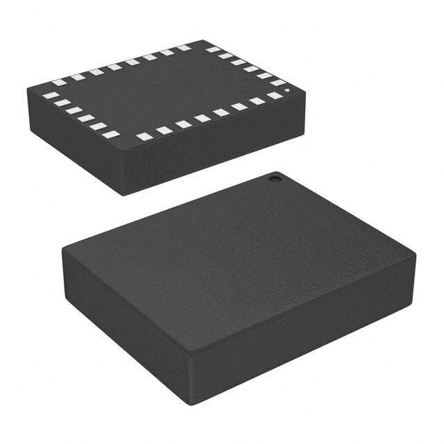
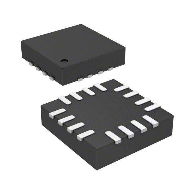
ICGOO电子元器件商城为您提供ADXRS450BEYZ由Analog设计生产,在icgoo商城现货销售,并且可以通过原厂、代理商等渠道进行代购。 ADXRS450BEYZ价格参考¥449.68-¥449.68。AnalogADXRS450BEYZ封装/规格:运动传感器 - 陀螺仪, Gyroscope X (Pitch), Y (Roll), Z (Yaw) ±300 80Hz SPI 14-CLCC (9x9)。您可以下载ADXRS450BEYZ参考资料、Datasheet数据手册功能说明书,资料中有ADXRS450BEYZ 详细功能的应用电路图电压和使用方法及教程。
ADXRS450BEYZ 是由 Analog Devices Inc.(ADI)生产的一款运动传感器 - 陀螺仪,其应用场景广泛,尤其适合需要高精度角速度测量的领域。以下是该型号的主要应用场景:

1. 导航系统
   ADXRS450BEYZ 可用于惯性导航系统(INS)中,提供精确的角速度数据以辅助 GPS 定位。在车辆、无人机或飞行器导航中,它能够补偿 GPS 信号丢失时的方向信息,确保设备保持正确的航向。

2. 工业自动化
   在工业机器人和自动化设备中,该陀螺仪可用于监测和控制机械臂或其他运动部件的姿态与方向,从而提高操作精度和稳定性。

3. 消费电子设备
   适用于游戏控制器、虚拟现实(VR)/增强现实(AR)头显等设备,用于追踪用户的头部或手部动作,实现更自然的人机交互体验。

4. 航空航天与国防
   在导弹制导、飞机稳定控制系统以及卫星姿态控制等领域,ADXRS450BEYZ 提供了可靠的角速度测量能力,帮助维持飞行器或航天器的稳定性。

5. 医疗设备
   该陀螺仪可以集成到康复设备、步态分析仪器或平衡训练装置中,用于实时监测患者的运动状态并提供反馈。

6. 汽车电子
   在汽车电子稳定控制系统(ESC)、防滚翻系统和自动驾驶技术中,ADXRS450BEYZ 能够检测车辆的旋转角度,防止侧翻或失控。

7. 无人机与无人车
   为无人机和无人车提供稳定性和方向控制支持,确保其在复杂环境中的正常运行。

总结来说,ADXRS450BEYZ 凭借其高性能、低噪声和宽工作温度范围的特点,成为众多对精度和可靠性要求较高的应用领域的理想选择。
| 参数 | 数值 |
| 产品目录 | |
| 描述 | SENS GYRO 300DEG/S DGTL 14CLCC螺旋仪 Hi Vibrate 300 Deg/s Immunity Digital |
| 产品分类 | 陀螺仪运动与定位传感器 |
| 品牌 | Analog Devices Inc |
| 产品手册 | |
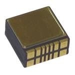
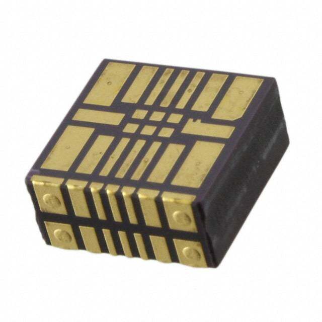
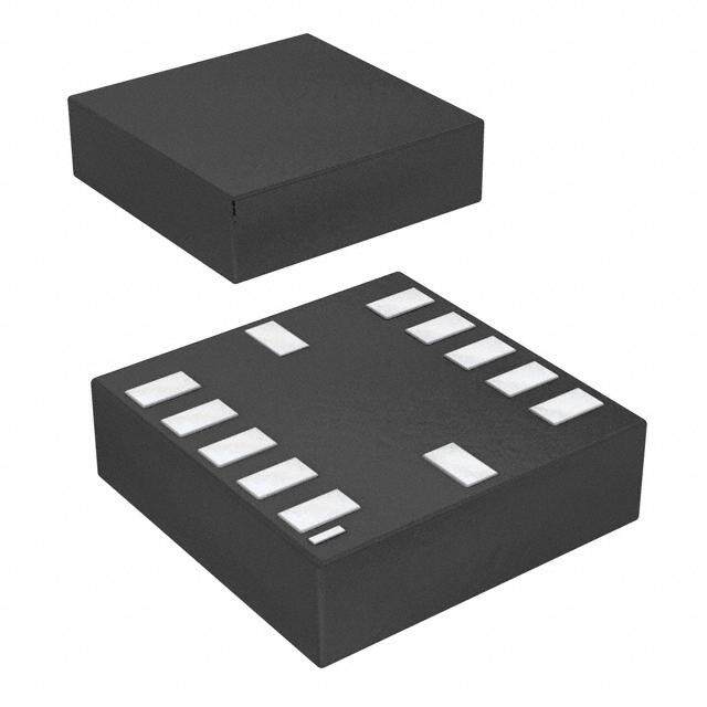
| 产品图片 |
|
| rohs | RoHS 合规性豁免无铅 / 符合限制有害物质指令(RoHS)规范要求 |
| 产品系列 | 螺旋仪,Analog Devices ADXRS450BEYZ- |
| 数据手册 | |
| 产品型号 | ADXRS450BEYZ |
| PCN组件/产地 | |
| PCN设计/规格 | |
| 产品种类 | 螺旋仪 |
| 传感轴 | Z |
| 供应商器件封装 | 14-CLCC(9x9) |
| 典型带宽 | 80Hz |
| 加速 | 2000 g |
| 商标 | Analog Devices |
| 宽度 | 9.2 mm |
| 封装 | Tube |
| 封装/外壳 | 14-CLCC |
| 封装/箱体 | LCCV-14 |
| 工作温度 | -40°C ~ 105°C |
| 工厂包装数量 | 32 |
| 带宽 | 80 Hz |
| 数字输出-位数 | 16 bit |
| 数字输出-总线接口 | SPI |
| 最大工作温度 | + 105 C |
| 最小工作温度 | - 40 C |
| 标准包装 | 1 |
| 灵敏度 | 80LSB/°/s |
| 电压-电源 | 3.15 V ~ 5.25 V |
| 电流-电源 | 6mA |
| 电源电压-最大 | 5.25 V |
| 电源电压-最小 | 3.15 V |
| 电源电流 | 6 mA |
| 系列 | ADXRS450 |
| 线性 | 99.75 % |
| 范围 | +/- 300 deg/s |
| 范围°/s | ±300°/s |
| 输出类型 | SPI |
| 长度 | 9.2 mm |
| 高度 | 4.4 mm |


- 商务部:美国ITC正式对集成电路等产品启动337调查
- 曝三星4nm工艺存在良率问题 高通将骁龙8 Gen1或转产台积电
- 太阳诱电将投资9.5亿元在常州建新厂生产MLCC 预计2023年完工
- 英特尔发布欧洲新工厂建设计划 深化IDM 2.0 战略
- 台积电先进制程称霸业界 有大客户加持明年业绩稳了
- 达到5530亿美元!SIA预计今年全球半导体销售额将创下新高
- 英特尔拟将自动驾驶子公司Mobileye上市 估值或超500亿美元
- 三星加码芯片和SET,合并消费电子和移动部门,撤换高东真等 CEO
- 三星电子宣布重大人事变动 还合并消费电子和移动部门
- 海关总署:前11个月进口集成电路产品价值2.52万亿元 增长14.8%

PDF Datasheet 数据手册内容提取
High Performance, Digital Output Gyroscope Data Sheet ADXRS450 FEATURES GENERAL DESCRIPTION Complete rate gyroscope on a single chip The ADXRS450 is an angular rate sensor (gyroscope) intended ±300°/sec angular rate sensing for industrial, medical, instrumentation, stabilization, and other High vibration rejection over a wide frequency range high performance applications. An advanced, differential, quad Excellent 25°/hour null offset stability sensor design rejects the influence of linear acceleration, enabling 2000 g powered shock survivability the ADXRS450 to operate in exceedingly harsh environments SPI digital output with 16-bit data-word where shock and vibration are present. Low noise and low power The ADXRS450 uses an internal, continuous self-test archi- 3.3 V and 5 V operation tecture. The integrity of the electromechanical system is checked −40°C to +105°C operation by applying a high frequency electrostatic force to the sense Ultrasmall, light, and RoHS compliant structure to generate a rate signal that can be differentiated from Two package options the baseband rate data and internally analyzed. Low cost SOIC_CAV package for yaw rate (Z-axis) response Innovative ceramic vertical mount package, which can be The ADXRS450 is capable of sensing angular rate of up to oriented for pitch, roll, or yaw response ±300°/sec. Angular rate data is presented as a 16-bit word, as part of a 32-bit SPI message. APPLICATIONS The ADXRS450 is available in a cavity plastic 16-lead SOIC Rotation sensing medical applications (SOIC_CAV) and an SMT-compatible vertical mount package Rotation sensing industrial and instrumentation (LCC_V), and is capable of operating across both a wide voltage High performance platform stabilization range (3.3 V to 5 V) and temperature range (−40°C to +105°C). FUNCTIONAL BLOCK DIAGRAM CP5 VX HGIGEHN EVROALTTIAOGNE ADXRS450 PDD LDO REGULATOR DVDD HV DRIVE AVDD CLOCK ALU PHASE- DIVIDER LOCKED LOOP AMPLITUDE DECFIILMTAETRION RY DETECT O M TEMPERATURE ME MOSI BAFNIDLT-PEARSS ADC 12 DEMOD CALIBRATION ERS/ INTESRPFIACE MSCISLOK T GIS CS Q DAQ Q FILTER DEFTAEUCLTTION RE Z-AXIS ANGULAR RATE SENSOR P DAQ CONSTTROL DVSS PSS AVSS EEPROM 08952-001 Figure 1. Rev. C Document Feedback Information furnished by Analog Devices is believed to be accurate and reliable. However, no responsibility is assumed by Analog Devices for its use, nor for any infringements of patents or other One Technology Way, P.O. Box 9106, Norwood, MA 02062-9106, U.S.A. rights of third parties that may result from its use. Specifications subject to change without notice. No license is granted by implication or otherwise under any patent or patent rights of Analog Devices. Tel: 781.329.4700 ©2011–2013 Analog Devices, Inc. All rights reserved. Trademarks and registered trademarks are the property of their respective owners. Technical Support www.analog.com
ADXRS450 Data Sheet TABLE OF CONTENTS Features .............................................................................................. 1 Mechanical Considerations for Mounting .............................. 10 Applications ....................................................................................... 1 Applications Circuits ................................................................. 10 General Description ......................................................................... 1 ADXRS450 Signal Chain Timing ............................................. 10 Functional Block Diagram .............................................................. 1 SPI Communication Protocol ....................................................... 12 Revision History ............................................................................... 2 Command/Response ................................................................. 12 Specifications ..................................................................................... 3 SPI Communications Characteristics ...................................... 13 Absolute Maximum Ratings ............................................................ 4 SPI Applications ......................................................................... 14 Thermal Resistance ...................................................................... 4 SPI Rate Data Format ..................................................................... 19 Rate Sensitive Axis ....................................................................... 4 Memory Map and Registers .......................................................... 20 ESD Caution .................................................................................. 4 Memory Map .............................................................................. 20 Pin Configuration and Function Descriptions ............................. 5 Memory Register Definitions ................................................... 21 Typical Performance Characteristics ............................................. 7 Package Orientation and Layout Information ............................ 23 Theory of Operation ........................................................................ 9 Package Marking Codes ............................................................ 25 Continuous Self-Test .................................................................... 9 Outline Dimensions ....................................................................... 26 Applications Information .............................................................. 10 Ordering Guide .......................................................................... 27 REVISION HISTORY 5/13—Rev. B to Rev. C Changes to Features Section............................................................ 1 Changed Null Accuracy from ±3°/sec to ±6°/sec......................... 3 Deleted Figure 6 from Low-Pass Filter Cut-Off (−3 dB) Frequency Test Conditions/Comments and Figure 7 from ST Low-Pass Filter −3 dB Frequency Test Conditions/Comments.... 3 Changes to Figure 6, Figure 7, and Figure 11 ............................... 7 Deleted Figure 10; Renumbered Sequentially............................... 7 Deleted Figure 13 and Figure 15 ..................................................... 8 Added Figure 12; Renumbered Sequentially ................................ 8 Changes to Figure 13 and Figure 15 ............................................... 8 Deleted Calibrated Performance Section .................................... 10 Changes to Applications Circuits Section ................................... 11 Changes to Figure 25 ...................................................................... 18 Changed Heading in Table 14 to 16-Bit Rate Data .................... 19 Updated Outline Dimensions ....................................................... 26 12/11—Rev. A to Rev. B Changes to the Rate Sensitive Axis Section .................................. 4 Changes to Figure 5 .......................................................................... 6 Changes to Figure 28 ...................................................................... 23 Deleted Figure 31, Renumbered Sequentially............................. 24 Changes to Back Side Terminals Notation, Figure 34 ............... 26 6/11—Rev. 0 to Rev. A Changes to Ordering Guide .......................................................... 28 1/11—Revision 0: Initial Version Rev. C | Page 2 of 28
Data Sheet ADXRS450 SPECIFICATIONS Specification conditions @ T = T to T , P = 5 V, angular rate = 0°/sec, bandwidth = 80 Hz ±1 g, continuous self-test on. A MIN MAX DD Table 1. Parameter Test Conditions/Comments Symbol Min Typ Max Unit MEASUREMENT RANGE Full-scale range FSR ±300 ±400 °/sec SENSITIVITY See Figure 2 Nominal Sensitivity 80 LSB/°/sec Sensitivity Tolerance ±3 % Nonlinearity1 Best fit straight line 0.05 0.25 % FSR rms Cross Axis Sensitivity2 ±3 % NULL Null Accuracy ±6 °/sec NOISE PERFORMANCE Rate Noise Density T = 25°C 0.015 °/sec/√Hz A LOW-PASS FILTER Cut-Off (−3 dB) Frequency f/200 f 80 Hz 0 LP Group Delay3 f = 0 Hz t 3.25 4 4.75 ms LP SHOCK AND VIBRATION IMMUNITY Sensitivity to Linear Acceleration DC to 5 kHz 0.03 °/sec/g Vibration Rectification 0.003 °/sec/g2 SELF TEST See Continuous Self-Test section Magnitude 2559 LSB Fault Register Threshold Compared to LOCST data 2239 2879 LSB Sensor Data Status Threshold Compared to LOCST data 1279 3839 LSB Frequency f/32 f 500 Hz 0 ST ST Low-Pass Filter −3 dB Frequency f/800 2 Hz 0 Group Delay3 52 64 76 ms SPI COMMUNICATIONS Clock Frequency 8.08 MHz Voltage Input High MOSI, CS, SCLK 0.85 × PDD PDD + 0.3 V Voltage Input Low MOSI, CS, SCLK −0.3 PDD × 0.15 V Output Voltage Low MISO, current = 3 mA 0.5 V Output Voltage High MISO, current = −2 mA P − 0.5 V DD Pull-Up Current CS, P = 3.3 V, CS = 0.75 × P 50 200 µA DD DD CS, P = 5 V, CS = 0.75 × P 70 300 µA DD DD MEMORY REGISTERS See the Memory Register Definitions section Temperature Sensor Value at 45°C 0 LSB Scale Factor 5 LSB/°C Quad, ST, Rate, DNC Registers Scale Factor 80 LSB/°/sec POWER SUPPLY Supply Voltage P 3.15 5.25 V DD Quiescent Supply Current I 6.0 10.0 mA DD Turn-On Time Power on to 0.5°/sec of final 100 ms TEMPERATURE RANGE Independent of package type T , T −40 +105 °C MIN MAX 1 Maximum limit is guaranteed through Analog Devices, Inc., characterization. 2 Cross axis sensitivity specification does not include effects due to device mounting on a printed circuit board (PCB). 3 Minimum and maximum limits are guaranteed by design. Rev. C | Page 3 of 28
ADXRS450 Data Sheet ABSOLUTE MAXIMUM RATINGS RATE SENSITIVE AXIS Table 2. Parameter Rating The ADXRS450 is available in two package options. The Acceleration (Any Axis, 0.5 ms) SOIC_CAV package configuration is for applications that Unpowered 2000 g require a z-axis (yaw) rate sensing device. Powered 2000 g The vertical mount package (LCC_V) option is for applications Supply Voltage (PDD) −0.3 V to +6.0 V that require rate sensing in the axes parallel to the plane of the Output Short-Circuit Duration (Any Pin to Indefinite PCB (pitch and roll). See Figure 2 for details. Ground) RATE Temperature Range AXIS Z-AXIS Operating LCC_V Package −40°C to +125°C + SOIC_CAV Package −40°C to +125°C Storage 16 LSCOCIC__VC PAaVc kPaagcek age −−6450°°CC ttoo ++115500°°CC SOIC PACKAGE9 RAAXTISE LCC_V PA+CKAGE 08952-002 Stresses above those listed under Absolute Maximum Ratings Figure 2. Rate Signal Increases with Clockwise Rotation may cause permanent damage to the device. This is a stress The LCC_V package has terminals on two faces; however, the rating only; functional operation of the device at these or any terminals on the back side are for internal evaluation only and other conditions above those indicated in the operational should not be used in the end application. The terminals on the section of this specification is not implied. Exposure to absolute bottom of the package incorporate metallization bumps that maximum rating conditions for extended periods may affect ensure a minimum solder thickness for improved solder joint device reliability. reliability. These bumps are not present on the back side THERMAL RESISTANCE terminals and, therefore, poor solder joint reliability can be encountered if used in the end application. See Figure 32 in the θ is specified for the worst-case conditions, that is, for a device JA Outline Dimensions section for a schematic of the LCC_V soldered in a printed circuit board (PCB) for surface-mount package. packages. ESD CAUTION Table 3. Thermal Resistance Package Type θ θ Unit JA JC 16-Lead SOIC_CAV 191.5 25 °C/W 14-Lead Ceramic LCC_V 185.5 23 °C/W Rev. C | Page 4 of 28
Data Sheet ADXRS450 PIN CONFIGURATION AND FUNCTION DESCRIPTIONS DVDD 1 16 SCLK RSVD 2 15 MOSI RSVD 3 14 AVDD ADXRS450 CS 4 TOP VIEW 13 DVSS MISO 5 (Not to Scale) 12 RSVD PDD 6 11 AVSS PSS 7 10 RSVD VX 8 9 CP5 08952-003 Figure 3. SOIC_CAV Pin Configuration Table 4. 14-Lead SOIC_CAV Pin Function Descriptions Pin No. Mnemonic Description 1 DV Digital Regulated Voltage. See Figure 19 for the applications circuit diagram. DD 2 RSVD Reserved. This pin must be connected to DV . SS 3 RSVD Reserved. This pin must be connected to DV . SS 4 CS Chip Select. 5 MISO Master In/Slave Out. 6 P Supply Voltage. DD 7 P Switching Regulator Ground. SS 8 VX High Voltage Switching Node. See Figure 19 for the applications circuit diagram. 9 CP5 High Voltage Supply. See Figure 19 for the applications circuit diagram. 10 RSVD Reserved. This pin must be connected to DV . SS 11 AV Analog Ground. SS 12 RSVD Reserved. This pin must be connected to DV . SS 13 DV Digital Signal Ground. SS 14 AV Analog Regulated Voltage. See Figure 19 for the applications circuit diagram. DD 15 MOSI Master Out/Slave In. 16 SCLK SPI Clock. Rev. C | Page 5 of 28
ADXRS450 Data Sheet PDD PSS MOSI DVSS CS VX RSVD 14 13 12 11 10 9 8 1 2 3 4 5 6 7 S D O D K 5 D AVS AVD(NToMISOt Pto DVV DSIEcWaSCLle)CP RSV 08952-005 Figure 4. LCC_V Pin Configuration RSVD CP5 SCLKDVDDMISOAVDD AVSS 7 6 5 4 3 2 1 8 9 101112 13 14 RSVD VX CSDVSSMOSI PSS PDD (Not to Scale) NOTES 1. THE LCC_V PACKAGE HAS TWO TERMINALS ON TWO FACES; HOWEVER, THE TERMINALS ON THE BACK SIDE ARE FOR INTERNAL EVALUATION ONLY AND SHOULD NOT BE USED IN THE END APPLICATION. THE TERMINALS ON THE BOTTOM OF THE PACKAGE INCORPORATE METALLIZATION BUMPS THAT ENSURE A MINIMUM SOLDER THICKNESS FOR IMPROVED SOLDER JOINT RELIABILITY. THESE BUMPS ARE NOT PESRCNEHCSEOEMUNANTTT IEOCRN OE TDFH TIEFH BUEAS LCECKDC SI_NVID TPEHA TECE EKRNAMDGI NEAA.PLPSL IACNADT,I OTNH.E SREEEF OTRHEE, OPUOTOLRIN SEO DLIDMEERN SJOIOINNTS RSEELCITAIBOINL IFTOY RC AAN BE 08952-037 Figure 5. LCC_V Pin Configuration, Horizontal Layout Table 5. 14-Lead LCC_V Pin Function Descriptions Pin No. Mnemonic Description 1 AV Analog Ground. SS 2 AV Analog Regulated Voltage. See Figure 20 for the applications circuit diagram. DD 3 MISO Master In/Slave Out. 4 DV Digital Regulated Voltage. See Figure 20 for the applications circuit diagram. DD 5 SCLK SPI Clock. 6 CP5 High Voltage Supply. See Figure 20 for the applications circuit diagram. 7 RSVD Reserved. This pin must be connected to DV . SS 8 RSVD Reserved. This pin must be connected to DV . SS 9 VX High Voltage Switching Node. See Figure 20 for the applications circuit diagram. 10 CS Chip Select. 11 DV Digital Signal Ground. SS 12 MOSI Master Out/Slave In. 13 P Switching Regulator Ground. SS 14 P Supply Voltage. DD Rev. C | Page 6 of 28
Data Sheet ADXRS450 TYPICAL PERFORMANCE CHARACTERISTICS 20 40 18 35 16 30 N 14 N O O ATI 12 ATI 25 L L U U P 10 P 20 O O P P F 8 F O O 15 % % 6 10 4 2 5 0 –2.0 –1.6 –1.2 –0.8NUL–0.4L ERR0OR (°0.4/sec) 0.8 1.2 1.6 2.0 08952-006 0–2.0 –1.6 –1.2 –0.8NU–L0L.4 ERR0OR (0°/.s4ec)0.8 1.2 1.6 2.0 08952-009 Figure 6. SOIC_CAV Null Error @ 25°C Figure 9. LCC_V Null Error @ 25°C 30 25 25 20 ON 20 ON TI TI 15 A A L L U U P 15 P O O P P F F 10 O O % 10 % 5 5 0 0 –0.20–0.18–0.16N–0.14UL–0.12L T–0.10EM–0.08PE–0.06RA–0.04TU–0.02RE0 C0.02OE0.04FF0.06ICI0.08EN0.10T (°0.12/se0.14c/°0.16C)0.180.200.22 08952-007 –3.0 –2.5 –2.0 –1.5CHA–1.0NGE–0.5 IN SE0NSIT0.5IVITY1.0 (%)1.5 2.0 2.5 3.0 08952-029 Figure 7. SOIC_CAV Null Temperature Coefficient Figure 10. LCC_V Sensitivity Error @ 25°C 25 20 20 15 N N O O ATI 15 ATI L L U U P P 10 O O P P F 10 F O O % % 5 5 0 0 –3.0 –2.5 –2.0 –1.5CHA–1.0NGE–0.5 IN SE0NSIT0.5IVITY1.0 (%)1.5 2.0 2.5 3.0 08952-008 –0.08 –0.07 –0.06 –0.05 –0.04 S–0.03EN–0.02SIT–0.01IVIT0Y D0.01RIF0.02T (%0.03/°C0.04) 0.05 0.06 0.07 0.08 0.10 08952-112 Figure 8. SOIC_CAV Sensitivity Error @ 25°C Figure 11. SOIC_CAV Sensitivity Drift over Temperature Rev. C | Page 7 of 28
ADXRS450 Data Sheet 1 40 60 DUT1 30 DUT2 50 DUTAVERAGE (°/s) Hz) 0.1 20 REF 40 g) O OUTPUT (°/s/√ 0.01 O OUTPUT (°/s) 100 3200 CCELERATION ( GYR GYR –10 10 UT A P 0.001 –20 0 IN –30 –10 0.00015 10 FREQUENCY (Hz) 100 300 08952-031 –400.1 0.15 0.20 TIM0E. 2(5sec) 0.30 0.35 0.40–20 08952-034 Figure 12. DUT Typical Response to Random Vibration Figure 14. Typical Shock Response (5 Hz to 5 kHz at 15 g RMS) 8 86 6 84 4 (/sec)RIFT° 02 TY (LSB/°/sec) 8802 D VI L TI NUL –2 ENSI 78 S –4 76 –6 –8–50 –25 0 TEM2P5ERATUR50E(°C) 75 100 125 08952-114 74–50 –25 0 TEM2P5ERATUR50E (°C) 75 100 125 08952-117 Figure 13. Null Drift over Temperature Figure 15. Sensitivity over Temperature Rev. C | Page 8 of 28
Data Sheet ADXRS450 THEORY OF OPERATION CONTINUOUS SELF-TEST The ADXRS450 operates on the principle of a resonator gyro- scope. A simplified version of one of four polysilicon sensing The ADXRS450 gyroscope uses a complete electromechanical structures is shown in Figure 16. Each sensing structure contains self-test. An electrostatic force is applied to the gyroscope frame, a dither frame that is electrostatically driven to resonance. This resulting in a deflection of the capacitive sense fingers. This produces the necessary velocity element to produce a Coriolis deflection is exactly equivalent to deflection that occurs as a force when experiencing angular rate. In the SOIC_CAV package, result of external rate input. The output from the beam structure is the ADXRS450 is designed to sense a z-axis (yaw) angular rate; processed by the same signal chain as a true rate output signal, whereas the vertical mount package (LCC_V) orients the device providing complete coverage of the electrical and mechanical such that it can sense pitch or roll angular rate on the same PCB. components. When the sensing structure is exposed to angular rate, the The electromechanical self-test is performed continuously during resulting Coriolis force couples into an outer sense frame, operation at a rate higher than the output bandwidth of the which contains movable fingers that are placed between fixed device. The self-test routine generates equivalent positive and pickoff fingers. This forms a capacitive pickoff structure that negative rate deflections. This information can then be filtered senses Coriolis motion. The resulting signal is fed to a series of with no overall effect on the demodulated rate output. gain and demodulation stages that produce the electrical rate signal output. The quad sensor design rejects linear and angular acceleration, including external g-forces and vibration. This is achieved by mechanically coupling the four sensing structures such that external g-forces appear as common-mode signals that can be removed by the fully differential architecture RATE SIGNAL WITH CONTINUOUS SELF TEST SIGNAL. implemented in the ADXRS450. SCEOLMF PTAERSETD TA ATMBOPL LTEIHT LEUI MDSEIPT.E SICN.ITFEICRANTAILOLNY LOW FREQUENCY RATE INFORMATION. 08952-012 Figure 17. Continuous Self-Test Demodulation X The difference amplitude between the positive and negative Y self-test deflections is filtered to 2 Hz, and it is continuously Z monitored and compared to hardcoded self-test limits. If the measured amplitude exceeds these limits (listed in Table 1), one of two error conditions asserts depending on the magnitude of self-test error. For less severe self-test error magnitudes, the CST bit of the fault register is asserted; however, the status bits (ST[1:0]) in the sensor data response remain set to 0b01 for valid sensor data. For more severe self-test errors, the CST bit of the fault reg- ister is asserted, and the status bits (ST[1:0]) in the sensor data 08952-011 rthesrepsohnosled sa froer s beot ttho o0fb t0h0e sfeo rfa iinluvrael icdo nsednitsioorn sd. aItfa d. eTsairbelde, 1th leis utss ethr e Figure 16. Simplified Gyroscope Sensing Structure can access the self-test information by issuing a read command to the self-test memory register (Address 0x04). For more infor- The resonator requires 22.5 V (typical) for operation. Because mation about error reporting, see the SPI Communication Protocol only 5 V is typically available in most applications, a switching section. regulator is included on chip. Rev. C | Page 9 of 28
ADXRS450 Data Sheet APPLICATIONS INFORMATION MECHANICAL CONSIDERATIONS FOR MOUNTING 1 DVDD SCLK 16 1µF Mount the ADXRS450 in a location close to a hard mounting RSVD MOSI point of the PCB to the case. Mounting the ADXRS450 at an 1µF unsupported PCB location (that is, at the end of a lever, or in RSVD AVDD the middle of a trampoline), as shown in Figure 18, can result in GND CS DVSS apparent measurement errors because the gyroscope is subject 3.3VTO 5V MISO RSVD to the resonant vibration of the PCB. Locating the gyroscope near a hard mounting point helps to ensure that any PCB reson- PDD AVSS 1µF ances at the gyroscope are above the frequency at which harmful PSS RSVD aliasing with the internal electronics can occur. To ensure that 100nF VX CP5 aliased signals do not couple into the baseband measurement 470µH oracncguer,s daet sai gfnre tqhuee mncoyd uhlieg hwehre trheiann t 8h0e 0fi rHstz s. y stem level resonance GND >24V BDRIEOADKEDOWN GND 08952-014 Figure 19. Recommended Applications Circuit, SOIC_CAV Package GYROSCOPE PCB 3.3VTO 5V TOP VIEW 1 14 AVSS PDD MOUNTING POINTS 08952-013 1µF AVDD PSS 1µF Figure 18. Incorrectly Placed Gyroscope MISO MOSI APPLICATIONS CIRCUITS 1µF DVDD DVSS Figure 19 and Figure 20 show the recommended application circuits for the ADXRS450 gyroscope. These application circuits SCLK CS GND provide a connection reference for the available package types. 100nF CP5 VX Note that DVDD, AVDD, and PDD are individually connected to 470µH ground through 1 μF capacitors; do not connect these supplies GND RSVD RSVD together. Additionally, an external diode and inductor must be connected for proper operation of the internal shunt regulator. These components (listed in Table 6) allow for the internal reso- GND nSpateocri fdicraivtieo vnosl tsaegceti oton .r each its required level, as listed in the >24V BDRIEOADKEDOWN 08952-015 Figure 20. Recommended Applications Circuit, Ceramic LCC_V Package Table 6. Internal Shunt Regulator Components ADXRS450 SIGNAL CHAIN TIMING Component Qty. Description The ADXRS450 primary signal chain is shown in Figure 21; it is Inductor 1 470 μH the series of necessary functional circuit blocks through which Diode 1 >24 V breakdown voltage the rate data is generated and processed. This sequence of electro- Capacitor 3 1 μF mechanical elements determines how quickly the device is capable Capacitor 1 100 nF of translating an external rate input stimulus into an SPI word Note the following schematic recommendations: to be sent to the master device. The group delay, which is a func- • Keep leakage current on the CP5 pin to a minimum. tion of the filter characteristic, is the time required for the output All sources of leakage, including reverse leakage current of the low-pass filter to be within 10% of the external rate input, through the diode and PCB surface leakage should account and is seen to be ~4 ms. Additional delay can be observed due for not more than 70 μA. For most applications, the diode to the timing of SPI transactions and the population of the rate is the primary source of leakage current. data into the internal device registers. Figure 21 anatomizes this • Applications that operate at 3.3 V should use an inductor delay, wherein the delay through each element of the signal chain is presented. value of 560 μH to ensure proper operation of the internal boost regulator. For all applications, the inductor should be capable for 50 mA of peak current. Rev. C | Page 10 of 28
Data Sheet ADXRS450 The transfer function for the rate data LPF is given as The transfer function for the continuous self-test LPF is given as 1Z642 1 1Z1 6463Z1 where: where: 16 1 1 T = 1ms(typ) T = f f 16kHz(typ) 0 0 PRIMARY SIGNAL CHAIN 4ms GROUP DELAY <2.2ms ARITHMETIC DELAY <5µs <5µs <5µs LOGIC UNIT RY DELAY DELAY DELAY O M E M BAFNILDT-PEARSS ADC 12 DEMOD RATLEP DFATA TERS/ TRANSSAPCITION S GI E CONTINUOUS R Z-AXIS ANGULAR SELF-TEST RATE SENSOR LPF GRO<U6P4 mDEsLAY 08952-016 Figure 21. Primary Signal Chain and Associated Delays Rev. C | Page 11 of 28
ADXRS450 Data Sheet SPI COMMUNICATION PROTOCOL COMMAND/RESPONSE Table 7. SPI Signals Input/output is handled through a 32-bit, command/response Signal Symbol Description SPI interface. The command set and the format for the interface Serial Clock SCLK Exactly 32 clock cycles during CS active is defined as follows: Chip Select CS Active low Clock phase = clock polarity = 0 Master Out MOSI Data sent to the gyroscope device Additionally, the device response to the initial command is Slave In from the main controller 0x00000001. This prevents the transmission of random data to Master In MISO Data sent to the main controller the master device upon the initial command/response exchange. Slave Out from the gyroscope CS 32 CLOCK 32 CLOCK CYCLES CYCLES SCLK MOSI COMMAND N COMMAND N + 1 MISO RESPONSE N – 1 RESPONSE N 08952-017 Figure 22. SPI Protocol Table 8. SPI Commands Bit Command 31 30 29 28 27 26 25 24 23 22 21 20 19 18 17 16 15 14 13 12 11 10 9 8 7 6 5 4 3 2 1 0 Sensor SQ1 SQ0 1 SQ2 CHK P Data Read 1 0 0 SM2 SM1 SM0 A8 A7 A6 A5 A4 A3 A2 A1 A0 P Write 0 1 0 SM2 SM1 SM0 A8 A7 A6 A5 A4 A3 A2 A1 A0 D15 D14 D13 D12 D11 D10 D9 D8 D7 D6 D5 D4 D3 D2 D1 D0 P Table 9. SPI Responses Bit Command 31 30 29 28 27 26 25 24 23 22 21 20 19 18 17 16 15 14 13 12 11 10 9 8 7 6 5 4 3 2 1 0 Sensor SQ2 SQ1 SQ0 P0 ST1 ST0 D15 D14 D13 D12 D11 D10 D9 D8 D7 D6 D5 D4 D3 D2 D1 D0 PLL Q NVM POR PWR CST CHK P1 Data Read 0 1 0 P0 1 1 1 0 SM2 SM1 SM0 D15 D14 D13 D12 D11 D10 D9 D8 D7 D6 D5 D4 D3 D2 D1 D0 P1 Write 0 0 1 P0 1 1 1 0 SM2 SM1 SM0 D15 D14 D13 D12 D11 D10 D9 D8 D7 D6 D5 D4 D3 D2 D1 D0 P1 R/W 0 0 0 P0 1 1 1 0 SM2 SM1 SM0 0 0 SPI RE DU PLL Q NVM POR PWR CST CHK P1 Error Rev. C | Page 12 of 28
Data Sheet ADXRS450 SPI COMMUNICATIONS CHARACTERISTICS Table 10. SPI Command/Response Timing Characteristics Note the following conditions for Table 10: Symbol Description Min Max Unit f SPI operating 8.08 MHz • All minimum and maximum timing values are guaranteed OP frequency through characterization. t Clock (SCLK) 1/2t − 13 ns SCLKH SCLK • All timing is shown with respect to 10% VDD and 90% of high time the actual delivered voltage waveform. tSCLKL Clock (SCLK) low 1/2tSCLK − 13 ns • All minimum and maximum timing values are valid for time t SCLK period 123.7 ns 3.0 V ≤ V ≤ 5.5 V. SCLK DD t Clock (SCLK) fall 5.5 13 ns • Capacitive load for all signals is assumed to be ≤80 pF. F time • Ambient temperature is −40°C ≤ TA ≤ +105°C. tR Clock (SCLK) rise 5.5 13 ns • MISO pull-up of 47 kΩ or 110 µA. time • Sequential transfer increases to 17 ms following any write tSU Data input 37 ns (MOSI) setup operation limited by the EEPROM. time tHIGH Data input 49 ns (MOSI) hold time t Data output 20 ns A (MISO) access time t Data output 20 ns V (MISO) valid after SCLK t Data output 0 ns LAG (MISO) lag time t Data output 40 ns DIS (MISO) disable time tLEAD Enable (CS) lead 1/2tSCLK ns time tLAG Enable (CS) lag 1/2tSCLK ns time t Sequential 0.1 ms D transfer delay f Gyroscope 13 19 kHz 0 resonant frequency Rev. C | Page 13 of 28
ADXRS450 Data Sheet SPI APPLICATIONS appropriate data is shifted into the SPI port registers in prepara- Device Data Latching tion for the next sequential command/response exchange. This allows for an exceedingly fast sequential transfer delay of 0.1 ms To allow for rapid acquisition of data from the ADXRS450, (see Table 10). As a design precaution, note that the transmitted device data latching has been implemented in the design, as shown data is only as recent as the sequential transmission delay imple- in Figure 24. Upon the assertion of chip select (CS), the data mented by the system. Conditions that result in a sequential present in the device is latched into memory. When the full transfer delay of several seconds cause the next sequential device MOSI command has been received, and CS deasserted, the response to contain data that is several seconds old. CS tSCLK tLEAD tSCLKH tSCLKL tF tR tLAG tD SCK tA tV tLAG tDIS MISO MSB LSB tHIGH tSU MOSI MSB LSB 08952-018 Figure 23. SPI Timings DEVICE DATA IS LATCHED AFTER THE ASSERTION OF CS. LATCHED DATA IS TRANSMITTED DURING THE NEXT SEQUENTIAL COMMAND/RESPONSE EXCHANGE. CS 32 CLOCK 32 CLOCK 32 CLOCK SCLK CYCLES CYCLES CYCLES MOSI COMMAND N COMMAND N + 1 COMMAND N + 2 0x… 0x… 0x… MISO RE0SxP0O0N00S0E0 0N1 – 1 RESP0Ox…NSE N RESPO0Nx…SE N + 1 08952-019 Figure 24. Device Data Latching Rev. C | Page 14 of 28
Data Sheet ADXRS450 Command/Response—Bit Definitions ST1 to ST0 Table 11. Quick Guide—Bit Definitions for SPI Interface The status bits (ST1 and ST0) are used to signal to the master Bit Description device the type of data contained in the response message. The status bits are decoded as listed in Table 12. SQ2 to SQ0 Sequence bits (from master) SM2 to SM0 Sensor module bits (from master) Table 12. Status Bit Code Definitions A8 to A0 Register address ST1:ST0 Content in Bits[D15:D0] D15 to D0 Data 00 Error data for sensor data response SPI SPI command/response 01 Valid sensor data ST1 to ST0 Status bits 10 Sensor self-test data P Command odd parity 11 Read/write response P0 Response, odd parity, Bits[31:16] P1 Response, odd parity, Bits[31:0] There are two independent conditions that can result in the ST RE Request error bits being set to 0b00 during a sensor data response: self-test or DU Data unavailable PLL. The self-test response is sufficiently different from its nominal value. Refer to the Specifications section for the appropriate limits. SQ2 to SQ0 When the sensor data response is a PLL, the PLL fault is active. This field provides the system with a means of synchronizing the data samples that are received from multiple sensors. To P facilitate correct synchronization, the ADXRS450 gyroscope A parity bit (P) is required for all master-to-slave data transmis- includes the SQ[2:0] field in the response sequence as it was sions. Communications protocol requires one parity bit to achieve received in the request. odd parity for the entire 32-bit command. Bits that are in don’t care positions remain factored into the parity calculation. SM2 to SM0 P0 Sensor module bits from master device. These bits have not been implemented in the ADXRS450, and are hardcoded to be P0 is the parity bit that establishes odd parity for Bits[31:16] of 000 for all occurrences. the device response. A8 to A0 P1 The A8 to A0 bits represent the memory address from which P1 is the parity bit that establishes odd parity for the entire device data is being read, or to which information is to be written. 32-bit device response. These bits should only be supplied by the master when the RE memory registers are being accessed, and are ignored for all RE is the communications error bit transmitted from the sensor data requests. Refer to the Memory Register Definitions ADXRS450 device to the control module. Request errors (RE) section for a complete description of the available memory can occur when registers. • An invalid command is sent from the control module. D15 to D0 • The read/write command specifies an invalid memory 16-bit device data that can contain any of the following: register. • Master—data to be written to a memory register as • The write command attempted to a nonwriteable memory specified in the A8 to A0 section. register. • Slave—sensor rate output data. • Slave—device data read from the memory register DU specified in the A8 to A0 section, as well as the data from As expressed in Table 10, the sequential transfer delay for the next sequential register. writing data to a memory register (for example, DNC0) results • Slave—for a write command, the 16-bit data that is written in a sequential transfer delay of 0.1 ms. If a successive write to the specified memory register reflects back to the master command is issued to the device prior to the completion of the device for correlation. sequential transfer delay, the command is ignored and the device issues a data unavailable (DU) error response. However, a read SPI command or sensor data request can be issued after a sequential The SPI bit sets when any of the following occurs: either too transfer delay of only 10 µs is observed. Regardless of the com- many/not enough bits are transmitted, or the message from the mands that are subsequently issued to the device, when a write control module contains a parity error. Additionally, any error procedure has been initiated, the operation proceeds through to during a sensor data request results in the device issuing a completion (requiring 17 ms). read/write error. Rev. C | Page 15 of 28
ADXRS450 Data Sheet Fault Register Bit Definitions POR This section describes the bits available for signaling faults to An internal check is performed at the time of device startup to the user. The individual bits of the fault register are updated ensure that the volatile memory of the device is functional. This asynchronously depending on their respective detection criteria; is accomplished by programming a known value from the device however, it is recommended that the fault register be read at a ROM into a volatile memory register. This value is then conti- rate of at least 250 Hz. When asserted, the individual status bit nuously compared to the known value in ROM every 1 µs for the does not deassert until it is read by the master device. If the duration of device operation. If the value stored in the volatile error persists after a fault register read, the status bit immediately memory changes, or does not match the value stored in ROM, reasserts, and remains asserted until the next sequential command/ the POR error flag is asserted. The value stored in ROM is response exchange. The full fault register is appended to every rewritten to the volatile memory upon a device power cycle. sensor data request. It can also be accessed by issuing a read PWR command to Register 0x0A. The device performs a continuous check of the internal 3 V regulated voltage level. If either an overvoltage (OV) or under- Table 13. Quick Guide—Fault Register Bit Definitions voltage (UV) fault is asserted, then the power (PWR) bit is also Bit Name Description asserted. This condition occurs if the regulated voltage is observed PLL PLL failure to be either above 3.3 V or below 2.77 V. An internal low-pass filter Q Quadrature error removes high frequency glitching effects to prevent the PWR bit NVM Nonvolatile memory fault (NVM) from asserting unnecessarily. To determine if the fault is a result of POR Power-on reset failed to initialize an overvoltage or undervoltage condition, the OV and UV fault UV Regulator undervoltage bits must be analyzed. Amp Amplitude detection failure PWR Power regulation failed: overvoltage/undervoltage CST CST Continuous self-test failure The ADXRS450 is designed with continuous self-test (CST) CHK Check: generate faults functionality. Measured self-test amplitudes are compared OV Regulator overvoltage against the limits presented in Table 1. Deviations from this Fail Failure that sets the ST[1:0] bits to 0b00 value are what result in reported self-test errors. There are two thresholds for a self-test failure. PLL PLL is the bit indicating that the device has had a failure in the • Self-test value > ±512 LSB from nominal results in an phase-locked loop functional circuit block. This occurs when assertion of the self-test flag in the fault register. the PLL has failed to achieve sync with the resonator structure. • Self-test value > ±1856 LSB from nominal results in both an If the PLL status flag is active, the ST bits of the sensor data assertion of the self-test flag in the fault register as well as response are set to 0b00, indicating that the response contains setting the ST[1:0] bits to 0b00, indicating that the rate data potentially invalid rate data. contained in the sensor data response is potentially invalid. Q CHK A Q fault can be asserted based on two independent quadrature The control module transmits the check (CHK) bit to the calculations. Located in the quad memory (Register 0x08) is a ADXRS450 as a method of generating faults. By asserting value corresponding to the total instantaneous quadrature present the CHK bit, the device creates conditions that result in the in the device. If this value exceeds 4096 LSB, a Q fault is issued. generation of all faults represented through the fault register. Because quadrature build-up can contribute to an offset error, For example, the self-test amplitude is deliberately altered to the ADXRS450 has integrated methods for dynamically cancelling exceed the fault detection threshold, resulting in a self-test the effects of quadrature. An internal quadrature accumulator error. In this way, the device is capable of checking both its records the amount of quadrature correction performed by the ability to detect a fault condition, as well as its ability to report ADXRS450. Excessive quadrature is associated with offset errors. that fault to the control module. A Q fault is issued when the quadrature error (Q) present in the The fault conditions are initiated nearly simultaneously; however, device has contributed to an equivalent of 4°/sec (typical) of rate the timing for receiving fault codes when the CHK bit is asserted is offset. dependent upon the time required to generate each unique fault. It NVM takes no more than 50 ms for all of the internal faults to be generated An NVM error transmits to the control module when the and for the fault register to be updated to reflect the condition of internal NVM data fails a checksum calculation. This check is the device. Until the CHK bit is cleared, the status bits (ST[1:0]) are performed once every 50 µs, and does not include the DNC0 or set to 0b10, indicating that the data should be interpreted by the PID memory registers. control module as self-test data. After the CHK bit is deasserted, the fault conditions require an additional 50 ms to decay, and the device to return to normal operation. Rev. C | Page 16 of 28
Data Sheet ADXRS450 OV Amp The overvoltage (OV) fault bit asserts if the internally regulated The amp fault bit is asserted when the measured amplitude of voltage (nominally 3 V) is observed to exceed 3.3 V. This measure- the silicon resonator has been significantly reduced. This con- ment is low-pass filtered to prevent artifacts such as noise spikes dition can occur if the voltage supplied to CP5 has fallen below from asserting a fault condition. When an OV fault has occurred, the requirements of the internal voltage regulator. This fault bit the PWR fault bit is asserted simultaneously. Because the OV is OR’ed with the CST fault such that during a sensor data request, fault bit is not transmitted as part of a sensor data request, it is the CST bit position represents either an amp failure or a CST recommended that the user read back the FAULT1 and FAULT0 failure. The full status register can then be read from memory to memory registers upon the assertion of a PWR error. This validate the specific failure. allows the user to determine the specific error condition. K-Bit Assertion: Recommended Start-Up Routine UV Figure 25 illustrates a recommended start-up routine that can The undervoltage (UV) fault bit asserts if the internally regu- be implemented by the user. Alternate start-up sequences can be lated voltage (nominally 3 V) is observed to be less than 2.77 V. employed; however, ensure that the response from the ADXRS450 This measurement is low-pass filtered to prevent artifacts such is handled correctly. If implemented immediately after power is as noise spikes from asserting a fault condition. When a UV applied to the device, the total time to implement the following fault has occurred, the PWR fault bit is asserted simultaneously. fault detection routine is approximately 200 ms. As the UV fault bit is not transmitted as part of a sensor data As described in the Device Data Latching section, the data present request, it is recommended that the user read back the FAULT1 in the device upon the assertion of the CS signal is used in the and FAULT0 memory registers upon the assertion of a PWR next sequential command/response exchange. This results in error. This allows the user to determine the specific error an apparent one transaction delay before the data resulting from condition. the assertion of the CHK command is reported by the device. Fail For all other read/write interactions with the device, no such The fail flag is asserted when a condition arises such that the delay exists, and the MOSI command is serviced during the ST[0:1] bits are set to 0b00. This indicates that the device has next sequential command/response exchange. Note that when experienced a gross failure, and that the sensor data could the CHK bit is deasserted, if the user tries to obtain data from potentially be invalid. the device before the CST fault flag has cleared, the device reports the data as error data. Rev. C | Page 17 of 28
ADXRS450 Data Sheet MOSI: SENSOR DATA REQUEST MOSI: SENSOR DATA MOSI: SENSOR DATA MOSI: SENSOR DATA CHK COMMAND ASSERTED REQUEST; CLEARS THE REQUEST REQUEST CHK BIT MISO: STANDARD INITIAL MISO: CHK RESPONSE MISO: CHK RESPONSE RESPONSE MISO: SENSOR DATA ST[1:0] = 0b10 ST[1:0] = 0b10 RESPONSE DATA LATCH POINT CS X X X 32 CLOCK 32 CLOCK 32 CLOCK 32 CLOCK SCLK CYCLES CYCLES CYCLES CYCLES MOSI 0x2000 0003 0x2000 0000 0x2000 0000 0x2000 0000 MISO 0x0000001 0x… (P0AxR…ITFYF D OERP E0xN…DEFNET) (P0AxR…ITFYF D OERP E0xN…DEFNET) t = 100ms t = 150ms t = 200ms t = 200ms +tTD t = 200ms + 2tTD POWER IS ONCE THE 100ms START-UP A 50ms DELAY IS REQUIRED ANOTHER 50ms DELAY MUST THE FAULT BITS OF THE ALL FAULT APPLIED TO TIME HAS OCCURRED, THE SO THAT THE GENERATION BE OBSERVED TO ALLOW ADXRS800 REMAIN ACTIVE CONDITIONS ARE THE DEVICE. MASTER DEVICE IS FREE TO OF FAULTS WITHIN THE THE FAULT CONDITIONS TO UNTIL CLEARED. DUE TO CLEARED, AND ALL WAIT 100ms TO ASSERT THE CHK BIT AND DEVICE IS ALLOWED TO CLEAR. IF THE DEVICE IS THE REQUIRED DECAY SUBSEQUENT DATA ALLOW FOR START THE PROCESS OF COMPLETE. HOWEVER, FUNCTIONING PROPERLY, PERIOD FOR EACH FAULT EXCHANGES NEED THE INTERNAL INTERNAL ERROR BECAUSE THE DEVICE DATA THE MISO RESPONSE CONDITION, FAULT ONLY OBSERVE CIRCUITRY TO CHECKING. DURING THE IS LATCHED BEFORE THE CONTAINS ALL ACTIVE CONDITIONS REMAIN THE SEQUENTIAL BE INITIALIZED. FIRST COMMAND/ CHK BIT IS ASSERTED, THE FAULTS, AS WELL AS HAVING PRESENT UPON THE TRANSFER DELAY RESPONSE EXCHANGE DEVICE RESPONSE DURING SET THE MESSAGE FORMAT IMMEDIATE DEASSERTION TIMING AFTER POWER-ON, THE THIS COMMAND/RESPONSE TO SELF-TEST DATA. THIS IS OF THE CHK BIT. THIS PARAMETER. ADXRS800 IS DESIGNED TO EXCHANGE DOES NOT INDICATED THROUGH THE ST RESULTS IN A SECOND ISSUE A PREDEFINED CONTAIN FAULT BITS BEING SET TO 0b10. SEQUENTIAL RESPONSE IN RESPONSE. INFORMATION. THIS WHICH THE FAULT BITS ARE RESPONSE CAN BE ASSERTED. AGAIN, THE DISCARDED. RESPONSE IS FORMATTED AIFINNASTDU ESICLNETALT TBFIOI-INTTNGSEA SLTHTLHA YDAV.ATE T TBAHEEEN SET 08952-020 Figure 25. Recommended Start-Up Sequence Rev. C | Page 18 of 28
Data Sheet ADXRS450 SPI RATE DATA FORMAT The ADXRS450 gyroscope transmits rate data in a 16-bit format, Therefore, the highest obtainable value for positive (clockwise) as part of a 32-bit SPI data frame. See Table 9 for the full 32-bit rotation is 0x7FFF (decimal +32,767), and for counterclockwise format of the sensor data request response. The rate data is trans- rotation is 0x8000 (decimal −32,768). Performance of the device mitted MSB first, from D15 to D0. The data is formatted as a is not guaranteed above ±24,000 LSB (±300°/sec). twos complement number, with a scale factor of 80 LSB/°/sec. Table 14. Rate Data 16-Bit Rate Data Decimal (LSBs) Hex (D15:D0) Data Type Description +32,767 0x7FFF Rate data (not guaranteed) Maximum possible positive data value … … … … +24,000 0x5DC0 Rate data +300 degrees per second rotation (positive FSR) … … … … +160 0x00A0 Rate data +2 degrees per second rotation +80 0x0050 Rate data +1 degree per second rotation … … … … +40 0x0028 Rate data +1/2 degree per second rotation +20 0x0014 Rate data +1/4 degree per second rotation … … … … 0 0x 0000 Rate data Zero rotation value … … … … −20 0xFFEC Rate data −1/4 degree per second rotation −40 0xFFD8 Rate data −1/2 degree per second rotation … … … … −80 0xFFB0 Rate data −1 degree per second rotation −160 0xFF60 Rate data −2 degree per second rotation … … … … −24,000 0xA240 Rate data −300 degree per second rotation (negative FSR) … … … … −32,768 0x8000 Rate data (not guaranteed) Maximum possible negative data value Rev. C | Page 19 of 28
ADXRS450 Data Sheet MEMORY MAP AND REGISTERS MEMORY MAP from the next, sequential register to the memory address that was specified. Data is transmitted MSB first. For proper acquisition of The following is a list of the memory registers that are available data from the memory register, make the read request to the even to be read from or written to by the customer. See the previous numbered register address only. Following the memory map section SPI Communication Protocol for the proper input (see Table 15) is the explanation of the significance of each sequence to read/write a specific memory register. Each memory register. memory register is comprised of eight bits of data, however, when a read request is performed, the data always returns as a 16-bit message. This is accomplished by appending the data Table 15. Memory Register Map Address Register Name MSB D6 D5 D4 D3 D2 D1 LSB 0x00 RATE1 RTE15 RTE14 RTE13 RTE12 RTE11 RTE10 RTE9 RTE8 0x01 RATE0 RTE7 RTE6 RTE5 RTE4 RTE3 RTE2 RTE1 RTE0 0x02 TEM1 TEM9 TEM8 TEM7 TEM6 TEM5 TEM4 TEM3 TEM2 0x03 TEM0 TEM1 TEM0 (Unused) (Unused) (Unused) (Unused) (Unused) (Unused) 0x04 LOCST1 LCST15 LCST14 LCST13 LCST12 LCST11 LCST10 LCST9 LCST8 0x05 LOCST0 LCST7 LCST6 LCST5 LCST4 LCST3 LCST2 LCST1 LCST0 0x06 HICST1 HCST15 HCST14 HCST13 HCST12 HCST11 HCST10 HCST9 HCST8 0x07 HICST0 HCST7 HCST6 HCST5 HCST4 HCST3 HCST2 HCST1 HCST0 0x08 QUAD1 QAD15 QAD14 QAD13 QAD12 QAD11 QAD10 QAD9 QAD8 0x09 QUAD0 QAD7 QAD6 QAD5 QAD4 QAD3 QAD2 QAD1 QAD0 0x0A FAULT1 (Unused) (Unused) (Unused) (Unused) FAIL AMP OV UV 0x0B FAULT0 PLL Q NVM POR PWR CST CHK 0 0x0C PID1 PIDB15 PIDB14 PIDB13 PIDB12 PIDB11 PIDB10 PIDB9 PIDB8 0x0D PID0 PIDB7 PIDB6 PIDB5 PIDB4 PIDB3 PIDB2 PIDB1 PIDB0 0x0E SN3 SNB31 SNB30 SNB29 SNB28 SNB27 SNB26 SNB25 SNB24 0x0F SN2 SNB23 SNB22 SNB21 SNB20 SNB19 SNB18 SNB17 SNB16 0x10 SN1 SNB15 SNB14 SNB13 SNB12 SNB11 SNB10 SNB9 SNB8 0x11 SN0 SNB7 SNB6 SNB5 SNB4 SNB3 SNB2 SNB1 SNB0 0x12 DNC1 (Unused) (Unused) (Unused) (Unused) (Unused) (Unused) DNCB9 DNCB8 0x13 DNC0 DNCB7 DNCB6 DNCB5 DNCB4 DNCB3 DNCB2 DNCB1 DNCB0 Rev. C | Page 20 of 28
Data Sheet ADXRS450 MEMORY REGISTER DEFINITIONS The LOCST memory registers contain the value of the temperature The SPI accessible memory registers are described in this section. compensated and low-pass filtered continuous self-test delta. As explained in the previous section, when requesting data This value is a measure of the difference between the positive from a memory register, only the first sequential memory and negative self-test deflections and corresponds to the values address need be addressed. The data returned by the device presented in Table 1. The device issues a CST error if the value contain 16 bits of memory register information. Bits[15:8] of self-test exceeds the established self-test limits. The self-test contain the MSB of the requested information, and Bits[7:0] data is filtered to 2 Hz to prevent false triggering of the CST contain the LSB. fault bit. The data is presented as a 16-bit, twos complement number, with a scale factor of 80 LSB/°/sec. Rate Registers MSB LSB Addresses: 0x00 (RATE1) D15 D14 D13 D12 D11 D10 D9 D8 0x01 (RATE0) D7 D6 D5 D4 D3 D2 D1 D0 Register update rate: 500 Hz High CST (HICST) Memory Registers Scale factor: 80 LSB/°/sec Addresses: 0x06 (HICST1), The rate registers contain the temperature compensated rate output 0x07 (HICST0) of the device filtered to 80 Hz. This data can also be accessed by issuing a sensor data read request to the device. The data is pre- Register update rate: 1000 Hz sented as a 16-bit, twos complement number. Scale factor: 80 LSB/°/sec MSB LSB The HICST register contains the unfiltered self-test information. D15 D14 D13 D12 D11 D10 D9 D8 The HICST data can be used to supplement fault diagnosis in D7 D6 D5 D4 D3 D2 D1 D0 safety critical applications as sudden shifts in the self-test response can be detected. However, the CST bit of the fault register is not Temperature (TEMx) Registers set when the HICST data is observed to exceed the self-test limits. Addresses: 0x02 (TEM1), Only the LOCST memory registers, which are designed to filter 0x03 (TEM0) noise and the effects of sudden temporary self-test spiking due to external disturbances, control the assertion of the CST fault bit. Register update rate: 500 Hz The data is presented as a 16-bit, twos complement number. Scale factor: 5 LSB/°C MSB LSB The TEM register contains a value corresponding to the temper- D15 D14 D13 D12 D11 D10 D9 D8 ature of the device. The data is presented as a 10-bit, twos D7 D6 D5 D4 D3 D2 D1 D0 complement number. 0 LSB corresponds to a temperature of Quad Memory Registers approximately 45°C. MSB LSB Addresses: 0x08 (QUAD1) D9 D8 D7 D6 D5 D4 D3 D2 0x09 (QUAD0) D1 D0 (Unused) Register update rate: 250 Hz Table 16. Scale factor: 80 LSB/°/sec equivalent Temperature Value of TEM1:TEM0 The quad memory registers contain a value corresponding to 45°C 0000 0000 00XX XXXX the amount of quadrature error present in the device at a given 85°C 0011 0010 00XX XXXX time. Quadrature can be likened to a measurement of the error 0°C 1100 0111 11XX XXXX of the motion of the resonator structure, and can be caused by Low CST (LOCST) Memory Registers stresses and aging effects. The quadrature data is filtered to 80 Hz and can be read frequently to detect sudden shifts in the Addresses: 0x04 (LOCST1) level of quadrature. The data is presented as a 16-bit, twos 0x05 (LOCST0) complement number. Register update rate: 1000 Hz MSB LSB D15 D14 D13 D12 D11 D10 D9 D8 Scale factor: 80 LSB/°/sec D7 D6 D5 D4 D3 D2 D1 D0 Rev. C | Page 21 of 28
ADXRS450 Data Sheet Fault Registers Serial Number (SN) Registers Addresses: 0x0A (FAULT1) Addresses: 0x0E (SN3) 0x0B (FAULT0) 0x0F (SN2) Register update rate: Not applicable 0x10 (SN1) Scale factor: Not applicable 0x11 (SN0) The fault register contains the state of the error flags in the Register update rate: Not applicable device. The FAULT0 register is appended to the end of every Scale factor: Not applicable device data transmission (see Table 13); however, this register The serial number registers contain a 32-bit identification number can also be accessed independently through its memory location. that uniquely identifies the device. To read the entire serial number, The individual fault bits are updated asynchronously, requiring two memory read requests must be initiated. The first read <5 µs to activate, as soon as the fault condition exists on-chip. request to Register 0x0E returns the upper 16 bits of the serial When toggled, each fault bit remains active until the fault number, and the following read request to Register 0x10 returns register is read or a sensor data command is received. If the the lower 16 bits of the serial number. fault is still active after the bit is read, the fault bit immediately reasserts itself. MSB LSB D31 D30 D29 D28 D27 D26 D25 D24 MSB LSB D23 D22 D21 D20 D19 D18 D17 D16 (Unused) FAIL AMP OV UV D15 D14 D13 D12 D11 D10 D9 D8 PLL Q NVM POR PWR ST CHK 0 D7 D6 D5 D4 D3 D2 D1 D0 Part ID (PID) Registers Dynamic Null Correction (DNC) Registers Addresses: 0x0C (PID1) Addresses: 0x12 (DNC1) 0x0D (PID0) 0x13 (DNC0) Register update rate: Not applicable Register update rate: Not applicable Scale factor: Not applicable Scale factor: 80 LSB/°/sec The part identification registers contain a 16-bit number identi- The dynamic null correction register is the only register with fying the version of the ADXRS450. Combined with the serial write access available to the user. The user can make small number, this information allows for a higher degree of device adjustments to the rateout of the device by asserting these bits. individualization and tracking. The initial product ID is R01 This 10-bit register allows the user to adjust the static rateout of (0x5201), with subsequent versions of silicon incrementing this the device by up to ±6.4°/sec. value to R02, R03, and so forth. MSB LSB MSB LSB (Unused) D9 D8 D15 D14 D13 D12 D11 D10 D9 D8 D7 D6 D5 D4 D3 D2 D1 D0 D7 D6 D5 D4 D3 D2 D1 D0 Rev. C | Page 22 of 28
Data Sheet ADXRS450 PACKAGE ORIENTATION AND LAYOUT INFORMATION (PACAKDAXGRES F4R5O0NT) 14 8 1 7 NOTES 1. THE LCC_V PACKAGE HAS TWO TERMINALS ON TWO FACES; HOWEVER, THE TERMINALS ON THE BACK SIDE ARE FOR INTERNAL EVALUATION ONLY AND SHOULD NOT BE USED IN THE END APPLICATION. THE TERMINALS ON THE BOTTOM OF THE PACKAGE INCORPORATE METALLIZATION BUMPS THAT ENSURE A MINIMUM SOLDER THICKNESS FOR IMPROVED SOLDER JOINT RELIABILITY. THESE BUMPS ARE NOT PESRNCHECSEOEMUNANTTT IEOCRN OE TDFH TIEFH BUEAS LCECKDC SI_NVID TPEHA TECE EKRNAMDGI NEAA.PLPSL IACNADT,I OTNH.E SREEEF OTRHEE, OPUOTOLRIN SEO DLIDMEERN SJOIOINNTS RSEELCITAIBOINL IFTOY RC AAN BE 08952-004 Figure 26. 14-Terminal Ceramic LCC_V Vertical Mount 11.232 0.55 0.55 0.55 0.95 0.95 1.55 1.55 1.27 2.55 9.462 0.572 5.55 1.691 08952-022 2.55 1.5 1 0.8 0.8 1 1.5 08952-024 Figure 27. Sample SOIC_CAV Solder Pad Layout (Land Pattern), Dimensions Figure 28. LCC_V Solder Pad Layout, Dimensions Shown In Millimeters, Shown In Millimeters, Not To Scale Not To Scale Rev. C | Page 23 of 28
ADXRS450 Data Sheet SUPPLIER TP ≥ TC USER TP ≤ TC TC TC –5°C SUPPLIERtP USERtP TP TC –5°C MAXIMUM RAMP-UP RATE = 3°C/sec tP MAXIMUM RAMP-DOWN RATE = 6°C/sec TL TSMAX PREHEAT AREA t L E R U T A ER TSMIN P M E T t S 25 TIME 25°CTO PEAK TIME 08952-026 Figure 29. Recommended Soldering Profile Table 17. Solder Profile Conditions Conditions Profile Feature Sn63/Pb37 Pb Free Average Ramp Rate (T to T) 3°C/sec maximum L P Preheat Minimum Temperature (T ) 100°C 150°C SMIN Maximum Temperature (T ) 150°C 200°C SMAX Time (T to T ) (t) 60 sec to 120 sec 60 sec to 120 sec SMIN SMAX S T to T SMAX L Ramp-Up Rate 3°C/sec maximum Time Maintained above Liquidous Liquidous Temperature (T) 183°C 217°C L Time (t) 60 sec to 150 sec 60 sec to 150 sec L Peak Temperature (T) 240°C + 0°C/−5°C 260°C + 0°C/−5°C P Time Within 5°C of Actual Peak Temperature (t) 10 sec to 30 sec 20 sec to 40 sec P Ramp-Down Rate 6°C/sec maximum Time 25°C to Peak Temperature 6 minutes maximum 8 minutes maximum Rev. C | Page 24 of 28
Data Sheet ADXRS450 PACKAGE MARKING CODES XRS450 XRS450 BEYZ n BRGZ n #YYWW #YYWW LLLLLLLLL LLLLLLLLL 08952-027 Figure 30. LCC_V and SOIC_CAV Package Marking Codes Table 18. Package Code Designations Marking Significance XRS Angular rate sensor 450 Series number B Temperature Grade (−40°C to +105°C) RG Package designator (SOIC_CAV package) EY Package designator (LCC_V package) Z RoHS compliant n Revision number # Pb-Free designation YYWW Assembly date code LLLLLLLLL Assembly lot code (up to 9 characters) Rev. C | Page 25 of 28
ADXRS450 Data Sheet OUTLINE DIMENSIONS 10.30 BSC TOP VIEW DETAIL A METAL CAP 16 9 10.42 BSC 7.80 0.25 GAGE BSC PLANE 1 8 PIN 1 8° INDICATOR 4° 0.87 1.27 BSC 0° 0.77 9.59 BSC 0.67 3.73 3.58 SIDE VIEW 1.50 END VIEW 3.43 1.35 1.20 0.28 COPL0A.1N000..A10R88ITY 000...544050 000...776505 000...543888 DETAIL A 01-30-2013-B Figure 31. 16-Lead Small Outline, Plastic Cavity Package [SOIC_CAV] (RG-16-1) Dimensions shown in millimeters FRONTVIEW 9.20 9.00SQ 4.40 8.80 8.08 4.00 8.00 0.350 3.60 0R.2E7F5 7.92 0.305 BACKVIEW 0.260 7.70 7.18 7.55 7.10 7.40 7.02 0.50 1 2 3 4 5 6 7 TYP 1R.1E7F5 SIDEVIEW R0.20 8 9 10 11 12 13 14 CR0.E3F0 (PINS12.,060) (PIN1.S610,7) 00..657050NMOINM RE(FPINS12.,560) TOEFRPMAICNKAALGSEOANRBEAFCOKRSIDE 0.60 1.00 EVALUATIONTESTINGONLY. (PINS3-5) (PINS9-10, 0.30 12-13) 0.80 0.30 REF (PINS10, REF 0.35 11,12) 1.70 REF REF (ALLPINS) 1 2 3 4 5 6 7 0.35 1.70 14 13 12 11 10 9 8 REF REF (ALLPINS) 0.80REF 1.40 (METALLIZATIONBUMP (PINS1, 0.80 BUMPHEIGHT0.03NOM) 7,8,14) (PINS2,6, 9,13) 0.40 BOT(TPOINMS3V-I5E,W10-(1P2A)DSSIDE) 04-08-2010-A Figure 32. 14-Terminal Ceramic Leadless Chip Carrier [LCC_V] (EY-14-1) Dimensions shown in millimeters Rev. C | Page 26 of 28
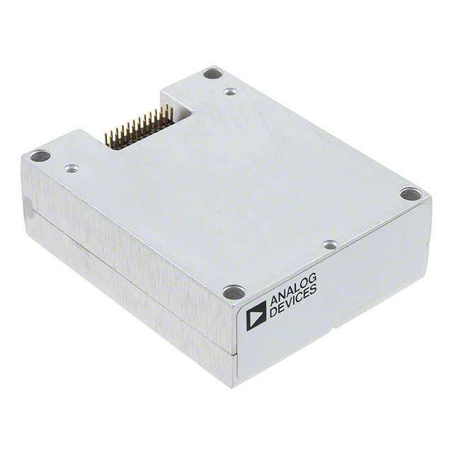
Data Sheet ADXRS450 ORDERING GUIDE Package Model1 Temperature Range Package Description Option ADXRS450BEYZ –40°C to +105°C 14-Terminal Ceramic Leadless Chip Carrier, Vertical Form [LCC_V] EY-14-1 ADXRS450BEYZ-RL –40°C to +105°C 14-Terminal Ceramic Leadless Chip Carrier, Vertical Form [LCC_V] EY-14-1 ADXRS450BRGZ –40°C to +105°C 16-Lead Small Outline, Plastic Cavity Package [SOIC_CAV] RG-16-1 ADXRS450BRGZ-RL –40°C to +105°C 16-Lead Small Outline, Plastic Cavity Package [SOIC_CAV] RG-16-1 EVAL-ADXRS450Z Evaluation Board SOIC_CAV EVAL-ADXRS450Z-V Evaluation Board LCC_V EVAL-ADXRS450Z-M Analog Devices Inertial Sensor Evaluation System (Includes ADXRS450 Satellite) EVAL-ADXRS450Z-S ADXRS450 Satellite, Standalone, to be used with Inertial Sensor Evaluation System 1 Z = RoHS Compliant Part. Rev. C | Page 27 of 28
ADXRS450 Data Sheet NOTES ©2011–2013 Analog Devices, Inc. All rights reserved. Trademarks and registered trademarks are the property of their respective owners. D08952-0-5/13(C) Rev. C | Page 28 of 28
Mouser Electronics Authorized Distributor Click to View Pricing, Inventory, Delivery & Lifecycle Information: A nalog Devices Inc.: EVAL-ADXRS450Z-V EVAL-ADXRS450Z ADXRS450BEYZ ADXRS450BRGZ EVAL-ADXRS450Z-S ADXRS450BEYZ-RL ADXRS450BRGZ-RL EVAL-ADXRS450Z-M