ICGOO在线商城 > 传感器,变送器 > 运动传感器 - 陀螺仪 > ADIS16060BCCZ
 Datasheet下载
- 型号: ADIS16060BCCZ
- 制造商: Analog
- 库位|库存: xxxx|xxxx
- 要求:
| 数量阶梯 | 香港交货 | 国内含税 |
| +xxxx | $xxxx | ¥xxxx |
查看当月历史价格
查看今年历史价格
ADIS16060BCCZ产品简介:
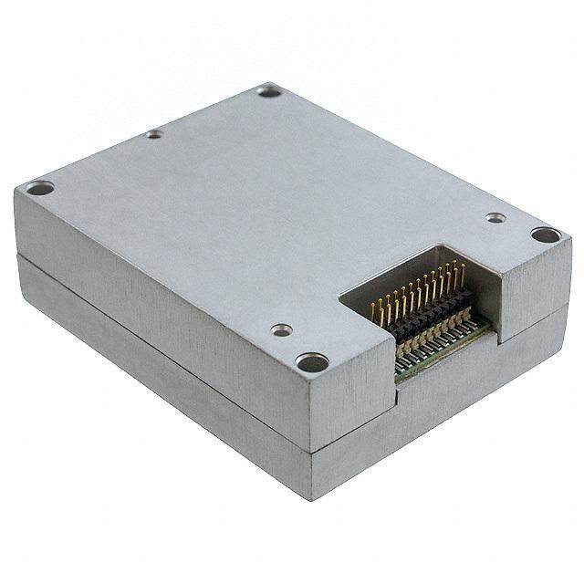
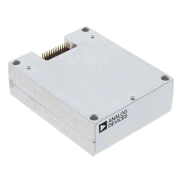
ICGOO电子元器件商城为您提供ADIS16060BCCZ由Analog设计生产,在icgoo商城现货销售,并且可以通过原厂、代理商等渠道进行代购。 ADIS16060BCCZ价格参考¥527.70-¥527.70。AnalogADIS16060BCCZ封装/规格:运动传感器 - 陀螺仪, Gyroscope Z (Yaw) ±80 1kHz SPI 16-LGA (8.2x8.2)。您可以下载ADIS16060BCCZ参考资料、Datasheet数据手册功能说明书,资料中有ADIS16060BCCZ 详细功能的应用电路图电压和使用方法及教程。
ADIS16060BCCZ 是 Analog Devices Inc.(ADI)生产的一款运动传感器 - 陀螺仪,属于 iSensor 系列。它是一款高性能、低噪声的单轴数字陀螺仪,集成了信号调理电路和数字接口,适用于需要高精度角速度测量的应用场景。以下是该型号的主要应用场景:

 1. 工业自动化与机器人
   - 在工业自动化领域,ADIS16060BCCZ 可用于机器人手臂的姿态控制和定位。通过精确测量旋转角度和角速度,确保机器人在复杂环境中实现精准的动作。
   - 应用于 CNC 机床、自动导引车(AGV)等设备中,提供稳定的方向感知和动态调整。

 2. 航空航天与导航
   - 该陀螺仪可作为惯性导航系统的一部分,用于飞行器、无人机或卫星的姿态控制。其高精度特性能够帮助保持稳定的飞行方向和姿态。
   - 在 GPS 信号弱或不可用的情况下,ADIS16060BCCZ 可提供可靠的惯性数据以辅助导航。

 3. 医疗设备
   - 在医疗领域,可用于手术机器人、康复设备或运动分析系统中。例如,监测患者的身体运动或协助医生进行精确的手术操作。
   - 提供高分辨率的角速度数据,支持实时反馈和调整。

 4. 振动监测与结构健康
   - 用于桥梁、建筑物或其他大型结构的振动监测。通过检测微小的旋转变化,评估结构的稳定性并预警潜在问题。
   - 在风力发电机中,可用于叶片的角度监测和优化运行效率。

 5. 消费电子与物联网
   - 虽然 ADIS16060BCCZ 主要面向工业级应用,但在高端消费电子产品中也可用于增强用户体验,如虚拟现实(VR)头盔的姿态跟踪或高端相机的防抖功能。
   - 在智能家居领域,可用于监控设备的运动状态,提高系统的智能化水平。

 特点总结
- 单轴角速度测量范围:±125°/s 或 ±300°/s。
- 内置温度补偿和自检功能,确保长期稳定性。
- SPI 数字接口,便于与微控制器或其他系统集成。

综上所述,ADIS16060BCCZ 的高精度和可靠性使其成为工业、航空、医疗等领域中关键任务的理想选择。
| 参数 | 数值 |
| 产品目录 | |
| 描述 | IC GYROSCOPE YAW RATE SPI 16LGA螺旋仪 Wide BW Yaw Rate w/ SPI |
| 产品分类 | 陀螺仪运动与定位传感器 |
| 品牌 | Analog Devices |
| 产品手册 | |
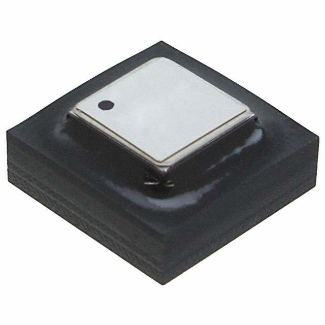
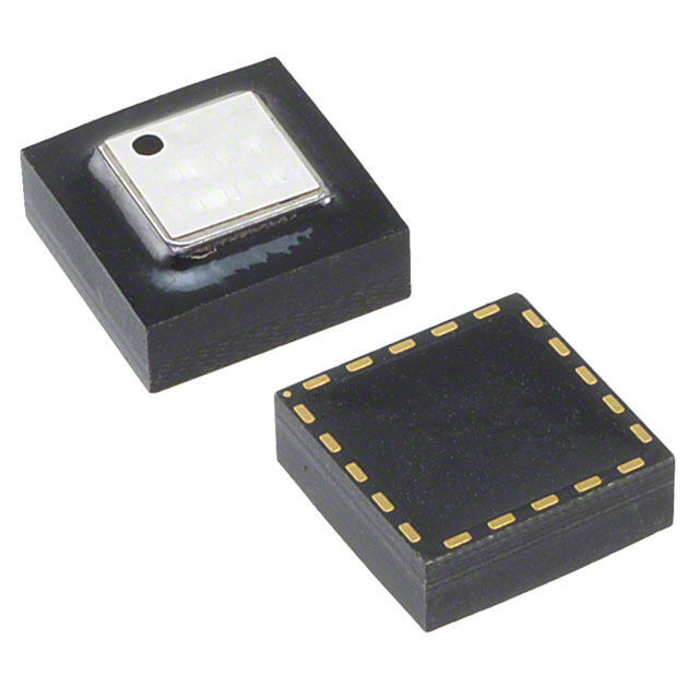
| 产品图片 |
|
| rohs | RoHS 合规性豁免无铅 / 符合限制有害物质指令(RoHS)规范要求 |
| 产品系列 | 螺旋仪,Analog Devices ADIS16060BCCZ- |
| 数据手册 | |
| 产品型号 | ADIS16060BCCZ |
| PCN设计/规格 | |
| 产品培训模块 | http://www.digikey.cn/PTM/IndividualPTM.page?site=cn&lang=zhs&ptm=38 |
| 产品目录页面 | |
| 产品种类 | 螺旋仪 |
| 传感轴 | Z |
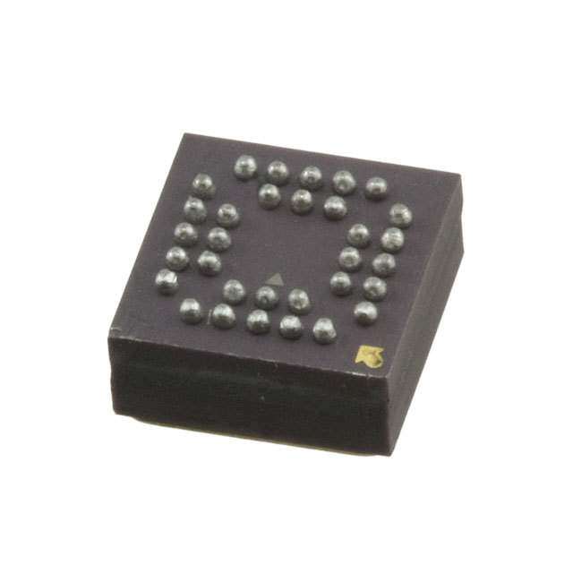
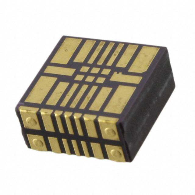
| 供应商器件封装 | 16-LGA(8.2x8.2) |
| 典型带宽 | 1kHz |
| 加速 | 2000 g |
| 商标 | Analog Devices |
| 宽度 | 8.2 mm |
| 封装 | Tray |
| 封装/外壳 | 16-BFLGA |
| 封装/箱体 | LGA-16 |
| 工作温度 | -40°C ~ 105°C |
| 工厂包装数量 | 260 |
| 带宽 | 1 kHz |
| 数字输出-位数 | 14 bit |
| 数字输出-总线接口 | SPI |
| 最大工作温度 | + 105 C |
| 最小工作温度 | - 40 C |
| 标准包装 | 1 |
| 灵敏度 | 0.0122 deg/s/LSB |
| 电压-电源 | 4.75 V ~ 5.25 V |
| 电流-电源 | 4.3mA |
| 电源电压-最大 | 5.25 V |
| 电源电压-最小 | 4.75 V |
| 电源电流 | 4.3 mA |
| 系列 | ADIS16060 |
| 范围 | +/- 80 deg/s |
| 范围°/s | ±80°/s |
| 输出类型 | Digital |
| 配用 | /product-detail/zh/ADIS16060%2FPCBZ/ADIS16060%2FPCBZ-ND/1771155 |
| 长度 | 8.2 mm |
| 高度 | 5.2 mm |


- 商务部:美国ITC正式对集成电路等产品启动337调查
- 曝三星4nm工艺存在良率问题 高通将骁龙8 Gen1或转产台积电
- 太阳诱电将投资9.5亿元在常州建新厂生产MLCC 预计2023年完工
- 英特尔发布欧洲新工厂建设计划 深化IDM 2.0 战略
- 台积电先进制程称霸业界 有大客户加持明年业绩稳了
- 达到5530亿美元!SIA预计今年全球半导体销售额将创下新高
- 英特尔拟将自动驾驶子公司Mobileye上市 估值或超500亿美元
- 三星加码芯片和SET,合并消费电子和移动部门,撤换高东真等 CEO
- 三星电子宣布重大人事变动 还合并消费电子和移动部门
- 海关总署:前11个月进口集成电路产品价值2.52万亿元 增长14.8%

PDF Datasheet 数据手册内容提取
Wide Bandwidth Yaw Rate Gyroscope with SPI Data Sheet ADIS16060 FEATURES GENERAL DESCRIPTION Complete angular rate digital gyroscope The ADIS16060 is a yaw rate gyroscope with an integrated 14-bit resolution serial peripheral interface (SPI). It features an externally Scalable measurement range selectable bandwidth response and scalable dynamic range. Initial range: ±80°/sec (typical) The SPI port provides access to the rate sensor, an internal Increase range with external resistor temperature sensor, and two external analog signals (using Z-axis (yaw rate) response internal ADC). The digital data available at the SPI port is SPI digital output interface proportional to the angular rate about the axis that is normal High vibration rejection over wide frequency to the top surface of the package. 2000 g-powered shock survivability 1 kHz bandwidth An additional output pin provides a precision voltage reference. Selectable using external capacitor A digital self-test function electromechanically excites the sensor Externally controlled self-test to test the operation of the sensor and the signal-conditioning Internal temperature sensor output circuits. Dual auxiliary 14-bit ADC inputs The ADIS16060 is available in an 8.2 mm × 8.2 mm × 5.2 mm, Absolute rate output for precision applications 16-terminal, peripheral land grid array (LGA) package. 5 V single-supply operation 8.2 mm × 8.2 mm × 5.2 mm package −40°C to +105°C operation RoHS compliant APPLICATIONS Platform stabilization Image stabilization Guidance and control Inertial measurement units Robotics FUNCTIONAL BLOCK DIAGRAM FILT RATE VCC ADIS16060 RATE SENSOR SCLK 14-BIT DIN TEMPERATURE MUX ADC DOUT SENSOR DIGITAL MSEL1 CONTROL MSEL2 AIN1 AIN2 GND 07103-001 Figure 1. Rev. A Information furnished by Analog Devices is believed to be accurate and reliable. However, no responsibility is assumed by Analog Devices for its use, nor for any infringements of patents or other One Technology Way, P.O. Box 9106, Norwood, MA 02062-9106, U.S.A. rights of third parties that may result from its use. Specifications subject to change without notice. No license is granted by implication or otherwise under any patent or patent rights of Analog Devices. Tel: 781.329.4700 www.analog.com Trademarks and registered trademarks are the property of their respective owners. Fax: 781.461.3113 ©2008–2012 Analog Devices, Inc. All rights reserved.
ADIS16060 Data Sheet TABLE OF CONTENTS Features .............................................................................................. 1 Basic Operation .............................................................................. 10 Applications ....................................................................................... 1 Serial Peripheral Interface (SPI) ............................................... 10 General Description ......................................................................... 1 Output Data Formatting ............................................................ 10 Functional Block Diagram .............................................................. 1 ADC Conversion ........................................................................ 10 Revision History ............................................................................... 2 Applications Information .............................................................. 11 Specifications ..................................................................................... 3 Supply And Common Considerations .................................... 11 Timing Specifications .................................................................. 5 Setting Bandwidth ...................................................................... 11 Absolute Maximum Ratings ............................................................ 6 Increasing Measurement Range ............................................... 11 ESD Caution .................................................................................. 6 Dynamic Digital Sensitivity Scaling ........................................ 11 Pin Configuration and Function Descriptions ............................. 7 Temperature Measurements ..................................................... 11 Typical Performance Characteristics ............................................. 8 Self-Test Function ...................................................................... 11 Theory of Operation ........................................................................ 9 Outline Dimensions ....................................................................... 12 Analog-to-Digital Converter Input ............................................ 9 Ordering Guide .......................................................................... 12 Rate Sensitive Axis ....................................................................... 9 REVISION HISTORY 4/12—Rev. 0 to Rev. A Updated Format .................................................................. Universal Changes to Applications Section .................................................... 1 Changes to Note 1 in Figure 4 ......................................................... 7 Changes to Supply and Common Considerations Section, Setting Bandwidth Section, and Figure 14 Caption ................... 11 1/08—Revision 0: Initial Version Rev. A | Page 2 of 12
Data Sheet ADIS16060 SPECIFICATIONS T = 25°C, V = 5 V, angular rate = 0°/sec, C = 0.01 μF, ±1 g, unless otherwise noted. A CC OUT Table 1. Parameter Test Conditions/Comments Min1 Typ Max Unit SENSITIVITY Dynamic Range2 Full-scale range over specifications range ±50 ±80 °/sec Initial Clockwise rotation is positive output, 0.0110 0.0122 0.0134 °/sec/LSB T = −40°C to +85°C A Change Over Temperature3 V = 4.75 V to 5.25 V ±3 % CC Nonlinearity Best fit straight line 0.1 °/sec NULL Initial Nominal 0°/sec output is 8192 LSB −44 +44 °/sec Change Over Temperature3 V = 4.75 V to 5.25 V ±0.11 °/sec/°C CC Turn-On Time Power on to ±0.5°/sec of final value 10 ms Linear Acceleration Effect Any axis ±0.1 °/sec/g Voltage Sensitivity V = 4.75 V to 5.25 V ±0.5 °/sec/V CC NOISE PERFORMANCE Rate Noise Density @ 25°C 0.04 °/sec/√Hz FREQUENCY RESPONSE 3 dB Bandwidth (User-Selectable)4 C = 0 µF 1 1000 Hz OUT Sensor Resonant Frequency 14.5 kHz SELF-TEST RESPONSE Positive Self-Test5 See Table 5 +6226 LSB Negative Self-Test5 See Table 5 −6226 LSB TEMPERATURE SENSOR Reading at 298 K 7700 8192 8684 LSB Scale Factor Proportional to absolute temperature 0.034 K/LSB LOGIC INPUTS Input High Voltage, V 0.7 × V V INH CC Input Low Voltage, V 0.8 V INL Input Current, I Typically 10 nA −1 +1 µA IN Input Capacitance, C (DIN) 8 pF IN Input Capacitance, CIN (MSEL1, MSEL2) 5 pF ANALOG INPUTS For V < V IN CC Resolution 14 Bits Integral Nonlinearity Best fit straight line −6 +6 LSB Differential Nonlinearity No missing codes to 13 bits −1 +6 LSB Offset Error −10 +10 mV Offset Error Temperature Drift ±0.3 ppm/°C Gain Error −40 +40 mV Gain Error Temperature Drift ±0.3 ppm/°C Input Voltage Range 0 V V CC Leakage Current 1 nA DIGITAL OUTPUTS Output High Voltage, V I = 500 µA V − 0.3 V OH SOURCE CC Output Low Voltage, V I = 500 µA 0.4 V OL SINK CONVERSION RATE Conversion Time 10 µs Throughput Rate 100 kSPS Rev. A | Page 3 of 12
ADIS16060 Data Sheet Parameter Test Conditions/Comments Min1 Typ Max Unit POWER SUPPLY All at T = −40°C to +85°C A V 4.75 5 5.25 V CC V Quiescent Supply Current V @ 5 V, 50 kSPS sample rate 4.3 6.5 mA CC CC Power Dissipation V @ 5 V, 50 kSPS sample rate 22 33 mW CC TEMPERATURE RANGE Operation −40 +105 °C 1 All minimum and maximum specifications are guaranteed. Typical specifications are neither tested nor guaranteed. 2 Dynamic range is the maximum full-scale measurement range possible, including output swing range, initial offset, sensitivity, offset drift, and sensitivity drift at 5 V supply. 3 Defined as the output change from ambient to maximum temperature, or ambient to minimum temperature. 4 Frequency at which the response is 3 dB down from dc response. Bandwidth = 1/(2 × π × 200 kΩ × COUT). For COUT = 0.01 μF, bandwidth = 80 Hz. 5 Self-test response varies with temperature. Rev. A | Page 4 of 12
Data Sheet ADIS16060 TIMING SPECIFICATIONS T = 25°C, angular rate = 0°/sec, unless otherwise noted.1 A Table 2. Read/Output Sequence Parameter Figure Reference Symbol Min Typ Max Unit Serial Clock Frequency 2.9 MHz Throughput Rate See Figure 2 t 100 kHz CYC MSEL1 Falling to SCLK Low See Figure 2 t 0 μs CSD MSEL1 Falling to SCLK Rising See Figure 2 t 20 ns SUCS SLCK Falling to Data Remains Valid See Figure 2 t 5 16 ns HDO MSEL1 Rising Edge to D High Impedance See Figure 2 t 14 100 ns OUT DIS SCLK Falling to Data Valid See Figure 2 t 16 50 ns EN Acquisition Time See Figure 2 t 400 ns ACQ D Fall Time See Figure 2 t 11 25 ns OUT F D Rise Time See Figure 2 t 11 25 ns OUT R Data Setup Time See Figure 3 t 5 5 ns 5 SCLK Falling Edge to MSEL2 Rising Edge See Figure 3 t 0 0 ns 7 Data Hold Time See Figure 3 t 4.5 ns 6 1 Guaranteed by design. All input signals are specified with tR = tF = 5 ns (10% to 90% of VCC) and timed from a voltage level of 1.6 V. The 5 V operating range spans from 4.75 V to 5.25 V. Timing Diagrams tCYC COMPLETE CYCLE MSEL1 tSUCS tACQ POWERDOWN SCLK 1 4 5 tCSD tEN tHDO tDIS HIGH-Z HIGH-Z DOUT 0 D13 D12 D11 D10 D9 D8 D7 D6 D5 D4 D3 D2 D1 D0 0 NA OMTINE:IMUM OF 20 CLOCK CYCLES (AMRSEB )REQUIRED FOR 14-BIT CONVERSION. (LSB) 07103-002 Figure 2. Serial Interface Timing Diagram—Read/Output Sequence (CPOL = 0, CPHA = 0) t7 MSEL2 t5 t6 SCLK DIN DB7 DB6 DB5 DB4 DB3 DB2 DB1 DB0 NTHOET EL:AST EIGHT BITS CLOCKED IN ARE LATCHED WITH THE RISING EDGE OF THE MSEL2 LINE. 07103-003 Figure 3. Serial Interface Timing—Input/Configuration Sequence (CPOL = 0, CPHA = 1) Rev. A | Page 5 of 12
ADIS16060 Data Sheet ABSOLUTE MAXIMUM RATINGS Stresses above those listed under Absolute Maximum Ratings Table 3. may cause permanent damage to the device. This is a stress Parameter Rating rating only; functional operation of the device at these or any Acceleration (Any Axis, Unpowered, 0.5 ms) 2000 g other conditions above those indicated in the operational Acceleration (Any Axis, Powered, 0.5 ms) 2000 g section of this specification is not implied. Exposure to absolute V to GND −0.3 V to +6.0 V CC maximum rating conditions for extended periods may affect V to GND −0.3 V to V + 0.3 V CC CC device reliability. Analog Input Voltage to GND −0.3 V to V + 0.3 V CC Drops onto hard surfaces can cause shocks of greater than Digital Input Voltage to GND −0.3 V to +7.0 V 2000 g and exceed the absolute maximum rating of the device. Digital Output Voltage to GND −0.3 V to V + 0.3 V CC Care should be exercised in handling the device to avoid damage. Operating Temperature Range −40°C to +105°C Storage Temperature Range −65°C to +150°C ESD CAUTION Rev. A | Page 6 of 12
Data Sheet ADIS16060 PIN CONFIGURATION AND FUNCTION DESCRIPTIONS 1 2 L L MSE MSE VCC GND 16 15 14 13 DIN 1 12 GND 3.68685×BSC PIN1 2.5050BSC INDICATOR 8× SCLK 2 ADIS16060 11 GND 0.6700BSC TOP 12× “LOOKTHROUGH” DOUT 3 VIEW 10 GND (NottoScale) NC 4 9 AIN2 7.373BSC 5.010BSC 2× 4× 5 6 7 8 E T C 1 RAT FIL VC AIN NOTES 1. PINS LABELED NC CAN BE ALLOWED TO FLOAT, BUT IT IS BETTER TO CONNECT THESE PINS TO GROUND. AVOID ROUTING HIGH SPEED SIGNALS THROUGH THESE PINS BACAUSE NOISE COUPLING MAY RESULT. 2. TTPTOHHREIOPS .VP ITISADH CENISKDO A ITFSG O AAERN LI SPAA CCLYBTOO UOLUAAKTLY EV O“DITE UTOWTHP ,RP WVUOIHREUIPWGCOHH,”S FRAERESSOP. TRMHE ETS HPEEINN TTSSO A PTR.H ETEH NPISOIN TC COVOINSNFIBFIGILGUEUR FRARATOTIOMION TN IH,S EIF 07103-004 1.000B1S6C× 0.5000B1S6C× 07103-005 Figure 4. Pin Configuration Figure 5. Second-Level Assembly Pad Layout Table 4. Pin Function Descriptions Pin No. Mnemonic Type1 Description 1 DIN I SPI Data Input. 2 SCLK I SPI Serial Clock. 3 DOUT O SPI Data Output. 4 NC This pin is not connected internally (see Figure 4). 5 RATE O Buffered Analog Output. Represents the angular rate signal. 6 FILT I External Capacitor Connection to Control Bandwidth. 7 V S Power Supply. CC 8 AIN1 I External Analog Input Channel 1. 9 AIN2 I External Analog Input Channel 2. 10 GND S Ground. 11 GND S Ground. 12 GND S Ground. 13 GND S Ground. 14 V S Power Supply. CC 15 MSEL2 I SPI, Mode Select 2. User for data input functions. 16 MSEL1 I SPI, Mode Select 1. Used for data output functions. 1 I = input; O = output; S = power supply. Rev. A | Page 7 of 12
ADIS16060 Data Sheet TYPICAL PERFORMANCE CHARACTERISTICS 0.18 6800 B)6600 0.16 S L TION (%) 00..1124 SPONSE (66420000 LA RE6000 PU 0.10 UT O P5800 P T OF 0.08 OU5600 T E EN 0.06 AT5400 C R R L PE 0.04 TA5200 GI 0.02 DI5000 0 –44–40–36–32–28–24–20–16–12–8BIA–4S 0(°/s4ec8) 121620242832364044 07103-020 4800–60 –40 –20 0TEMP2E0RATU4R0E(°C6)0 80 100 120 07103-009 Figure 6. Initial Bias Error Distribution, 25°C, VCC = 5 V Figure 9. Positive Self-Test Response vs. Temperature, VCC = 5 V 0.30 –4800 B)–5000 S 0.25 L %) E (–5200 ( S N N O O–5400 ATI 0.20 SP UL RE–5600 P T PO 0.15 PU–5800 ERCENTOF 0.10 L RATE OUT––66020000 P 0.05 TA–6400 GI DI–6600 0 –0.60–0.55–0.50–0.45BI–0.40AS–0.35D–0.30RI–0.25FT–0.20O–0.15VE–0.10RT–0.05E0MP0.05ER0.10A0.15TU0.20RE0.25(°0.30/se0.35c/0.40°C)0.450.500.550.60 07103-021 –6800–60 –40 –20 0TEMP2E0RATU4R0E (°C)60 80 100 120 07103-010 Figure 7. Bias Drift Over −40°C to +85°C, VCC = 5 V Figure 10. Negative Self-Test Output Response vs. Temperature, VCC = 5 V 0.04 0.1 0.03 c) ERROR (%) 00..0021 µ + 1σ RIANCE (°/se VITY 0 µ N VA 0.01 SITI–0.01 LLE N A SE–0.02 OT O R µ – 1σ –0.03 –0.04 0.001 –60 –40 –20 0TEMP2E0RATU2R0E (°C6)0 80 100 120 07103-008 1 10 Tau(°C) 100 1000 07103-011 Figure 8. Sensitivity Drift vs. Temperature, VCC = 5 V Figure 11. Allen Variance, 25°C, VCC = 5 V Rev. A | Page 8 of 12
Data Sheet ADIS16060 THEORY OF OPERATION The ADIS16060 operates on the principle of a resonator During the acquisition phase, the impedance model for AINx gyroscope. Two polysilicon sensing structures each contain a is a parallel combination of the capacitor C and the network PIN dither frame that is electrostatically driven to resonance. This formed by the series connection of R and C . C is primarily IN IN PIN generates the necessary velocity element to produce a Coriolis the pin capacitance. R is typically 600 Ω and is a lumped IN force while rotating. At two of the outer extremes of each frame, component made up of some serial resistors and the on orthogonal to the dither motion, are movable fingers that are resistance of the switches. C is typically 30 pF and mainly IN placed between fixed pickoff fingers to form a capacitive pickoff functions as the ADC sampling capacitor. structure that senses Coriolis motion. During the conversion phase, when the switches are open, the The resulting signal is fed to a series of gain and demodulation input impedance is limited to C . R and C make a 1-pole, PIN IN IN stages that produce the electrical rate signal output. The rate low-pass filter that reduces undesirable aliasing effects and signal is then converted to a digital representation of the limits the noise. output on the SPI pins. The dual-sensor design provides When the source impedance of the driving circuit is low, the linear acceleration (vibration, shock) rejection. Fabricating ADC input can be driven directly. Large source impedances the sensor with the signal-conditioning electronics preserves significantly affect the ac performance, especially THD. The signal integrity in noisy environments. dc performances are less sensitive to the input impedance. The electrostatic resonator requires 14 V to 16 V for operation. RATE SENSITIVE AXIS Because only 5 V is typically available in most applications, a RATE charge pump is included on chip. After the demodulation stage, AXIS a single-pole, low-pass filter on the chip is used to limit high LONGITUDINAL AXIS POSITIVE frequency artifacts before final amplification. The frequency MEASUREMENT DIRECTION response is dominated by the second low-pass filter, which is 8 set by adding capacitance across RATE and FILT. ANALOG-TO-DIGITAL CONVERTER INPUT 1LAATXEIRSAL4 5 07103-019 Figure 12 shows an equivalent circuit of the input structure of Figure 13. Rate Signal Increases with Clockwise Rotation the ADIS16060 auxiliary ADC. The two diodes, D1 and D2, provide ESD protection for the analog inputs, AINx (AIN1 and AIN2). Care must be taken to ensure that the analog input signal does not exceed the supply rails by more than 0.3 V, because exceeding this level causes these diodes to become forward-biased and to start conducting current. However, these diodes can handle a forward-biased current of 130 mA maximum. For instance, these conditions may eventually occur when the input signals exceed either VCC or GND. VDD D1 RIN CIN AINx CPIN D2 GND 07103-018 Figure 12. Equivalent Analog Input Circuit Rev. A | Page 9 of 12
ADIS16060 Data Sheet BASIC OPERATION The ADIS16060 is designed for simple integration into indus- Output Data Access trial system designs, requiring only a 5 V power supply, two Use Table 2 and Figure 2 to determine the appropriate timing mode select lines, and three serial communications lines. The considerations for reading output data. SPI handles all digital I/O communication in the ADIS16060. OUTPUT DATA FORMATTING SERIAL PERIPHERAL INTERFACE (SPI) All of the output data is in an offset-binary format, which in The ADIS16060 SPI port includes five signals: Mode Select 1 this case, means that the ideal output for a zero rate condition is (MSEL1), Mode Select 2 (MSEL2), serial clock (SCLK), data 8192 codes. If the sensitivity is equal to +0.0122°/sec/LSB, a rate input (DIN), and data output (DOUT). The MSEL1 line is used of +10°/sec results in a change of 820 codes, and a digital rate when reading data out of the sensor (DOUT), and the MSEL2 output of 9012 codes. If an offset error of −20°/sec is introduced, line is used when configuring the sensor (DIN). the output is reduced by 1639 codes (if typical sensitivity is Selecting Output Data assumed), resulting in a digital rate output of 6552 codes. ADC CONVERSION Refer to Table 5 to determine the appropriate DIN bit sequence based on the required data source. Table 2 and Table 3 provide The internal successive approximation ADC begins the the necessary timing details for the input configuration sequence. conversion process on the falling edge of MSEL1 and starts to After the MSEL2 goes high, the last eight DIN bits are loaded place data MSB first on the DOUT line at the 6th falling edge of into the internal control register, which represents DB0 to DB7 SCLK, as shown in Figure 2. The entire conversion process in Table 5. takes 20 SCLK cycles. After MSEL1 goes high, the acquisition process starts in preparation for the next conversion cycle. Table 5. DIN Configuration Bit Assignments Action DB7 DB6 DB5 DB4 DB3 DB2 DB1 DB0 Measure Angular Rate (Gyro) 0 0 1 0 0 0 0 0 Measure Temperature 0 0 0 1 0 0 0 0 Measure AIN2 1 0 0 0 0 0 0 0 Measure AIN1 0 1 0 0 0 0 0 0 Set Positive Self-Test and Output for Angular Rate 0 0 1 0 0 0 1 0 Set Negative Self-Test and Output for Angular Rate 0 0 1 0 0 0 0 1 Rev. A | Page 10 of 12
Data Sheet ADIS16060 APPLICATIONS INFORMATION SUPPLY AND COMMON CONSIDERATIONS 1 Power supply noise and transient behaviors can influence the accuracy and stability of any sensor-based measurement Hz) 0.1 system. Power supply stability and source impedance can √ c/ e influence performance. While the ADIS16060 provides 0.2 µF s of capacitance on the VCC pin, additional capacitors will support SITY (°/ 0.01 optimum performance. N E D SETTING BANDWIDTH E S OI N0.001 External Capacitor C is used in combination with the OUT on-chip R resistor to create a low-pass filter to limit the OUT bandwidth of the ADIS16060 rate response. The –3 dB 0.0001 frequency set by ROUT a1nd COUT is 10 100 FREQUE1NkCY (Hz) 10k 100k 07103-118 f = Figure 14. Spectral Noise Density, fs = 50 kHz, 80 Hz, Single-Pole Filter OUT (2×π×R ×C ) OUT OUT DYNAMIC DIGITAL SENSITIVITY SCALING and can be well controlled because R has been trimmed OUT This device supports in-system, dynamic, digital sensitivity during manufacturing to be 200 kΩ ± 5%. Setting the range scaling. with an external resistor impacts R as follows: OUT ( ) TEMPERATURE MEASUREMENTS 200kΩ×R R = EXT OUT (200kΩ+R ) When using the temperature sensor, an acquisition time of EXT greater than 40 μs helps to ensure proper setting and measurement In general, additional filter poles (analog or digital) can accuracy. See Table 2 and Figure 2 for details on the definition contribute to reducing the noise associated with the of acquisition time. demodulation spikes (~14 kHz) in Figure 14. SELF-TEST FUNCTION INCREASING MEASUREMENT RANGE Exercising the self-test function is simple, as shown in this Scaling the measurement range requires the addition of a single example. resistor, connected across the RATE and FILT pins. The 1. Configure using DIN = 00100010 (positive self-test, rate following equation provides the proper relationship for selected). selecting the appropriate resistor: 2. Read output. 200kΩ 3. Configure using DIN = 00100000 (positive self-test off, rate R = EXT ∆−1 selected). 4. Read output. where Δ is the increase in range. 5. Calculate the difference between Step 2 and Step 4, and compare this with the specified self-test output changes in the Specifications section. Exercising the negative self-test requires changing the sequence in Step 1 to DIN = 00100001. Rev. A | Page 11 of 12
ADIS16060 Data Sheet OUTLINE DIMENSIONS 5.010 BSC 2.505 (4×) PIN 1 BSC INDICATOR 8.35 (8×) MAX 0.873 BSC (16×) 13 16 12 1 7.373 8.20 BSC TYP (2×) 0.797 BSC (12×) 9 4 8 5 TOP VIEW 0.200 BOTTOM VIEW 0.373 BSC MIN (16×) (ALL SIDES) 7.00 TYP 5.20 MAX SIDE VIEW 022107-B Figure 15. 16-Terminal Stacked Land Grid Array [LGA] (CC-16-1) Dimensions shown in millimeters ORDERING GUIDE Model1 Temperature Range Package Description Package Option ADIS16060BCCZ −40°C to +105°C 16-Terminal Stacked Land Grid Array (LGA) CC-16-1 ADIS16060/PCBZ Evaluation Board 1 Z = RoHS Compliant Part. ©2008–2012 Analog Devices, Inc. All rights reserved. Trademarks and registered trademarks are the property of their respective owners. D07103-0-4/12(A) Rev. A | Page 12 of 12