ICGOO在线商城 > 传感器,变送器 > 运动传感器 - 陀螺仪 > ADXRS646BBGZ
 Datasheet下载
- 型号: ADXRS646BBGZ
- 制造商: Analog
- 库位|库存: xxxx|xxxx
- 要求:
| 数量阶梯 | 香港交货 | 国内含税 |
| +xxxx | $xxxx | ¥xxxx |
查看当月历史价格
查看今年历史价格
ADXRS646BBGZ产品简介:
ICGOO电子元器件商城为您提供ADXRS646BBGZ由Analog设计生产,在icgoo商城现货销售,并且可以通过原厂、代理商等渠道进行代购。 ADXRS646BBGZ价格参考¥889.10-¥889.10。AnalogADXRS646BBGZ封装/规格:运动传感器 - 陀螺仪, Gyroscope Z (Yaw) ±250 1kHz Analog Voltage 32-CBGA (7x7)。您可以下载ADXRS646BBGZ参考资料、Datasheet数据手册功能说明书,资料中有ADXRS646BBGZ 详细功能的应用电路图电压和使用方法及教程。
ADXRS646BBGZ 是由 Analog Devices Inc.(ADI)生产的一款运动传感器,属于陀螺仪类别。该型号的陀螺仪具有高精度、低漂移和宽测量范围的特点,适合多种应用场景。以下是其主要的应用场景:

1. 惯性导航系统:ADXRS646BBGZ 可用于航空、航海和陆地车辆的惯性导航系统中,提供精确的角速度测量数据,帮助设备确定方向和位置。

2. 稳定控制系统:在无人机、相机云台或卫星天线等需要高稳定性的设备中,该陀螺仪可用于检测和校正旋转运动,确保设备保持稳定。

3. 机器人技术:在工业机器人和服务机器人中,ADXRS646BBGZ 可以帮助检测机器人的姿态和运动状态,从而实现更精确的控制和操作。

4. 振动监测与分析:该陀螺仪可用于工业设备的振动监测,通过检测旋转运动的变化来识别潜在故障或异常情况。

5. 医疗设备:在某些医疗设备中,如康复训练设备或手术机器人,ADXRS646BBGZ 可以提供精确的姿态信息,支持设备的平稳运行。

6. 汽车电子:在汽车电子稳定程序(ESP)或防侧翻系统中,该陀螺仪可以检测车辆的倾斜角度和旋转速度,提高行车安全性。

7. 消费电子产品:例如游戏控制器或虚拟现实(VR)设备,ADXRS646BBGZ 能够捕捉用户的手部动作或头部转动,增强交互体验。

总之,ADXRS646BBGZ 凭借其高性能和可靠性,广泛应用于需要精确角度测量和运动控制的领域,为各种设备提供关键的传感技术支持。
| 参数 | 数值 |
| 产品目录 | |
| 描述 | IC GYROSCOPE YAW RATE 32CBGA螺旋仪 Vibration Reject Hi Stabilty Yaw Rate |
| 产品分类 | 陀螺仪运动与定位传感器 |
| 品牌 | Analog Devices Inc |
| 产品手册 | |
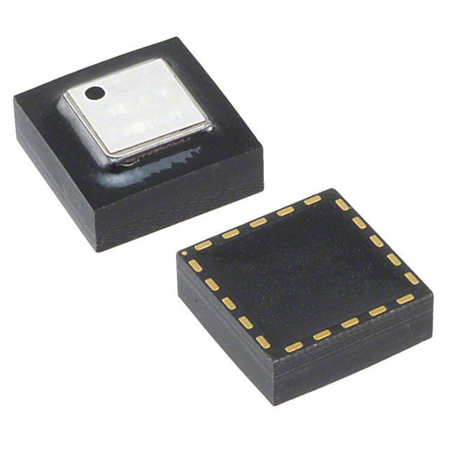
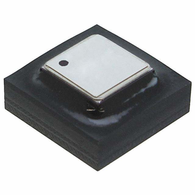
| 产品图片 |
|
| rohs | RoHS 合规性豁免无铅 / 符合限制有害物质指令(RoHS)规范要求 |
| 产品系列 | 螺旋仪,Analog Devices ADXRS646BBGZ- |
| 数据手册 | |
| 产品型号 | ADXRS646BBGZ |
| PCN组件/产地 | |
| PCN设计/规格 | |
| 产品种类 | 螺旋仪 |
| 传感轴 | Z |
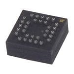
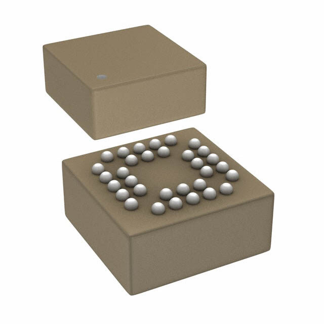
| 供应商器件封装 | 32-CBGA(7x7) |
| 其它名称 | Q6420350 |
| 典型带宽 | 1kHz |
| 加速 | 10000 g |
| 商标 | Analog Devices |
| 宽度 | 7 mm |
| 封装 | Bulk |
| 封装/外壳 | 32-BFCBGA |
| 封装/箱体 | CBGA-32 |
| 工作温度 | -40°C ~ 105°C |
| 工厂包装数量 | 20 |
| 带宽 | 1000 Hz |
| 数字输出-位数 | - |
| 数字输出-总线接口 | - |
| 最大工作温度 | + 105 C |
| 最小工作温度 | - 40 C |
| 标准包装 | 1 |
| 灵敏度 | 9mV/°/s |
| 电压-电源 | 5.75 V ~ 6.25 V |
| 电流-电源 | 4mA |
| 电源电压-最大 | 6.25 V |
| 电源电压-最小 | 5.75 V |
| 电源电流 | 4 mA |
| 系列 | ADXRS646 |
| 范围 | +/- 250 deg/s |
| 范围°/s | ±300°/s |
| 输出类型 | 模拟 |
| 长度 | 7 mm |
| 高度 | 3 mm |


- 商务部:美国ITC正式对集成电路等产品启动337调查
- 曝三星4nm工艺存在良率问题 高通将骁龙8 Gen1或转产台积电
- 太阳诱电将投资9.5亿元在常州建新厂生产MLCC 预计2023年完工
- 英特尔发布欧洲新工厂建设计划 深化IDM 2.0 战略
- 台积电先进制程称霸业界 有大客户加持明年业绩稳了
- 达到5530亿美元!SIA预计今年全球半导体销售额将创下新高
- 英特尔拟将自动驾驶子公司Mobileye上市 估值或超500亿美元
- 三星加码芯片和SET,合并消费电子和移动部门,撤换高东真等 CEO
- 三星电子宣布重大人事变动 还合并消费电子和移动部门
- 海关总署:前11个月进口集成电路产品价值2.52万亿元 增长14.8%
PDF Datasheet 数据手册内容提取
High Stability, Low Noise Vibration Rejecting Yaw Rate Gyroscope Data Sheet ADXRS646 FEATURES GENERAL DESCRIPTION 12°/hr bias stability The ADXRS646 is a high performance angular rate sensor Z-axis (yaw rate) response (gyroscope) that offers excellent vibration immunity. Bias 0.01°/√sec angle random walk stability is a widely-recognized figure of merit for high High vibration rejection over wide frequency performance gyroscopes, but in real-world applications, Measurement range extendable to a maximum of ±450°/sec vibration sensitivity is often a more significant performance 10,000 g powered shock survivability limitation and should be considered in gyroscope selection. The Ratiometric to referenced supply ADXRS646 offers superior vibration immunity and acceleration 6 V single-supply operation rejection as well as a low bias drift of 12°/hr (typical), enabling it −40°C to +105°C operation to offer rate sensing in harsh environments where shock and Self-test on digital command vibration are present. Ultrasmall and light (<0.15 cc, <0.5 gram) The ADXRS646 is manufactured using the Analog Devices, Temperature sensor output Inc., patented high volume BiMOS surface-micromachining Complete rate gyroscope on a single chip process. An advanced, differential, quad sensor design provides RoHS compliant the improved acceleration and vibration rejection. The output APPLICATIONS signal, RATEOUT, is a voltage proportional to angular rate about the axis normal to the top surface of the package. The Industrial applications measurement range is a minimum of ±250°/sec. The output is Severe mechanical environments ratiometric with respect to a provided reference supply. Other Platform stabilization external capacitors are required for operation. A temperature output is provided for compensation techniques. Two digital self-test inputs electromechanically excite the sensor to test proper operation of both the sensor and the signal condi- tioning circuits. The ADXRS646 is available in a 7 mm × 7 mm × 3 mm CBGA chip-scale package. FUNCTIONAL BLOCK DIAGRAM 3VTO 6V (ADC REF) 100nF 6V AVCC ST2 ST1 TEMP VRATIO ADXRS646 100nF SELF-TEST 25kΩ 25kΩ @ 25°C AGND DEMOD DARMIVPE MESCEHNASNOICRAL AAMCP VGA 6V ROUT VDD CHARGE PUMP 180kΩ ±1% AND VOLTAGE 100nF REGULATOR PGND CP1 CP2 CP3 CP4 CP5 SUMJ RATEOUT 22nF 22nF 100nF COUT 09771-001 Figure 1. Rev. C Document Feedback Information furnished by Analog Devices is believed to be accurate and reliable. However, no responsibility is assumed by Analog Devices for its use, nor for any infringements of patents or other One Technology Way, P.O. Box 9106, Norwood, MA 02062-9106, U.S.A. rights of third parties that may result from its use. Specifications subject to change without notice. No license is granted by implication or otherwise under any patent or patent rights of Analog Devices. Tel: 781.329.4700 ©2011–2017 Analog Devices, Inc. All rights reserved. Trademarks and registered trademarks are the property of their respective owners. Technical Support www.analog.com
ADXRS646 Data Sheet TABLE OF CONTENTS Features .............................................................................................. 1 Theory of Operation .........................................................................9 Applications ....................................................................................... 1 Setting Bandwidth .........................................................................9 General Description ......................................................................... 1 Temperature Output and Calibration .........................................9 Functional Block Diagram .............................................................. 1 Supply Ratiometricity ................................................................ 10 Revision History ............................................................................... 2 Null Adjustment ......................................................................... 10 Specifications ..................................................................................... 3 Self-Test Function ...................................................................... 10 Absolute Maximum Ratings ............................................................ 4 Continuous Self-Test .................................................................. 10 Rate Sensitive Axis ....................................................................... 4 Modifying the Measurement Range ........................................ 10 ESD Caution .................................................................................. 4 Immunity to Vibration .............................................................. 11 Pin Configuration and Function Descriptions ............................. 5 Outline Dimensions ....................................................................... 12 Typical Performance Characteristics ............................................. 6 Ordering Guide .......................................................................... 12 REVISION HISTORY 1/2017—Rev. B to Rev. C 9/2012—Rev. 0 to Rev. A Changes to Initial Parameter, Table 1 ............................................ 3 Changes to Figure 1 ........................................................................... 1 Changes to Figure 9 ........................................................................... 6 1/2014—Rev. A to Rev. B Changes to Table 1 ............................................................................ 3 9/2011—Revision 0: Initial Version Changes to Figure Captions, Typical Performance Characteristics Section ..................................................................... 6 Replaced Figure 8 ............................................................................. 6 Changes to Continuous Self-Test Section ................................... 10 Rev. C | Page 2 of 12
Data Sheet ADXRS646 SPECIFICATIONS All minimum and maximum specifications are guaranteed. Typical specifications are not guaranteed. T = 25°C, V = AV = V = 6 V, V = AV , angular rate = 0°/sec, bandwidth = 80 Hz (C = 0.01 µF), I = 100 µA, ±1 g, unless A S CC DD RATIO CC OUT OUT otherwise noted. Table 1. Parameter Test Conditions/Comments Min Typ Max Unit SENSITIVITY1 Clockwise rotation is positive output Measurement Range2 Full-scale range over specifications range ±250 ±300 °/sec Initial 7.5 9 10.5 mV/°/sec Temperature Drift3 ±6.5 % Nonlinearity Best fit straight line 0.01 % of FS NULL1 Null −40°C to +105°C 2.7 3.0 3.3 V Temperature Drift3 ±3 °/sec Linear Acceleration Effect Any axis 0.015 °/sec/g Vibration Rectification 25 g rms, 50 Hz to 5 kHz 0.0001 °/sec/g2 NOISE PERFORMANCE Rate Noise Density T ≤ 25°C 0.01 °/sec/√Hz A Rate Noise Density T ≤ 105°C 0.015 °/sec/√Hz A Resolution Floor TA = 25°C, 1 minute to 1 hour in-run 12 °/hr FREQUENCY RESPONSE Bandwidth4 ±3 dB user adjustable up to specification 1000 Hz Sensor Resonant Frequency 15.5 17.5 20 kHz SELF-TEST1 ST1 RATEOUT Response ST1 pin from Logic 0 to Logic 1 −50 °/sec ST2 RATEOUT Response ST2 pin from Logic 0 to Logic 1 50 °/sec ST1 to ST2 Mismatch5 −5 ±0.5 +5 % Logic 1 Input Voltage ST1 pin or ST2 pin 4 V Logic 0 Input Voltage 2 V Input Impedance ST1 pin or ST2 pin to common 40 50 100 kΩ TEMPERATURE SENSOR1 V at 25°C Load = 10 MΩ 2.8 2.9 3.0 V OUT Scale Factor6 25°C, V = 6 V 10 mV/°C RATIO Load to V 25 kΩ S Load to Common 25 kΩ TURN-ON TIME6 Power on to ±0.5°/sec of final with CP5 = 100 nF 50 ms OUTPUT DRIVE CAPABILITY Current Drive For rated specifications 200 µA Capacitive Load Drive 1000 pF POWER SUPPLY Operating Voltage (V) 5.75 6.00 6.25 V S Quiescent Supply Current 4 mA TEMPERATURE RANGE Specified Performance −40 +105 °C 1 Parameter is linearly ratiometric with VRATIO. 2 Measurement range is the maximum range possible, including output swing range, initial offset, sensitivity, offset drift, and sensitivity drift at 5 V supplies. 3 From +25°C to −40°C or +25°C to +105°C. 4 Adjusted by external capacitor, COUT. Reducing bandwidth below 0.01 Hz does not result in further noise improvement. 5 Self-test mismatch is described as (ST2 + ST1)/((ST2 − ST1)/2). 6 Based on characterization. Rev. C | Page 3 of 12
ADXRS646 Data Sheet ABSOLUTE MAXIMUM RATINGS Drops onto hard surfaces can cause shocks of greater than Table 2. 10,000 g and can exceed the absolute maximum rating of the Parameter Rating device. Care should be exercised in handling to avoid damage. Acceleration (Any Axis, 0.5 ms) Unpowered 10,000 g RATE SENSITIVE AXIS Powered 10,000 g This is a Z-axis rate-sensing device (also called a yaw rate- V , AV −0.3 V to +6.6 V DD CC sensing device). It produces a positive going output voltage V AV RATIO CC for clockwise rotation about the axis normal to the package ST1, ST2 AVCC top, that is, clockwise when looking down at the package lid. Output Short-Circuit Duration Indefinite (Any Pin to Common) Operating Temperature Range −55°C to +125°C RATE RATE OUT AXIS Storage Temperature Range −65°C to +150°C AVCC = 5V LONGITUDINAL 4.75V Stresses at or above those listed under Absolute Maximum Ratings AXIS + 7 VRATIO/2 may cause permanent damage to the product. This is a stress RATE IN rating only; functional operation of the product at these or any 1 oththise srp ceocnifdicitaitoionns aisb onvoet itmhopsleie idn.d Oicpaeterdat iinon t hbee yoopnerda tthioen mal asxeicmtiuonm o f A1 LAATBECRADLE AFXGIS GND 0.25V 09771-002 operating conditions for extended periods may affect product Figure 2. RATEOUT Signal Increases with Clockwise Rotation reliability. ESD CAUTION Rev. C | Page 4 of 12
Data Sheet ADXRS646 PIN CONFIGURATION AND FUNCTION DESCRIPTIONS BOTTOM VIEW PGND VDD CP5 CP3 CP4 7 6 ST1 CP1 5 ST2 CP2 4 TEMP AVCC 3 2 1 AGND RATEOUT VRATIO DNC SUMJ G F E D C B A N1.O DTNECS = DO NOT CONNECT TO THIS PIN. 09771-003 Figure 3. Pin Configuration Table 3. Pin Function Descriptions Pin No. Mnemonic Description 6D, 7D CP5 HV Filter Capacitor, 100nF (±5%). 6A, 7B CP4 Charge Pump Capacitor, 22 nF (±5%). 6C, 7C CP3 Charge Pump Capacitor, 22 nF (±5%). 5A, 5B CP1 Charge Pump Capacitor, 22 nF (±5%). 4A, 4B CP2 Charge Pump Capacitor, 22 nF (±5%). 3A, 3B AV Positive Analog Supply. CC 1B, 2A RATEOUT Rate Signal Output. 1C, 2C SUMJ Output Amp Summing Junction. 1D, 2D DNC Do Not Connect to this Pin. 1E, 2E V Reference Supply for Ratiometric Output. RATIO 1F, 2G AGND Analog Supply Return. 3F, 3G TEMP Temperature Voltage Output. 4F, 4G ST2 Self-Test for Sensor 2. 5F, 5G ST1 Self-Test for Sensor 1. 6G, 7F PGND Charge Pump Supply Return. 6E, 7E V Positive Charge Pump Supply. DD Rev. C | Page 5 of 12
ADXRS646 Data Sheet TYPICAL PERFORMANCE CHARACTERISTICS N > 1000 for all typical performance plots, unless otherwise noted. 30 35 30 25 %) %) ON ( ON ( 25 TI 20 TI A A L L U U 20 P P O 15 O P P OF OF 15 T T N 10 N E E C C 10 R R E E P P 5 5 0 0 2.75 2.80 2.85 2.90 2.95RATEO3.00UT (V3.05) 3.10 3.15 3.20 3.25 09771-004 8.5 8.6 8.7 8.S8ENS8.I9TIVIT9.Y0 (m9V./1°/se9c.)2 9.3 9.4 9.5 09771-010 Figure 4. Null Bias at 25°C Figure 7. Sensitivity at 25°C 30 10.5 25 10.0 %) LATION ( 20 V/°/sec)9.5 U m POP 15 TY (9.0 F VI RCENT O 10 SENSITI8.5 E P 5 8.0 0 7.5 –0.30 –0.25 –0.20 –0.15 –0.10DR–0.05IFT (0°/sec0.05/°C)0.10 0.15 0.20 0.25 0.30 09771-005 –50 –30 –10 T1E0MPER3A0TURE (5°0C) 70 90 110 09771-105 Figure 5. Null Drift over Temperature Figure 8. Sensitivity over Temperature, 16 Parts in Sockets 3.5 1k 3.4 s) m 3.3 ur r 3.2 Ho 3.1 N (°/ 100 NULL (V) 23..90 DEVIATIO N A 10 2.8 LL A 2.7 OT O R 2.6 2.5–60 –40 –20 0 TE2M0PERA40TURE6 0(°C) 80 100 120 140 09771-100 10.01 0.1 AVERAG1ING TIME (1S0econds) 100 1k 09771-012 Figure 6. Null Output over Temperature, 16 Parts in Sockets Figure 9. Typical Root Allan Deviation at 25°C vs. Averaging Time Rev. C | Page 6 of 12
Data Sheet ADXRS646 25 25 %) 20 %) 20 N ( N ( O O TI TI A A L 15 L 15 U U P P O O P P F F O 10 O 10 T T N N E E C C R R E E P 5 P 5 0 0 –650 –630 –610 –590 –570 –550 –530ST–5101∆ (–490mV)–470 –450 –430 –410 –390 –370 –350 09771-006 350 370 390 410 430 450 470ST4902∆ (510mV)530 550 570 590 610 630 650 09771-007 Figure 10. ST1 Output Change at 25°C Figure 13. ST2 Output Change at 25°C –0.30 0.75 –0.35 0.70 –0.40 0.65 –0.45 0.60 V)–0.50 V) 0.55 ∆ ( ∆ ( 1 2 ST–0.55 ST 0.50 –0.60 0.45 –0.65 0.40 –0.70 0.35 –0.75 0.30 –60 –40 –20 0 TE2M0PERA40TURE6 0(°C) 80 100 120 140 09771-104 –60 –40 –20 0 TE2M0PERA40TURE6 0(°C) 80 100 120 140 09771-103 Figure 11. ST1 Output Change vs. Temperature, 16 Parts in Sockets Figure 14. ST2 Output Change vs. Temperature, 16 Parts in Sockets 70 9 0 COUT = 470pF 6 PHASE –10 60 CENT OF POPULATION (%) 54320000 GNITUDE RESPONSE (dB) –––96303 MAGNITUDE –––––6543200000 ASE RESPONSE (Degrees) R A H E M –12 –70 P P 10 –15 –80 0 –4 –3 –2 –M1ISMA0TCH (%1) 2 3 4 09771-008 –180.1 FREQUEN1CY (kHz) 10–90 09771-101 Figure 12. Self-Test Mismatch at 25°C Figure 15. ADXRS646 Frequency Response with a 2.2 kHz Output Filter Rev. C | Page 7 of 12
ADXRS646 Data Sheet 80 35 70 30 %) %) ON ( 60 ON ( 25 TI TI A 50 A L L U U 20 P P O 40 O P P OF OF 15 T 30 T N N E E C C 10 R 20 R E E P P 10 5 0 0 2.70 2.75 2.80 2.85 2.90VTE2.95MP O3.00UTPU3.05T (V3.10) 3.15 3.20 3.25 3.30 09771-009 2.8 2.9 CURR3.E0NT CON3S.1UMPTIO3N.2 (mA) 3.3 3.4 09771-013 Figure 16. VTEMP Output at 25°C Figure 18. Current Consumption at 25°C 4.5 4.0 3.5 3.0 (V)P 2.5 M TE 2.0 V 1.5 1.0 0.5 0 –100 –50 TEM0PERATURE5 0(°C) 100 150 09771-102 Figure 17. VTEMP Output vs. Temperature Rev. C | Page 8 of 12
Data Sheet ADXRS646 THEORY OF OPERATION The ADXRS646 operates on the principle of a resonator SETTING BANDWIDTH gyroscope. Figure 19 shows a simplified version of one of four The combination of an external capacitor (C ) and the OUT polysilicon sensing structures. Each sensing structure contains on-chip resistor (R ) creates a low-pass filter that limits the OUT a dither frame that is electrostatically driven to resonance. This bandwidth of the ADXRS646 rate response. The −3 dB produces the necessary velocity element to produce a Coriolis frequency set by R and C is OUT OUT force when experiencing angular rate. The ADXRS646 is designed f = 1/(2 × π × R × C ) to sense a Z-axis (yaw) angular rate. OUT OUT OUT and can be well controlled because R is trimmed during When the sensing structure is exposed to angular rate, the OUT manufacturing to 180 kΩ ± 1%. Any external resistor applied resulting Coriolis force couples into an outer sense frame, between the RATEOUT pin (1B, 2A) and SUMJ pin (1C, 2C) which contains movable fingers that are placed between fixed results in pickoff fingers. This forms a capacitive pickoff structure that senses Coriolis motion. The resulting signal is fed to a series of R = (180 kΩ × R )/(180 kΩ + R ) OUT EXT EXT gain and demodulation stages that produce the electrical rate An additional external filter is often added (in either hardware signal output. The quad sensor design rejects linear and angular or software) to attenuate high frequency noise arising from acceleration, including external g-forces, shock, and vibration. demodulation spikes at the 18 kHz resonant frequency of the The rejection is achieved by mechanically coupling the four gyroscope. An RC output filter consisting of a 3.3 kΩ series sensing structures such that external g-forces appear as resistor and 22 nF shunt capacitor (2.2 kHz pole) is common-mode signals that can be removed by the fully recommended. differential architecture implemented in the ADXRS646. TEMPERATURE OUTPUT AND CALIBRATION It is common practice to temperature-calibrate gyroscopes to improve their overall accuracy. The ADXRS646 has a temperature- dependent voltage output that provides input to such a calibration method. The temperature sensor structure is shown in Figure 20. The temperature output is characteristically nonlinear, and any load resistance connected to the TEMP output results in X decreasing the TEMP output and its temperature coefficient. Y Therefore, buffering the output is recommended. Z The voltage at TEMP (3F, 3G) is nominally 2.9 V at 25°C, and V = 6 V. The temperature coefficient is 10 mV/°C (typical) RATIO at 25°C; the output response over the full temperature range is shown in Figure 17. Although the TEMP output is highly repeatable, it has only modest absolute accuracy. VRATIO VTEMP 09771-015 Figure 2R0F.I XTEeDmpeRraTEtuMrPe Sensor Struct09771-016u re Figure 19. Simplified Gyroscope Sensing Structure—One Corner The electrostatic resonator requires 21 V for operation. Because only 6 V are typically available in most applications, a charge pump is included on chip. If an external 21 V supply is available, the two capacitors on CP1 to CP4 can be omitted, and this supply can be connected to CP5 (Pin 6D, Pin 7D). CP5 should not be grounded when power is applied to the ADXRS646. No damage occurs, but under certain conditions, the charge pump may fail to start up after the ground is removed without first removing power from the ADXRS646. Rev. C | Page 9 of 12
ADXRS646 Data Sheet SUPPLY RATIOMETRICITY CONTINUOUS SELF-TEST The null output voltage (RATEOUT), sensitivity, self-test The on-chip integration of the ADXRS646, as well as the responses (ST1 and ST2), and temperature output (TEMP) mature process with which it is manufactured, have provided of the ADXRS646 are ratiometric to V . Therefore, using the gyroscope with field-proven reliability. RATIO the ADXRS646 with a supply-ratiometric ADC results in self- As an additional failure detection measure, self-test can be cancellation of errors resulting from minor supply variations. performed at power-up or occasionally during operation. However, There remains a small, usually negligible, error due to non- some applications may require continuous self-test while sensing ratiometric behavior. Note that, to guarantee full measurement rotation rate. range, V should not be greater than AV . RATIO CC MODIFYING THE MEASUREMENT RANGE NULL ADJUSTMENT The ADXRS646 scale factor can be reduced to extend the The nominal 3.0 V null output voltage is true for a symmetrical measurement range to as much as ±450°/sec by adding a single swing range at RATEOUT (1B, 2A). However, an asymmetric 225 kΩ resistor between RATEOUT and SUMJ. If an external output swing may be suitable in some applications. Null adjustment resistor is added between RATEOUT and SUMJ, C must be OUT is possible by injecting a suitable current to SUMJ (1C, 2C). Note proportionally increased to maintain correct bandwidth. that supply disturbances may cause some null instability. Digital supply noise should be avoided, particularly in this case. SELF-TEST FUNCTION The ADXRS646 includes a self-test feature that actuates each of the sensing structures and associated electronics in the same manner as if the gyroscope were subjected to angular rate. Self-test is activated by applying the standard logic high level ST1 pin (5F, 5G), the ST2 pin (4F, 4G), or both. Applying a logic high to Pin ST1 causes the voltage at RATEOUT to change by −450 mV (typical), and applying a logic high to Pin ST2 causes an opposite change of +450 mV (typical). The voltage applied to the ST1 and ST2 pins must never be greater than AV . The self-test response CC follows the temperature dependence of the viscosity of the package atmosphere, approximately 0.25%/°C. Activating both ST1 and ST2 simultaneously is not damaging. The output responses generated by ST1 and ST2 are closely matched (±2%), but actuating both simultaneously may result in a small apparent null bias shift proportional to the degree of self-test mismatch. Rev. C | Page 10 of 12
Data Sheet ADXRS646 IMMUNITY TO VIBRATION To further improve immunity to vibration and acceleration, some g-sensitivity compensation can be performed using an Gyroscopes are designed to respond only to rotation. However, accelerometer. This technique is most successful when the all gyroscopes respond to linear motion as well, to varying response to vibration is constant regardless of vibration degrees. While bias stability is often used as the primary figure frequency. Figure 22 demonstrates the ADXRS646 dc bias of merit for evaluating high performance gyroscopes, many response to a 5 g sinusoidal vibration over the 20 Hz to 5 kHz additional error sources are present in real-world applications. range. This figure shows that there are no sensitive frequencies Especially in applications that require motion sensors, vibration present and that vibration rectification is vanishingly small. and acceleration are present, and the resulting errors often Accordingly, g-sensitivity compensation using an accelerometer overwhelm bias drift. is possible where needed, but the inherent device performance Its differential, quad-sensor design makes the ADXRS646 is sufficient for many applications. inherently resistant to vibration, without the need for 0.12 compensation. The excellent vibration immunity of the ADXRS646 is demonstrated in Figure 21 and Figure 22. 0.10 Figure 21 shows the ADXRS646 output response with and 0.08 without random 15 g rms vibration applied at 20 Hz to 2 kHz. Performance is similar regardless of the direction of input 0.06 vibration. c) se 0.04 1 (°/ 0.02 0.1 0 –0.02 2(°/sec)/ Hz0.00.0011 WITH VIBRATION Figu–r0e. 024210. ADXRS646 Sine V1ib00raFtRioEnQ UOEuNtCpYu t( HRze)sp1konse (5 g, 20 Hz to10 5k kH09771-018z ); Gyroscope Bandwidth Set to 1600 Hz NO VIBRATION 0.0001 0.00001 10 100FREQUENCY (Hz)1k 10k 09771-017 Figure 21. ADXRS646 Output Response With and Without Random Vibration (15 g RMS, 20 Hz to 2 kHz); Gyroscope Bandwidth Set to 1600 Hz Rev. C | Page 11 of 12
ADXRS646 Data Sheet OUTLINE DIMENSIONS 7.05 6.85 SQ *A1 CORNER CAO1 RBNAELRL 6.70 7 6 5 4 3 2 1 INDEX AREA A B 4.80 BSC SQ C 0.80 D BSC E F G TOP VIEW BOTTOM VIEW DETAIL A 3.80 MAX DETAIL A 3.20 MAX 0.60 MAX 2.50 MIN 0.25 MIN 0.60 COPLANARITY SEATING 0.55 0.15 PLANE 0.50 BALL DIAMETER * BTAOL TLH AE1 D ID/AE NPATIDF IIENRT EISR NGAOLLLDY P VLIAAT HEODL AENSD. CONNECTED 07-11-2012-B Figure 23. 32-Lead Ceramic Ball Grid Array [CBGA] (BG-32-3) Dimensions shown in millimeters ORDERING GUIDE Model1 Temperature Range Package Description Package Option ADXRS646BBGZ –40°C to +105°C 32-Lead Ceramic Ball Grid Array [CBGA] BG-32-3 ADXRS646BBGZ-RL –40°C to +105°C 32-Lead Ceramic Ball Grid Array [CBGA] BG-32-3 EVAL-ADXRS646Z Evaluation Board 1 Z = RoHS Compliant Part. ©2011–2017 Analog Devices, Inc. All rights reserved. Trademarks and registered trademarks are the property of their respective owners. D09771-0-1/17(C) Rev. C | Page 12 of 12
Mouser Electronics Authorized Distributor Click to View Pricing, Inventory, Delivery & Lifecycle Information: A nalog Devices Inc.: EVAL-ADXRS646Z ADXRS646BBGZ ADXRS646BBGZ-RL ADXRS646TBGZ-EP ADXRS646TBGZ-EP-RL