ICGOO在线商城 > 分立半导体产品 > 晶体管 - 双极 (BJT) - 单 > ZXTN19020CFFTA
 Datasheet下载
- 型号: ZXTN19020CFFTA
- 制造商: Diodes Inc.
- 库位|库存: xxxx|xxxx
- 要求:
| 数量阶梯 | 香港交货 | 国内含税 |
| +xxxx | $xxxx | ¥xxxx |
查看当月历史价格
查看今年历史价格
ZXTN19020CFFTA产品简介:
ICGOO电子元器件商城为您提供ZXTN19020CFFTA由Diodes Inc.设计生产,在icgoo商城现货销售,并且可以通过原厂、代理商等渠道进行代购。 ZXTN19020CFFTA价格参考。Diodes Inc.ZXTN19020CFFTA封装/规格:晶体管 - 双极 (BJT) - 单, 双极 (BJT) 晶体管 NPN 20V 7A 150MHz 1.5W 表面贴装 SOT-23F。您可以下载ZXTN19020CFFTA参考资料、Datasheet数据手册功能说明书,资料中有ZXTN19020CFFTA 详细功能的应用电路图电压和使用方法及教程。
ZXTN19020CFFTA是Diodes Incorporated公司生产的一款NPN型双极性晶体管(BJT),具有高频、低噪声和高增益特性。该器件采用SOT-23(SC-59)小型封装,适合高密度电路设计,广泛应用于各类电子设备中。

其主要应用场景包括:

1. 射频(RF)放大电路:由于该晶体管具备良好的高频响应和低噪声系数,常用于射频接收前端的低噪声放大器设计,适用于无线通信系统、Wi-Fi模块、蓝牙设备等。

2. 音频放大器:ZXTN19020CFFTA也可用于音频信号的前置放大,因其高增益特性可提升音频信号的清晰度与稳定性。

3. 开关电路:作为高频开关元件,适用于DC-DC转换器、LED驱动电路、马达控制等需要快速开关响应的场合。

4. 通用放大与缓冲电路:在模拟电路中用于信号放大或作为缓冲级,以提高电路整体的驱动能力。

5. 工业控制与传感器接口:用于传感器信号调理电路中,作为放大或开关元件,实现对微弱信号的处理。

该晶体管因其优良的性能和小封装形式,特别适合空间受限、对性能要求较高的便携式电子产品、通信设备和消费类电子应用。
| 参数 | 数值 |
| 产品目录 | |
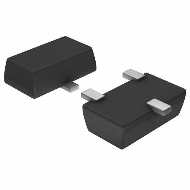
| 描述 | TRANS NPN 20V SOT23F-3两极晶体管 - BJT NPN 20V 7A |
| 产品分类 | 晶体管(BJT) - 单路分离式半导体 |
| 品牌 | Diodes Incorporated |
| 产品手册 | |
| 产品图片 |
|
| rohs | 符合RoHS无铅 / 符合限制有害物质指令(RoHS)规范要求 |
| 产品系列 | 晶体管,两极晶体管 - BJT,Diodes Incorporated ZXTN19020CFFTA- |
| 数据手册 | |
| 产品型号 | ZXTN19020CFFTA |
| RoHS指令信息 | http://diodes.com/download/4349 |
| 不同 Ib、Ic时的 Vce饱和值(最大值) | 175mV @ 280mA,7A |
| 不同 Ic、Vce 时的DC电流增益(hFE)(最小值) | 200 @ 100mA,2V |
| 产品目录绘图 |
|
| 产品目录页面 | |
| 产品种类 | 两极晶体管 - BJT |
| 供应商器件封装 | SOT-23F |
| 其它名称 | ZXTN19020CFFCT |
| 功率-最大值 | 1.5W |
| 包装 | 剪切带 (CT) |
| 发射极-基极电压VEBO | 7 V |
| 商标 | Diodes Incorporated |
| 增益带宽产品fT | 150 MHz |
| 安装类型 | 表面贴装 |
| 安装风格 | SMD/SMT |
| 封装 | Reel |
| 封装/外壳 | SOT-23-3 扁平引线 |
| 封装/箱体 | SOT-23F-3 |
| 工厂包装数量 | 3000 |
| 晶体管极性 | NPN |
| 晶体管类型 | NPN |
| 最大功率耗散 | 2000 mW |
| 最大工作温度 | + 150 C |
| 最大直流电集电极电流 | 7 A |
| 最小工作温度 | - 55 C |
| 标准包装 | 1 |
| 电压-集射极击穿(最大值) | 20V |
| 电流-集电极(Ic)(最大值) | 7A |
| 电流-集电极截止(最大值) | - |
| 直流电流增益hFE最大值 | 500 at 0.1 A at 2 V |
| 直流集电极/BaseGainhfeMin | 45 at 15 A at 2 V |
| 配置 | Single |
| 集电极—发射极最大电压VCEO | 20 V |
| 集电极—基极电压VCBO | 65 V |
| 集电极—射极饱和电压 | 30 mV |
| 集电极连续电流 | 7 A |
| 频率-跃迁 | 150MHz |


- 商务部:美国ITC正式对集成电路等产品启动337调查
- 曝三星4nm工艺存在良率问题 高通将骁龙8 Gen1或转产台积电
- 太阳诱电将投资9.5亿元在常州建新厂生产MLCC 预计2023年完工
- 英特尔发布欧洲新工厂建设计划 深化IDM 2.0 战略
- 台积电先进制程称霸业界 有大客户加持明年业绩稳了
- 达到5530亿美元!SIA预计今年全球半导体销售额将创下新高
- 英特尔拟将自动驾驶子公司Mobileye上市 估值或超500亿美元
- 三星加码芯片和SET,合并消费电子和移动部门,撤换高东真等 CEO
- 三星电子宣布重大人事变动 还合并消费电子和移动部门
- 海关总署:前11个月进口集成电路产品价值2.52万亿元 增长14.8%


PDF Datasheet 数据手册内容提取
ZXTN19020CFF 20V NPN HIGH GAIN POWER TRANSISTOR IN SOT23F Features Mechanical Data BVCEO > 20V Case: SOT23F BVCEX > 65V Case Material: Molded Plastic. ―Green‖ Molding Compound. BVECO > 4.5V UL Flammability Classification Rating 94V-0 IC = 7A Continuous Collector Current Moisture Sensitivity: Level 1 per J-STD-020 Very Low VCE(SAT) < 30mV @ 1A Terminals: Finish – Matte Tin Plated Leads, Solderable per RCE(SAT) = 18mΩ MIL-STD-202, Method 208 1.5W Power Dissipation Weight: 0.012 grams (Approximate) High Forward Blocking Voltage High Gain Applications Complementary PNP Type: ZXTP19020CFF Totally Lead-Free & Fully RoHS Compliant (Notes 1 & 2) MOSFET and IGBT Gate Driving Halogen and Antimony Free. “Green” Device (Note 3) LED Driving Qualified to AEC-Q101 Standards for High Reliability Strobe Flash Motor Drive Micro Buffers Description Advanced process capability has been used to maximize the performance of this transistor. The SOT23F package is compatible with the industry standard SOT23 footprint but offers lower profile and higher dissipation for applications where power density is of utmost importance. SOT23F C E C B B E Top View Device Symbol Top View Pin Configuration Ordering Information (Note 4) Part Number Compliance Marking Reel Size (inches) Tape Width (mm) Quantity per Reel ZXTN19020CFFTA AEC-Q101 1E2 7 8 3,000 Notes: 1. No purposely added lead. Fully EU Directive 2002/95/EC (RoHS) & 2011/65/EU (RoHS 2) compliant. 2. See http://www.diodes.com/quality/lead_free.html for more information about Diodes Incorporated’s definitions of Halogen- and Antimony-free, "Green" and Lead-free. 3. Halogen- and Antimony-free "Green" products are defined as those which contain <900ppm bromine, <900ppm chlorine (<1500ppm total Br + Cl) and <1000ppm antimony compounds. 4. For packaging details, go to our website at http://www.diodes.com/products/packages.html. Marking Information SOT23F 1E2 = Product Type Marking Code 1E2 W YYW = Y= eDaar t:e 0 C~o9d e Marking Y W = Week : A~Z : 1~26 a~z : 27~52 z represents 52 & 53 week ZXTN19020CFF 1 of 7 June 2016 Document number: DS33676 Rev. 2 - 2 www.diodes.com © Diodes Incorporated
ZXTN19020CFF Absolute Maximum Ratings (@TA = +25°C, unless otherwise specified.) Characteristic Symbol Value Unit Collector-Base Voltage VCBO 65 V Collector-Emitter Voltage (Forward Blocking) VCEX 65 V Collector-Emitter Voltage (Base Open) VCEO 20 V Emitter-Collector Voltage (Reverse Blocking) VECO 4.5 V Emitter-Base Voltage VEBO 7 V Continuous Collector Current IC 7 A Peak Pulse Current ICM 15 A Base Current IB 1 A Thermal Characteristics (@TA = +25°C, unless otherwise specified.) Characteristic Symbol Value Unit 0.84 (Note 5) 6.72 1.34 (Note 6) Power Dissipation 10.72 W Linear Derating Factor PD 1.50 mW/°C (Note 7) 12.0 2.0 (Note 8) 16.0 (Note 5) 149 (Note 6) 93 Thermal Resistance, Junction to Ambient (Note 7) RθJA 83 °C/W (Note 8) 60 Thermal Resistance, Junction to Lead (Note 9) RθJL 43.8 °C/W Operating and Storage Temperature Range TJ, TSTG -55 to +150 °C ESD Ratings (Note 10) Characteristic Symbol Value Unit JEDEC Class Electrostatic Discharge – Human Body Model ESD HBM 4,000 V 3A Electrostatic Discharge – Machine Model ESD MM 400 V C Notes: 5. For a device mounted with the exposed collector pad on 15mm x 15mm 1oz copper that is on a single-sided 1.6mm FR-4 PCB; device is measured under still air conditions whilst operating in a steady-state. 6. Same as Note 5, except the device is mounted on 25mm x 25mm 2oz copper. 7. Same as Note 5, except the device is mounted on 50mm x 50mm 2oz copper. 8. Same as Note 7, whilst measured at t < 5 seconds. 9. Thermal resistance from junction to solder-point (at the end of the collector lead). 10. Refer to JEDEC specification JESD22-A114 and JESD22-A115. ZXTN19020CFF 2 of 7 June 2016 Document number: DS33676 Rev. 2 - 2 www.diodes.com © Diodes Incorporated
ZXTN19020CFF Thermal Characteristics and Derating Information 1m A) VCE(sat) 50mmx50mm FR-4, 2oz Cu A) Failure may occur nt ( 10 Limited nt (100μµ in this region e e r r BV =20V ur ur (BR)CEO C 1 C or DC 1s or 10μµ ct 100ms ct e e oll100m 10ms oll 1µμ C Single Pulse C I C10m Tamb=25oC 1ms 100s I C Tamb=25oC BV(BR)CEX=65V 100m 1 10 0 20 40 60 V Collector-Emitter Voltage (V) V Collector-Emitter Voltage (V) CE CE Safe Operating Area Safe Operating Area ) W 80 C/ 70 Tamb=25oC )100 Single Pulse o( 50mmx50mm W T =25oC, ance 5600 DFR=-04., 52oz Cu wer ( 5F0Rma-m4mb, x25o0zm Cmu t o s 40 P si 10 e m al R 2300 D=0.2 Single Pulse mu erm 10 D=0.05 Maxi Th 0 D=0.1 1 100µμ 1m 10m 100m 1 10 100 1k 100μµ 1m 10m 100m 1 10 100 1k Pulse Width (s) Pulse Width (s) Transient Thermal Impedance Pulse Power Dissipation ) 1.6 W ( 1.4 n 50mmx50mm FR-4, tio 1.2 2oz Cu a sip 1.0 25mmx25mm FR-4, s 2oz Cu Di 0.8 er 0.6 w o 0.4 P 15mmx15mm FR-4, x 0.2 1oz Cu a M 0.0 0 20 40 60 80 100 120 140 160 Temperature (oC) Derating Curve ZXTN19020CFF 3 of 7 June 2016 Document number: DS33676 Rev. 2 - 2 www.diodes.com © Diodes Incorporated
ZXTN19020CFF Electrical Characteristics (@TA = +25°C, unless otherwise specified.) Characteristic Symbol Min Typ Max Unit Test Condition OFF CHARACTERISTICS Collector-Base Breakdown Voltage BVCBO 65 85 — V IC = 100µA CBloolclekcintogr -Emitter Breakdown Voltage (Forward BVCEX 65 85 — V IoCr =-1 1V0 <0 µVAB,E R< B0E. 2<5 V1k Ω, Collector-Emitter Breakdown Voltage (Base Open) (Note 11) BVCEO 20 25 — V IC = 10mA Emitter-Base Breakdown Voltage BVEBO 7 8.3 — V IE = 100µA EBmlocitkteinr g–) Collector Breakdown Voltage (Reverse BVECX 6 8.2 — V IoEr =V B1C0 0=µ ±A0,. 2R5BVC < 1kΩ, Emitter – Collector Breakdown Voltage (Base Open) BVECO 4.5 5.3 — V IE = 100µA Collector-Base Cut-off Current ICBO — <—1 5200 µnAA VVCCBB == 5500VV, TA = +100°C Collector-Base Cut-off Current ICEX — <1 100 V-1CVE <= V5B0EV ,< R0.B2E5 V< 1kΩ or Emitter-Base Cut-off Current IEBO — <1 50 nA VEB = 5.6V ON CHARACTERISTICS (Note 11) 200 350 500 IC = 0.1A, VCE = 2V Static Forward Current Transfer Ratio hFE 118000 324200 —— — IICC == 27AA,, VVCCEE == 22VV 45 95 — IC = 15A, VCE = 2V 23 30 IC = 1A, IB = 100mA Collector-Emitter Saturation Voltage VCE(SAT) — 4555 6750 mV IICC == 12AA,, IIBB == 4100mmAA 135 175 IC = 7A, IB = 280mA Base-Emitter Saturation Voltage VBE(SAT) — 960 1050 mV IC = 7A, IB = 280mA Base-Emitter On Voltage VBE(ON) — 840 950 mV IC = 7A, VCE = 2V SMALL SIGNAL CHARACTERISTICS Transition Frequency fT — 150 — MHz IfC = = 5 500MmHAz, VCE = 10V, Input Capacitance CIBO — 315 — pF VEB = 0.5V, f = 1MHz Output Capacitance COBO — 40 50 pF VCB = 10V, f = 1MHz Delay Time tD — 135 — ns RSFatisoller aT Tgimiem eTe i me tttRSF ——— 12818875 ——— nnnsss VIICBC1 = C= 1= -A 1I,B 0 2V =, 10mA Note: 11. Measured under pulsed conditions. Pulse width ≤ 300µs. Duty cycle ≤ 2%. ZXTN19020CFF 4 of 7 June 2016 Document number: DS33676 Rev. 2 - 2 www.diodes.com © Diodes Incorporated
ZXTN19020CFF Typical Electrical Characteristics (@TA = +25°C, unless otherwise specified.) 1 Tamb=25oC 0.4 I/I=10 C B 150oC I/I=100 100m C B 0.3 ) ) V V ( ( 100oC AT) AT)0.2 E(S 10m IC/IB=50 E(S C C V V IC/IB=25 0.1 25oC IC/IB=10 -55oC 1m 0.0 1m 10m 100m 1 10 10m 100m 1 10 I Collector Current (A) I Collector Current (A) C C V v I V v I CE(SAT) C CE(SAT) C 600 1.6 150oC VCE=2V 550 1.2 IC/IB=10 -55oC n1.4 500 )E ai 450 hF 1.0 G1.2 100oC 400 ( V) 25oC alised 01..80 25oC 233505000 al Gain (E(SAT)0.8 Norm00..46 -55oC 112050000 Typic VB0.6 100oC 0.2 50 0.4 150oC 0.0 0 1m 10m 100m 1 10 1m 10m 100m 1 10 I Collector Current (A) I Collector Current (A) C C h v I V v I FE C BE(SAT) C 1.0 VCE=2V -55oC 25oC 0.8 ) V ( N) O 0.6 E( B V 100oC 0.4 150oC 0.2 1m 10m 100m 1 10 I Collector Current (A) C V v I BE(ON) C ZXTN19020CFF 5 of 7 June 2016 Document number: DS33676 Rev. 2 - 2 www.diodes.com © Diodes Incorporated
ZXTN19020CFF Package Outline Dimensions Please see http://www.diodes.com/package-outlines.html for the latest version. SOT23F D c b SOT23F L1 Dim Min Max Typ A 0.80 1.00 0.90 A1 0.00 0.10 0.01 E1 E b 0.35 0.50 0.44 c 0.10 0.20 0.16 D 2.80 3.00 2.90 e 0.95 REF e1 1.90 REF b E 2.30 2.50 2.40 e1 A1 E1 1.50 1.70 1.65 e k 1.20 - - L 0.30 0.65 0.50 L1 0.30 0.50 0.40 L R R 0.05 0.15 - All Dimensions in mm A k Suggested Pad Layout Please see http://www.diodes.com/package-outlines.html for the latest version. SOT23F X C Value Dimensions (in mm) C 0.95 X 0.80 Y 1.110 Y1 Y1 3.000 Y ZXTN19020CFF 6 of 7 June 2016 Document number: DS33676 Rev. 2 - 2 www.diodes.com © Diodes Incorporated
ZXTN19020CFF IMPORTANT NOTICE DIODES INCORPORATED MAKES NO WARRANTY OF ANY KIND, EXPRESS OR IMPLIED, WITH REGARDS TO THIS DOCUMENT, INCLUDING, BUT NOT LIMITED TO, THE IMPLIED WARRANTIES OF MERCHANTABILITY AND FITNESS FOR A PARTICULAR PURPOSE (AND THEIR EQUIVALENTS UNDER THE LAWS OF ANY JURISDICTION). Diodes Incorporated and its subsidiaries reserve the right to make modifications, enhancements, improvements, corrections or other changes without further notice to this document and any product described herein. Diodes Incorporated does not assume any liability arising out of the application or use of this document or any product described herein; neither does Diodes Incorporated convey any license under its patent or trademark rights, nor the rights of others. Any Customer or user of this document or products described herein in such applications shall assume all risks of such use and will agree to hold Diodes Incorporated and all the companies whose products are represented on Diodes Incorporated website, harmless against all damages. Diodes Incorporated does not warrant or accept any liability whatsoever in respect of any products purchased through unauthorized sales channel. Should Customers purchase or use Diodes Incorporated products for any unintended or unauthorized application, Customers shall indemnify and hold Diodes Incorporated and its representatives harmless against all claims, damages, expenses, and attorney fees arising out of, directly or indirectly, any claim of personal injury or death associated with such unintended or unauthorized application. Products described herein may be covered by one or more United States, international or foreign patents pending. Product names and markings noted herein may also be covered by one or more United States, international or foreign trademarks. This document is written in English but may be translated into multiple languages for reference. Only the English version of this document is the final and determinative format released by Diodes Incorporated. LIFE SUPPORT Diodes Incorporated products are specifically not authorized for use as critical components in life support devices or systems without the express written approval of the Chief Executive Officer of Diodes Incorporated. As used herein: A. Life support devices or systems are devices or systems which: 1. are intended to implant into the body, or 2. support or sustain life and whose failure to perform when properly used in accordance with instructions for use provided in the labeling can be reasonably expected to result in significant injury to the user. B. A critical component is any component in a life support device or system whose failure to perform can be reasonably expected to cause the failure of the life support device or to affect its safety or effectiveness. Customers represent that they have all necessary expertise in the safety and regulatory ramifications of their life support devices or systems, and acknowledge and agree that they are solely responsible for all legal, regulatory and safety-related requirements concerning their products and any use of Diodes Incorporated products in such safety-critical, life support devices or systems, notwithstanding any devices- or systems-related information or support that may be provided by Diodes Incorporated. Further, Customers must fully indemnify Diodes Incorporated and its representatives against any damages arising out of the use of Diodes Incorporated products in such safety-critical, life support devices or systems. Copyright © 2016, Diodes Incorporated www.diodes.com ZXTN19020CFF 7 of 7 June 2016 Document number: DS33676 Rev. 2 - 2 www.diodes.com © Diodes Incorporated
Mouser Electronics Authorized Distributor Click to View Pricing, Inventory, Delivery & Lifecycle Information: D iodes Incorporated: ZXTN19020CFFTA