ICGOO在线商城 > 分立半导体产品 > 晶体管 - 双极 (BJT) - 单 > STBV45G-AP
,TO-226_straightlead.jpg)
 Datasheet下载
- 型号: STBV45G-AP
- 制造商: STMicroelectronics
- 库位|库存: xxxx|xxxx
- 要求:
| 数量阶梯 | 香港交货 | 国内含税 |
| +xxxx | $xxxx | ¥xxxx |
查看当月历史价格
查看今年历史价格
STBV45G-AP产品简介:
ICGOO电子元器件商城为您提供STBV45G-AP由STMicroelectronics设计生产,在icgoo商城现货销售,并且可以通过原厂、代理商等渠道进行代购。 STBV45G-AP价格参考。STMicroelectronicsSTBV45G-AP封装/规格:晶体管 - 双极 (BJT) - 单, Bipolar (BJT) Transistor NPN 400V 750mA 950mW Through Hole TO-92AP。您可以下载STBV45G-AP参考资料、Datasheet数据手册功能说明书,资料中有STBV45G-AP 详细功能的应用电路图电压和使用方法及教程。
STMicroelectronics(意法半导体)生产的STBV45G-AP是一款NPN型双极结型晶体管(BJT),属于单BJT器件,广泛应用于中等功率开关和放大电路中。该器件采用SOT-89-3封装,具有良好的热稳定性和较高的可靠性,适合在工业、消费类电子及汽车电子等领域使用。

典型应用场景包括:
1. 电源管理电路:用于DC-DC转换器中的开关控制,实现电压调节与能量转换。
2. LED驱动电路:作为恒流源或开关元件,控制LED的亮灭与亮度调节,适用于照明系统。
3. 电机驱动与继电器控制:在小功率电机或电磁继电器的驱动电路中,用作开关元件,实现微控制器对高功率负载的控制。
4. 信号放大:在音频或传感器信号处理电路中,用于小信号放大,提升信号强度。
5. 消费类电子产品:如电视、机顶盒、充电器等设备中的接口驱动与电源切换电路。

STBV45G-AP具备较高的直流电流增益和快速开关特性,同时具有较低的饱和压降,有助于提高系统效率并减少发热。其坚固的封装设计也增强了在恶劣环境下的稳定性,特别适用于空间受限但需一定功率处理能力的应用场合。综合来看,该器件是一款性能可靠、应用广泛的通用型中功率晶体管。
| 参数 | 数值 |
| 产品目录 | |
| 描述 | TRANS NPN 400V FAST SW TO-92AP |
| 产品分类 | 晶体管(BJT) - 单路 |
| 品牌 | STMicroelectronics |
| 数据手册 | |
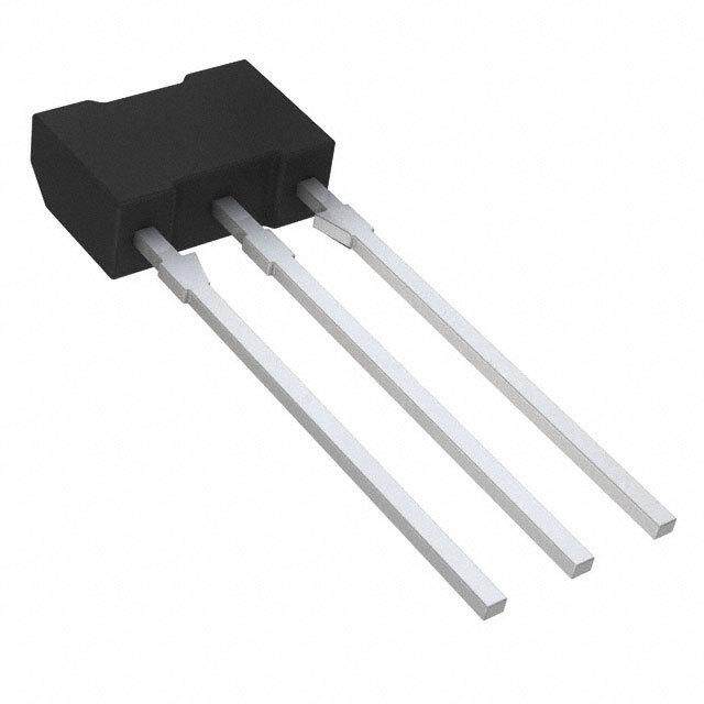
| 产品图片 |
|
| 产品型号 | STBV45G-AP |
| rohs | 无铅 / 符合限制有害物质指令(RoHS)规范要求 |
| 产品系列 | - |
| 不同 Ib、Ic时的 Vce饱和值(最大值) | 1.5V @ 135mA,400mA |
| 不同 Ic、Vce 时的DC电流增益(hFE)(最小值) | 5 @ 400mA,5V |
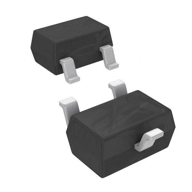
| 供应商器件封装 | TO-92AP |
| 其它名称 | 497-12549-1 |
| 其它有关文件 | http://www.st.com/web/catalog/sense_power/FM100/CL822/SC1229/PF64540?referrer=70071840 |
| 功率-最大值 | 950mW |
| 包装 | 剪切带 (CT) |
| 安装类型 | 通孔 |
| 封装/外壳 | TO-226-3、TO-92-3(TO-226AA)成形引线 |
| 晶体管类型 | NPN |
| 标准包装 | 1 |
| 电压-集射极击穿(最大值) | 400V |
| 电流-集电极(Ic)(最大值) | 750mA |
| 电流-集电极截止(最大值) | 250µA |
| 频率-跃迁 | - |


- 商务部:美国ITC正式对集成电路等产品启动337调查
- 曝三星4nm工艺存在良率问题 高通将骁龙8 Gen1或转产台积电
- 太阳诱电将投资9.5亿元在常州建新厂生产MLCC 预计2023年完工
- 英特尔发布欧洲新工厂建设计划 深化IDM 2.0 战略
- 台积电先进制程称霸业界 有大客户加持明年业绩稳了
- 达到5530亿美元!SIA预计今年全球半导体销售额将创下新高
- 英特尔拟将自动驾驶子公司Mobileye上市 估值或超500亿美元
- 三星加码芯片和SET,合并消费电子和移动部门,撤换高东真等 CEO
- 三星电子宣布重大人事变动 还合并消费电子和移动部门
- 海关总署:前11个月进口集成电路产品价值2.52万亿元 增长14.8%


PDF Datasheet 数据手册内容提取
STBV45 High voltage fast-switching NPN power transistor Features ■ High voltage capability ) ■ Low spread of dynamic parameters s ( ■ Minimum lot-to-lot spread for reliable operation ct u ■ Very high switching speed d o Applications r P ■ Compact fluorescent lamps (CFLs) e t e ■ SMPS for battery charger TO-92 TO-92AP l o s Description b O Figure 1. Internal schematic diagram The device is manufactured using high voltage - multi epitaxial planar technology for high switc hing ) speeds and high voltage capability. It usess a ( cellular emitter structure with planar etdge c termination to enhance switchingu speeds while maintaining the wide RBSOA.d o The STBV45G and STBV45G-AP are supplied r using halogen-free moP lding compound. e t e l o s b O T able 1. Device summary Order codes Marking Package Packaging STBV45 BV45 TO-92 Bulk STBV45G BV45G TO-92 Bulk STBV45-AP BV45 TO-92AP Ammopack STBV45G-AP BV45G TO-92AP Ammopack October 2008 Rev 6 1/10 www.st.com 10
Electrical ratings STBV45 1 Electrical ratings Table 2. Absolute maximum rating Symbol Parameter Value Unit V Collector-emitter voltage (V = 0) 700 V CES BE V Collector-emitter voltage (I = 0) 400 V CEO B V Emitter-base voltage (I = 0) 9 V EBO C I Collector current 0.75 A C I Collector peak current (t < 5 ms) 1.5 )A CM P s I Base current 0.4 ( A B t c I Base peak current (t < 5 ms) 0.75u A BM P d PTOT Total dissipation at Tc = 25 °C o 0.95 W r T Storage temperature P -65 to 150 stg °C T Max. operating junction temperature e 150 J t e Table 3. Thermal data ol s Symbol Parameter b Value Unit O R Thermal resistance junction-case__________max 131.6 °C/W thj-case - ) s ( t c u d o r P e t e l o s b O 2/10
STBV45 Electrical characteristics 2 Electrical characteristics (T = 25 °C; unless otherwise specified) case Table 4. Electrical characteristics Symbol Parameter Test conditions Min. Typ. Max. Unit Collector cut-off current I V = 700 V 250 µA CES (V = 0) CE BE Emitter cut-off current I V = 9 V 1 mA EBO (IC = 0) EB ) s V Collector-emitter sustaining ( CEO(sus) I = 1 mA 400 t V (1) voltage (I = 0) C c B u I = 0.2 A I = 40 mA d 0.2 0.5 V C B V (1) Collector-emitter saturation I = 0.3 A I = 75 mA o 0.3 1 V CE(sat) voltage C B r I = 0.4 A I = 135 mP A 0.4 1.5 V C B V (1) Base-emitter saturation IC = 0.2 A ItB =e 40 mA 1 V BE(sat) voltage I = 0.3 A e I = 75 mA 1.2 V C B l o IC = 0.5s mA VCE = 2 V 12 h DC current gain I =b 0.2 A V = 5 V 10 30 FE C CE O IC = 0.4 A VCE = 5 V 5 20 - Inductive load I = 0.2 A _ V = 300 V ) C clamp t Fall time s I = -I = 40 mA 0.3 µs f ( B1 B2 t L= 3 mH Figure 8. c u 1. Pulsed duration = 300 µs, duty cycle ≤ 1.5% d o r P 2.1 Electrical characteristics (curves) e e t l Figure 2. Safe operating area Figure 3. Derating curve o s b O 3/10
Electrical characteristics STBV45 Figure 4. DC current gain Figure 5. DC current gain ) s ( t c u Figure 6. Collector-emitter saturation Figure 7. Base-emitter saturation d voltage voltage o r P e t e l o s b O - ) s ( t c u d o r P e t e l o s b O 4/10
STBV45 Electrical characteristics 2.2 Test circuit Figure 8. Inductive load switching test circuit ) s ( 1) Fast electronic switch t c 2) Non-inductive resistor u d 3) Fast recovery rectifier o r P e t e l o s b O - ) s ( t c u d o r P e t e l o s b O 5/10
Package mechanical data STBV45 3 Package mechanical data In order to meet environmental requirements, ST offers these devices in ECOPACK® packages. These packages have a lead-free second level interconnect . The category of second level interconnect is marked on the package and on the inner box label, in compliance with JEDEC Standard JESD97. The maximum ratings related to soldering conditions are also marked on the inner box label. ECOPACK is an ST trademark. ECOPACK specifications are available at: www.st.com ) s ( t c u d o r P e t e l o s b O - ) s ( t c u d o r P e t e l o s b O 6/10
STBV45 Package mechanical data TO-92 bulk shipment mechanical data mm. DIM. MIN. TYP MAX. A 4.32 4.95 ) s b 0.36 0.51 ( t c D 4.45 4.95 u d E 3.30 3.94 o e 2.41 r 2.67 P e1 1.14 e 1.40 t L 12.70 e 15.49 l o R 2.16 2.41 s b S1 0.92 1.52 O W 0.41 0.56 - V ) 5o s ( t c u d o r P e t e l o s b O 0102782 D 7/10
Package mechanical data STBV45 TO-92 ammopack shipment (suffix”-AP”) mechanical data mm Dim. Min Typ Max A1 4.80 T 3.80 T1 1.60 T2 2.30 d 0.48 P0 12.50 12.70 12.90 P2 5.65 6.35 7.05 ) s F1,F2 2.44 2.54 2.94 ( F3 4.98 5.08 5.48 t c delta H -2.00 u2.00 W 17.50 18.00 d 19.00 W0 5.70 6.00 o 6.30 W1 8.50 9.00 r 9.25 W2 P 0.50 H 18.50 20.50 e H3 0.5 1 1.5 t H0 15.50 16.00e 16.50 H1 ol 25.00 D0 3.80 s 4.00 4.20 t b 0.90 L O 11.00 I1 3.00 delta P -1.00 - 1.00 ) s ( t c u d o r P e t e l o s b O 0050910S 8/10
STBV45 Revision history 4 Revision history T able 5. Document revision history Date Revision Changes 13-Jul-2004 4 03-Jul-2008 5 Added halogen-free molding compound package. 22-Oct-2008 6 Updated Table2 on page2 and Table4 on page3 ) s ( t c u d o r P e t e l o s b O - ) s ( t c u d o r P e t e l o s b O 9/10
STBV45 Please Read Carefully: ) s ( t c Information in this document is provided solely in connection with ST products. STMicroelectronics NV and its subsidiauries (“ST”) reserve the right to make changes, corrections, modifications or improvements, to this document, and the products and servicdes described herein at any time, without notice. o All ST products are sold pursuant to ST’s terms and conditions of sale. P r Purchasers are solely responsible for the choice, selection and use of the ST products and servi ces described herein, and ST assumes no e liability whatsoever relating to the choice, selection or use of the ST products and services described herein. t e No license, express or implied, by estoppel or otherwise, to any intellectual property rights is granted under this document. If any part of this l document refers to any third party products or services it shall not be deemed a licoense grant by ST for the use of such third party products or services, or any intellectual property contained therein or considered as a wsarranty covering the use in any manner whatsoever of such third party products or services or any intellectual property contained therebin. O - UNLESS OTHERWISE SET FORTH IN ST’S TERMS AN D CONDITIONS OF SALE ST DISCLAIMS ANY EXPRESS OR IMPLIED WARRANTY WITH RESPECT TO THE USE AND/OR) SALE OF ST PRODUCTS INCLUDING WITHOUT LIMITATION IMPLIED s WARRANTIES OF MERCHANTABILITY, FITNESS( FOR A PARTICULAR PURPOSE (AND THEIR EQUIVALENTS UNDER THE LAWS OF ANY JURISDICTION), OR INFRINGEMENT OtF ANY PATENT, COPYRIGHT OR OTHER INTELLECTUAL PROPERTY RIGHT. c UNLESS EXPRESSLY APPROVED IN uWRITING BY AN AUTHORIZED ST REPRESENTATIVE, ST PRODUCTS ARE NOT RECOMMENDED, AUTHORIZED OR WdARRANTED FOR USE IN MILITARY, AIR CRAFT, SPACE, LIFE SAVING, OR LIFE SUSTAINING APPLICATIONS, NOR IN PRODUoCTS OR SYSTEMS WHERE FAILURE OR MALFUNCTION MAY RESULT IN PERSONAL INJURY, DEATH, OR SEVERE PROPERrTY OR ENVIRONMENTAL DAMAGE. ST PRODUCTS WHICH ARE NOT SPECIFIED AS "AUTOMOTIVE P GRADE" MAY ONLY BE USED IN AUTOMOTIVE APPLICATIONS AT USER’S OWN RISK. e t e Resale of ST products with provisions different from the statements and/or technical features set forth in this document shall immediately void l any warraonty granted by ST for the ST product or service described herein and shall not create or extend in any manner whatsoever, any liabilitsy of ST. b O ST and the ST logo are trademarks or registered trademarks of ST in various countries. Information in this document supersedes and replaces all information previously supplied. The ST logo is a registered trademark of STMicroelectronics. All other names are the property of their respective owners. © 2008 STMicroelectronics - All rights reserved STMicroelectronics group of companies Australia - Belgium - Brazil - Canada - China - Czech Republic - Finland - France - Germany - Hong Kong - India - Israel - Italy - Japan - Malaysia - Malta - Morocco - Singapore - Spain - Sweden - Switzerland - United Kingdom - United States of America www.st.com 10/10