ICGOO在线商城 > 分立半导体产品 > 晶体管 - 双极 (BJT) - 单 > MSA1162GT1G

 Datasheet下载
- 型号: MSA1162GT1G
- 制造商: ON Semiconductor
- 库位|库存: xxxx|xxxx
- 要求:
| 数量阶梯 | 香港交货 | 国内含税 |
| +xxxx | $xxxx | ¥xxxx |
查看当月历史价格
查看今年历史价格
MSA1162GT1G产品简介:
ICGOO电子元器件商城为您提供MSA1162GT1G由ON Semiconductor设计生产,在icgoo商城现货销售,并且可以通过原厂、代理商等渠道进行代购。 MSA1162GT1G价格参考¥0.17-¥0.20。ON SemiconductorMSA1162GT1G封装/规格:晶体管 - 双极 (BJT) - 单, 双极 (BJT) 晶体管 PNP 50V 100mA 80MHz 200mW 表面贴装 SC-59。您可以下载MSA1162GT1G参考资料、Datasheet数据手册功能说明书,资料中有MSA1162GT1G 详细功能的应用电路图电压和使用方法及教程。
ON Semiconductor(安森美)的MSA1162GT1G是一款NPN型双极结型晶体管(BJT),属于通用放大和开关应用的小信号晶体管。该器件采用SOT-23封装,具有小型化、高可靠性和良好热稳定性的特点,适用于空间受限的便携式电子设备。

MSA1162GT1G主要应用于以下场景:
1. 便携式消费类电子产品:如智能手机、平板电脑、可穿戴设备中用于信号放大或小电流开关控制。
2. 电源管理电路:在DC-DC转换器、电压检测电路或LED驱动中作为开关元件,实现低功耗控制。
3. 逻辑电路与接口电路:用于电平转换、逻辑门驱动或微控制器输出信号的缓冲与放大。
4. 传感器信号调理:在各类传感器(如温度、光感、运动传感器)输出级中作为放大或开关元件,提升信号驱动能力。
5. 通信设备:应用于无线模块、射频前端控制电路中的小信号处理。

该晶体管具备较高的直流电流增益和快速开关响应特性,同时符合RoHS环保标准,并通过了汽车级可靠性认证(AEC-Q101),因此也适用于汽车电子中的非动力系统,如车内照明控制、信息娱乐系统模块等。

综上,MSA1162GT1G凭借其小型封装、稳定性能和广泛的工作范围,成为消费电子、工业控制和汽车电子等领域中小信号处理的理想选择。
| 参数 | 数值 |
| 产品目录 | |
| 描述 | TRANS GP PNP 50V SC59两极晶体管 - BJT 100mA 60V PNP |
| 产品分类 | 晶体管(BJT) - 单路分离式半导体 |
| 品牌 | ON Semiconductor |
| 产品手册 | |
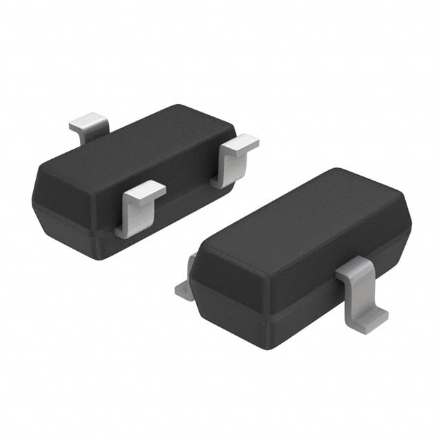
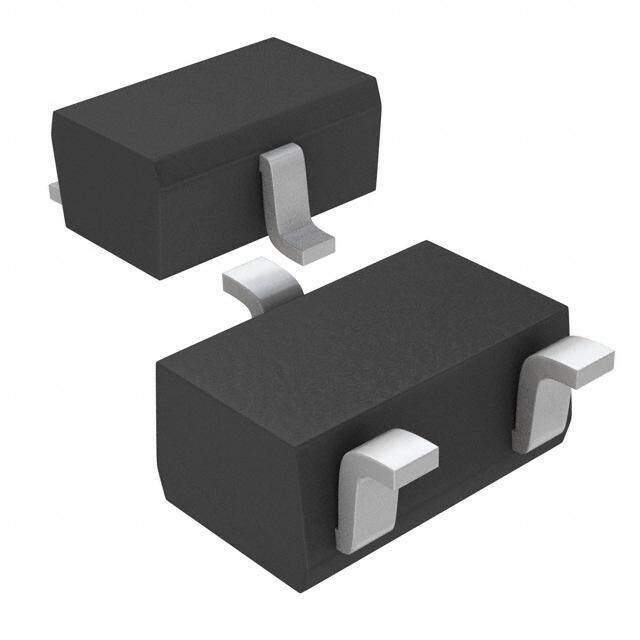
| 产品图片 |
|
| rohs | 符合RoHS无铅 / 符合限制有害物质指令(RoHS)规范要求 |
| 产品系列 | 晶体管,两极晶体管 - BJT,ON Semiconductor MSA1162GT1G- |
| 数据手册 | |
| 产品型号 | MSA1162GT1G |
| PCN设计/规格 | |
| 不同 Ib、Ic时的 Vce饱和值(最大值) | 500mV @ 10mA,100mA |
| 不同 Ic、Vce 时的DC电流增益(hFE)(最小值) | 200 @ 2mA,6V |
| 产品种类 | 两极晶体管 - BJT |
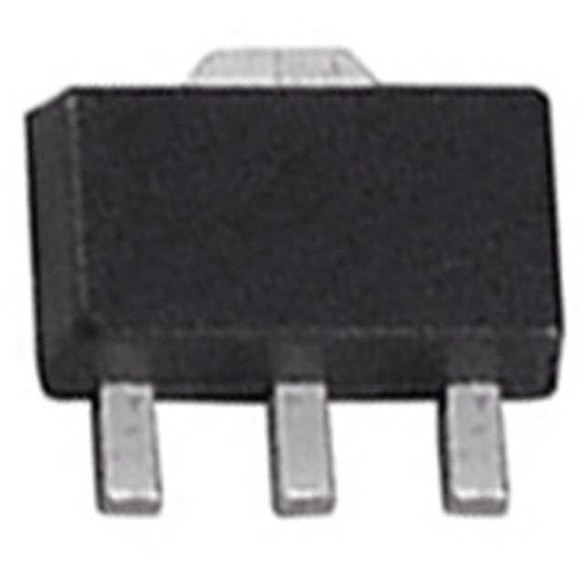
| 供应商器件封装 | SC-59 |
| 其它名称 | MSA1162GT1GOSCT |
| 功率-最大值 | 200mW |
| 包装 | 剪切带 (CT) |
| 发射极-基极电压VEBO | 7 V |
| 商标 | ON Semiconductor |
| 增益带宽产品fT | 80 MHz |
| 安装类型 | 表面贴装 |
| 安装风格 | SMD/SMT |
| 封装 | Reel |
| 封装/外壳 | TO-236-3,SC-59,SOT-23-3 |
| 封装/箱体 | SC-59-3 |
| 工厂包装数量 | 3000 |
| 晶体管极性 | PNP |
| 晶体管类型 | PNP |
| 最大功率耗散 | 0.2 W |
| 最大工作温度 | + 150 C |
| 最大直流电集电极电流 | 0.1 A |
| 最小工作温度 | - 55 C |
| 标准包装 | 1 |
| 电压-集射极击穿(最大值) | 50V |
| 电流-集电极(Ic)(最大值) | 100mA |
| 电流-集电极截止(最大值) | 100nA |
| 直流集电极/BaseGainhfeMin | 200 |
| 系列 | MSA1162 |
| 配置 | Single |
| 集电极—发射极最大电压VCEO | 50 V |
| 集电极—基极电压VCBO | 60 V |
| 集电极—射极饱和电压 | 0.5 V |
| 集电极连续电流 | 0.1 uA |
| 频率-跃迁 | 80MHz |


- 商务部:美国ITC正式对集成电路等产品启动337调查
- 曝三星4nm工艺存在良率问题 高通将骁龙8 Gen1或转产台积电
- 太阳诱电将投资9.5亿元在常州建新厂生产MLCC 预计2023年完工
- 英特尔发布欧洲新工厂建设计划 深化IDM 2.0 战略
- 台积电先进制程称霸业界 有大客户加持明年业绩稳了
- 达到5530亿美元!SIA预计今年全球半导体销售额将创下新高
- 英特尔拟将自动驾驶子公司Mobileye上市 估值或超500亿美元
- 三星加码芯片和SET,合并消费电子和移动部门,撤换高东真等 CEO
- 三星电子宣布重大人事变动 还合并消费电子和移动部门
- 海关总署:前11个月进口集成电路产品价值2.52万亿元 增长14.8%


PDF Datasheet 数据手册内容提取
MSA1162GT1G General Purpose Amplifier Transistors PNP Surface Mount Features • http://onsemi.com Moisture Sensitivity Level: 1 • This is a Pb−Free Device COLLECTOR 3 MAXIMUM RATINGS (TA = 25°C) Rating Symbol Value Unit Collector−Base Voltage V(BR)CBO 60 Vdc Collector−Emitter Voltage V(BR)CEO 50 Vdc 1 2 Emitter−Base Voltage V(BR)EBO 7.0 Vdc BASE EMITTER Collector Current − Continuous IC 100 mAdc Collector Current − Peak IC(P) 200 mAdc THERMAL CHARACTERISTICS Characteristic Symbol Max Unit Power Dissipation PD 200 mW SC−59 CASE 318D Junction Temperature TJ 150 °C STYLE 1 Storage Temperature Tstg −55 to +150 °C Stresses exceeding Maximum Ratings may damage the device. Maximum MARKING DIAGRAM Ratings are stress ratings only. Functional operation above the Recommended Operating Conditions is not implied. Extended exposure to stresses above the Recommended Operating Conditions may affect device reliability. 62G M(cid:2) ELECTRICAL CHARACTERISTICS (TA = 25°C unless otherwise noted) (cid:2) Characteristic Symbol Min Max Unit 1 Collector−Emitter Breakdown Voltage V(BR)CEO 50 − Vdc (IC = 2.0 mAdc, IB = 0) 62G =Device Code M = Date Code* C(ICo l=le c1t0o r(cid:2)−ABdacs,e I EB =re 0a)kdown Voltage V(BR)CBO 60 − Vdc (cid:2) =Pb−Free Package (Note: Microdot may be in either location) Emitter−Base Breakdown Voltage V(BR)EBO 7.0 − Vdc (IE = 10 (cid:2)Adc, IC = 0) *Date Code orientation may vary depending upon manufacturing location. Collector−Base Cutoff Current ICBO − 0.1 (cid:2)Adc (VCB = 45 Vdc, IE = 0) Collector−Emitter Cutoff Current ICEO (VCE = 10 Vdc, IB = 0) − 0.1 (cid:2)Adc ORDERING INFORMATION (VCE = 30 Vdc, IB = 0) − 2.0 (cid:2)Adc (VCE = 30 Vdc, IB = 0, TA = 80°C) − 1.0 mAdc Device Package Shipping† DC Current Gain (Note 1) hFE − MSA1162GT1G SC−59 3000/Tape & Reel (VCE = 6.0 Vdc, IC = 2.0 mAdc) 200 400 (Pb−Free) Collector−Emitter Saturation Voltage VCE(sat) − 0.5 Vdc (IC = 100 mAdc, IB = 10 mAdc) †For information on tape and reel specifications, including part orientation and tape sizes, please Current−Gain − Bandwidth Product fT MHz refer to our Tape and Reel Packaging Specifications (IC = 1 mA, VCE = 10.0 V, f = 10 MHz) 80 − Brochure, BRD8011/D. 1. Pulse Test: Pulse Width ≤ 300 (cid:2)s, D.C. ≤ 2%. © Semiconductor Components Industries, LLC, 2013 1 Publication Order Number: October, 2013 − Rev. 7 MSA1162GT1/D
MSA1162GT1G TYPICAL ELECTRICAL CHARACTERISTICS −200 1000 −2.0 mA −1.5 mA A) m NT (−160 −1.0 mA AIN TA = 100°C E G R T UR−120 EN 25°C −25°C C −0.5 mA R R R100 O U CT −80 C C LLE IB = −0.2 mA , DE CO −40 hF I, C TA = 25°C VCE = −1.0 V 0 10 0 −1 −2 −3 −4 −5 −6 −1 −10 −100 −1000 VCE, COLLECTOR−EMITTER VOLTAGE (V) IC, COLLECTOR CURRENT (mA) Figure 1. Collector Saturation Region Figure 2. DC Current Gain V) 1000 E ( −1 G A LT IC/IB = 10 N TA = 100°C VO GAI OR TA = 100°C RENT 25°C −25°C LLECT 25°C −25°C R 100 O −0.1 U C C C UM D M , E XI hF MA 10 VCE = −6.0 V , E(sat)−0.01 −1 −10 −100 −1000 VC −1 −10 −100 −1000 IC, COLLECTOR CURRENT (mA) IC, COLLECTOR CURRENT (mA) Figure 3. DC Current Gain Figure 4. V versus I CE(sat) C −10 −10,000 COMMON EMITTER 25°C ON VCE = 6 V TA = 100°C TI A)−1000 A (cid:2) TURV) NT ( −25°C SAE ( RE −100 TTER OLTAG−1 E CUR −10 MIV S E A − B ASE TA = 25°C I, B −1 B IC/IB = 10 −0.1 −0.1 −1 −10 −100 −1000 0 −0.1 −0.2 −0.3 −0.4 −0.5 −0.6 −0.7 −0.8 −0.9 −1 IC, COLLECTOR CURRENT (mA) VBE, BASE−EMITTER VOLTAGE (V) Figure 5. V versus I Figure 6. Base−Emitter Voltage BE(sat) C http://onsemi.com 2
MSA1162GT1G PACKAGE DIMENSIONS SC−59 CASE 318D−04 ISSUE H D NOTES: (cid:2)(cid:3)1. DIMENSIONING AND TOLERANCING PER ANSI Y14.5M, 1982. (cid:2)(cid:3)2. CONTROLLING DIMENSION: MILLIMETER. MILLIMETERS INCHES 3 DIM MIN NOM MAX MIN NOM MAX HE 1 2 E AA1 01..0010 01..0165 10..3100 00..003091 00..004052 00..005014 b 0.35 0.43 0.50 0.014 0.017 0.020 c 0.09 0.14 0.18 0.003 0.005 0.007 D 2.70 2.90 3.10 0.106 0.114 0.122 b E 1.30 1.50 1.70 0.051 0.059 0.067 e e 1.70 1.90 2.10 0.067 0.075 0.083 L 0.20 0.40 0.60 0.008 0.016 0.024 HE 2.50 2.80 3.00 0.099 0.110 0.118 C STYLE 1: A PIN 1.BASE 2.EMITTER 3.COLLECTOR L A1 SOLDERING FOOTPRINT* 0.95 0.95 0.037 0.037 2.4 0.094 1.0 0.039 0.8 (cid:2) mm (cid:3) SCALE 10:1 0.031 inches *For additional information on our Pb−Free strategy and soldering details, please download the ON Semiconductor Soldering and Mounting Techniques Reference Manual, SOLDERRM/D. ON Semiconductor and are registered trademarks of Semiconductor Components Industries, LLC (SCILLC). SCILLC owns the rights to a number of patents, trademarks, copyrights, trade secrets, and other intellectual property. A listing of SCILLC’s product/patent coverage may be accessed at www.onsemi.com/site/pdf/Patent−Marking.pdf. SCILLC reserves the right to make changes without further notice to any products herein. SCILLC makes no warranty, representation or guarantee regarding the suitability of its products for any particular purpose, nor does SCILLC assume any liability arising out of the application or use of any product or circuit, and specifically disclaims any and all liability, including without limitation special, consequential or incidental damages. “Typical” parameters which may be provided in SCILLC data sheets and/or specifications can and do vary in different applications and actual performance may vary over time. All operating parameters, including “Typicals” must be validated for each customer application by customer’s technical experts. SCILLC does not convey any license under its patent rights nor the rights of others. SCILLC products are not designed, intended, or authorized for use as components in systems intended for surgical implant into the body, or other applications intended to support or sustain life, or for any other application in which the failure of the SCILLC product could create a situation where personal injury or death may occur. Should Buyer purchase or use SCILLC products for any such unintended or unauthorized application, Buyer shall indemnify and hold SCILLC and its officers, employees, subsidiaries, affiliates, and distributors harmless against all claims, costs, damages, and expenses, and reasonable attorney fees arising out of, directly or indirectly, any claim of personal injury or death associated with such unintended or unauthorized use, even if such claim alleges that SCILLC was negligent regarding the design or manufacture of the part. SCILLC is an Equal Opportunity/Affirmative Action Employer. This literature is subject to all applicable copyright laws and is not for resale in any manner. PUBLICATION ORDERING INFORMATION LITERATURE FULFILLMENT: N. American Technical Support: 800−282−9855 Toll Free ON Semiconductor Website: www.onsemi.com Literature Distribution Center for ON Semiconductor USA/Canada P.O. Box 5163, Denver, Colorado 80217 USA Europe, Middle East and Africa Technical Support: Order Literature: http://www.onsemi.com/orderlit Phone: 303−675−2175 or 800−344−3860 Toll Free USA/Canada Phone: 421 33 790 2910 Fax: 303−675−2176 or 800−344−3867 Toll Free USA/Canada Japan Customer Focus Center For additional information, please contact your local Email: orderlit@onsemi.com Phone: 81−3−5817−1050 Sales Representative http://onsemi.com MSA1162GT1/D 3
Mouser Electronics Authorized Distributor Click to View Pricing, Inventory, Delivery & Lifecycle Information: O N Semiconductor: MSA1162GT1G