ICGOO在线商城 > 射频/IF 和 RFID > RF 开关 > PE42520MLBA-Z
 Datasheet下载
- 型号: PE42520MLBA-Z
- 制造商: Peregrine
- 库位|库存: xxxx|xxxx
- 要求:
| 数量阶梯 | 香港交货 | 国内含税 |
| +xxxx | $xxxx | ¥xxxx |
查看当月历史价格
查看今年历史价格
PE42520MLBA-Z产品简介:
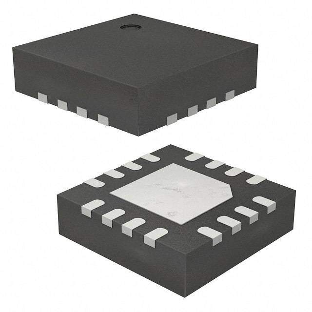
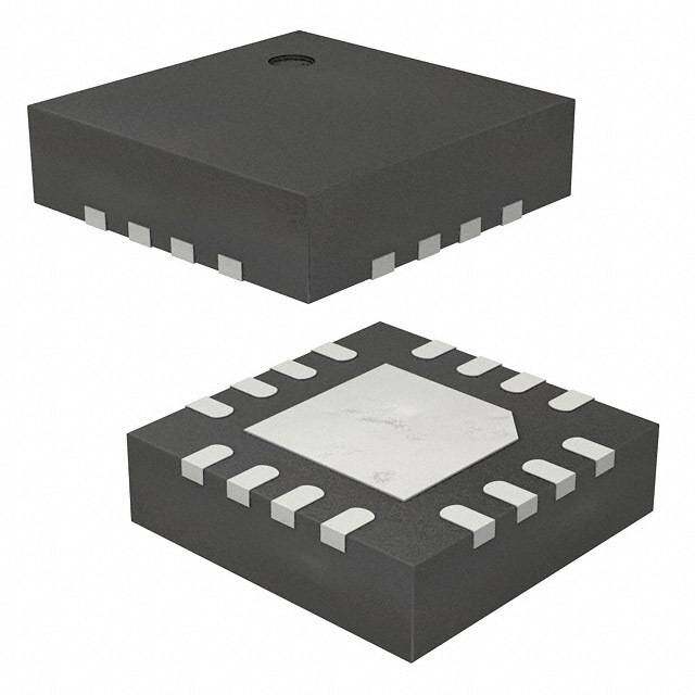
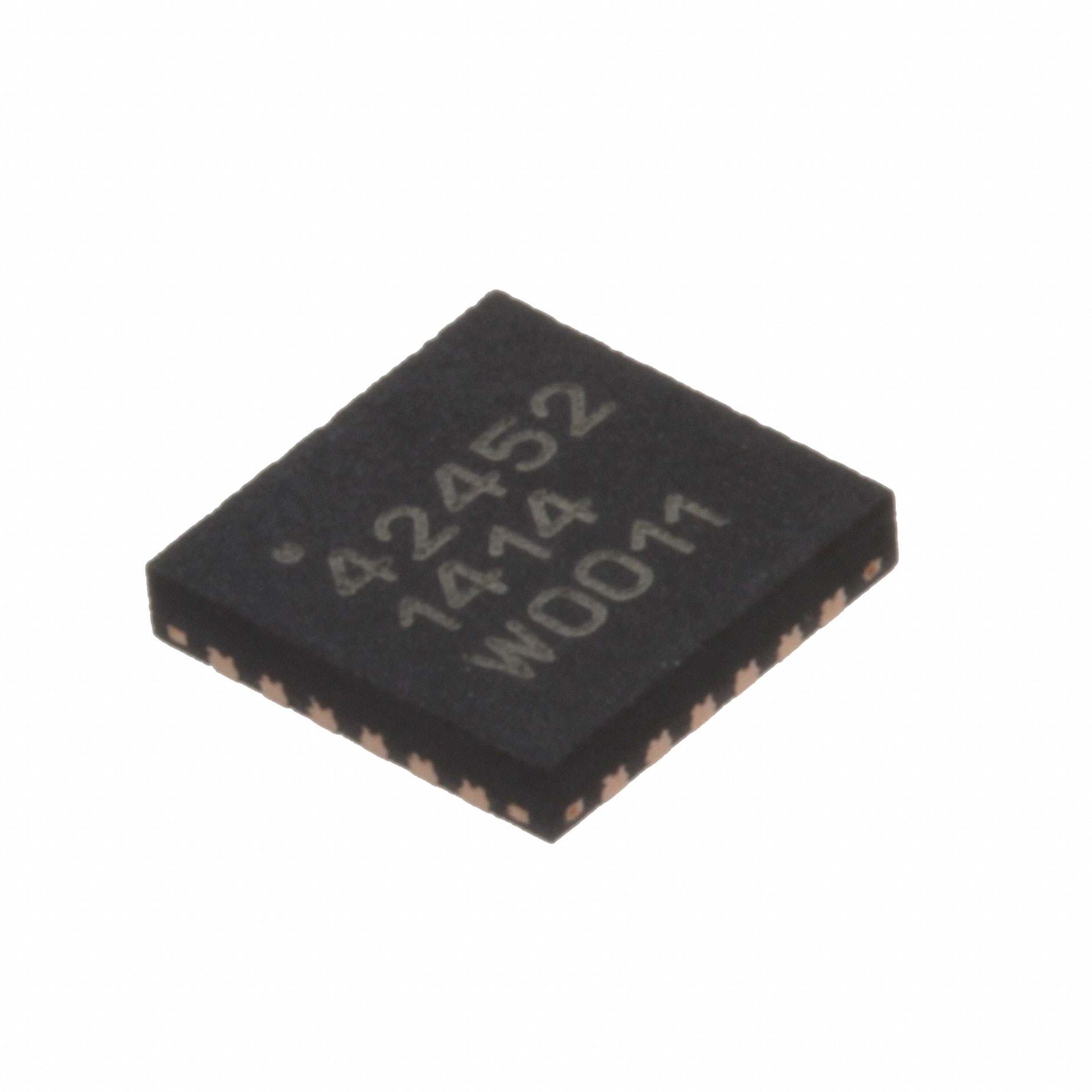
ICGOO电子元器件商城为您提供PE42520MLBA-Z由Peregrine设计生产,在icgoo商城现货销售,并且可以通过原厂、代理商等渠道进行代购。 PE42520MLBA-Z价格参考。PeregrinePE42520MLBA-Z封装/规格:RF 开关, 射频开关 IC ATE SPDT 13GHz 50 欧姆 16-QFN(3x3)。您可以下载PE42520MLBA-Z参考资料、Datasheet数据手册功能说明书,资料中有PE42520MLBA-Z 详细功能的应用电路图电压和使用方法及教程。
PE42520MLBA-Z 是由 pSemi(现为 Qorvo 的一部分)制造的一款高性能 RF 开关,广泛应用于无线通信、雷达、测试设备等领域。以下是该型号的主要应用场景:

 1. 无线通信系统
PE42520MLBA-Z 在无线通信系统中主要用于信号路径的选择和切换。它可以在不同的射频通道之间快速切换,适用于多频段或多模式的无线设备。例如,在蜂窝基站、Wi-Fi 路由器和移动终端中,这款开关可以实现天线与不同射频链路之间的高效切换,确保信号传输的稳定性和可靠性。

 2. 雷达系统
在雷达应用中,PE42520MLBA-Z 可用于发射和接收信号的切换。雷达系统通常需要在短时间内快速切换工作模式,从发射状态切换到接收状态,以避免自干扰并提高检测精度。该开关具有低插入损耗和高隔离度的特点,能够在高频段下保持优异的性能,适合用于军事雷达、气象雷达等场合。

 3. 测试与测量设备
在实验室或生产线上,PE42520MLBA-Z 常用于测试与测量设备中,帮助工程师在不同频率或信号源之间进行快速切换。其低功耗和高可靠性使得它成为自动化测试系统中的理想选择,尤其是在需要频繁切换信号路径的场景下,能够显著提高测试效率。

 4. 物联网 (IoT) 设备
随着物联网设备的普及,PE42520MLBA-Z 还可用于智能传感器、智能家居设备等低功耗应用场景。它的小尺寸和低功耗特性使其非常适合集成到小型化、便携式的无线模块中,支持多种通信协议(如蓝牙、Zigbee 等),并能有效降低功耗,延长电池寿命。

 5. 卫星通信
在卫星通信领域,PE42520MLBA-Z 可用于地面站或卫星载荷中的信号处理单元。它能够在复杂的电磁环境中提供稳定的信号切换功能,确保数据传输的可靠性和安全性。此外,其宽频带支持特性也使得它能够适应不同类型的卫星通信标准。

总之,PE42520MLBA-Z 凭借其卓越的射频性能、低功耗和紧凑的设计,成为了多个领域中不可或缺的关键组件,特别是在需要高效信号切换的应用场景中表现出色。
| 参数 | 数值 |
| 产品目录 | |
| 描述 | IC RF SWITCH SPDT 50 OHM 16-QFN |
| 产品分类 | |
| IIP3 | 66dBm (标准) |
| 品牌 | Peregrine Semiconductor |
| 数据手册 | |
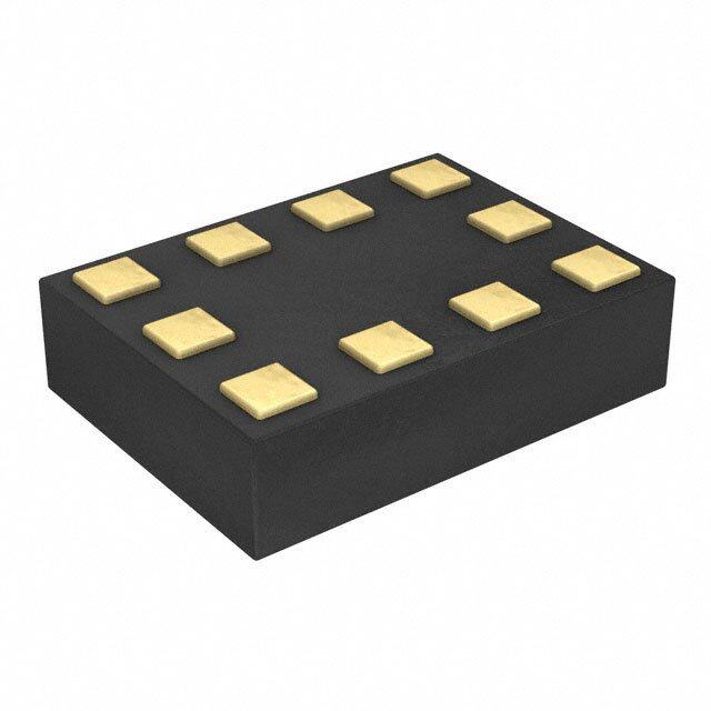
| 产品图片 |
|
| P1dB | - |
| 产品型号 | PE42520MLBA-Z |
| RF类型 | ATE |
| rohs | 无铅 / 符合限制有害物质指令(RoHS)规范要求 |
| 产品系列 | UltraCMOS®,HaRP™ |
| 供应商器件封装 | 16-QFN(3x3) |
| 其它名称 | 1046-1087-6 |
| 包装 | Digi-Reel® |
| 封装/外壳 | 16-WFQFN 裸露焊盘 |
| 工作温度 | -40°C ~ 85°C |
| 拓扑 | 吸收性 |
| 插损@频率 | 2dB @ 13GHz |
| 标准包装 | 1 |
| 特性 | - |
| 电压-电源 | 2.3 V ~ 5.5 V |
| 电路 | SPDT |
| 阻抗 | 50 欧姆 |
| 隔离@频率 | 18dB @ 13GHz (标准) |
| 频率 -上 | 13GHz |
| 频率 -下 | 9kHz |


- 商务部:美国ITC正式对集成电路等产品启动337调查
- 曝三星4nm工艺存在良率问题 高通将骁龙8 Gen1或转产台积电
- 太阳诱电将投资9.5亿元在常州建新厂生产MLCC 预计2023年完工
- 英特尔发布欧洲新工厂建设计划 深化IDM 2.0 战略
- 台积电先进制程称霸业界 有大客户加持明年业绩稳了
- 达到5530亿美元!SIA预计今年全球半导体销售额将创下新高
- 英特尔拟将自动驾驶子公司Mobileye上市 估值或超500亿美元
- 三星加码芯片和SET,合并消费电子和移动部门,撤换高东真等 CEO
- 三星电子宣布重大人事变动 还合并消费电子和移动部门
- 海关总署:前11个月进口集成电路产品价值2.52万亿元 增长14.8%


PDF Datasheet 数据手册内容提取
Product Specification PE42520 ® UltraCMOS SPDT RF Switch 9 kHz–13 GHz Product Description Features The PE42520 SPDT absorptive RF switch is designed for use in Test/ATE and other high performance wireless HaRP™ technology enhanced applications. This broadband general purpose switch maintains excellent RF performance and linearity from Fast settling time 9 kHz through 13 GHz. This switch is a pin-compatible No gate and phase lag upgraded version of PE42552 with higher power No drift in insertion loss and phase handling of 36 dBm continuous wave (CW) and 38 dBm instantaneous power in 50Ω @ 8 GHz. The PE42520 High power handling @ 8 GHz in 50Ω exhibits high isolation, fast settling time, and is offered in 36 dBm CW a 3 × 3 mm QFN package. 38 dBm instantaneous power The PE42520 is manufactured on pSemi’s UltraCMOS® 26 dBm terminated port process, a patented variation of silicon-on-insulator (SOI) High linearity technology on a sapphire substrate, offering the 66 dBm IIP3 performance of GaAs with the economy and integration of conventional CMOS. Low insertion loss 0.8 dB @ 3 GHz 0.9 dB @ 10 GHz 2.0 dB @ 13 GHz Figure 1. Functional Diagram High isolation RFC 45 dB @ 3 GHz 31 dB @ 10 GHz ES 18 dB @ 13 GHz D ESD performance RF1 RF2 4 kV HBM on RF pins to GND ESD ESD 2.5 kV HBM on all pins 1 kV CDM on all pins 50Ω 50Ω CMOS Control Driver and ESD Figure 2. Package Type - 16 lead 3 × 3 mm QFN LS CTRL Vss EXT DOC-50572 Document No. DOC-73010-2 | www.psemi.com ©2015, 2018 pSemi Corp. All rights reserved. Page 1 of 16
PE42520 Product Specification Table 1. Electrical Specifications @ +25 °C, V = 3.3V, V = 0V or V = 3.4V, V = –3.4V, DD SS_EXT DD SS_EXT (Z = Z = 50Ω), unless otherwise noted S L Parameter Path Condition Min Typ Max Unit Operation frequency 9 kHz 13 GHz shAosw n 9 kHz–10 MHz 0.60 0.80 dB 10 MHz–3 GHz 0.80 1.00 dB Insertion loss RFC–RFX 37 .G5 HGzH–z7–.51 0G GHHz z 00..8950 11..0150 ddBB 10 GHz–12 GHz 1.20 1.65 dB 12 GHz–13 GHz 2.00 2.70 dB 9 kHz–10 MHz 70 90 dB 10 MHz–3 GHz 46 54 dB Isolation RFX–RFX 37 .G5 HGzH–z7–.51 0G GHHz z 3254 3287 ddBB 10 GHz–12 GHz 16 19 dB 12 GHz–13 GHz 13 17 dB 9 kHz–10 MHz 80 90 dB 10 MHz–3 GHz 42 45 dB Isolation RFC–RFX 37 .G5 HGzH–z7–.51 0G GHHz z 4216 4341 ddBB 10 GHz–12 GHz 16 20 dB 12 GHz–13 GHz 13 18 dB 9 kHz–10 MHz 23 dB 10 MHz–3 GHz 17 dB Return loss (active port) RFC–RFX 37 .G5 HGzH–z7–.51 0G GHHz z 1158 ddBB 10 GHz–12 GHz 20 dB 12 GHz–13 GHz 10 dB 9 kHz–10 MHz 23 dB 10 MHz–3 GHz 17 dB Return loss (common port) RFC–RFX 37 .G5 HGzH–z7–.51 0G GHHz z 1158 ddBB 10 GHz–12 GHz 18 dB 12 GHz–13 GHz 10 dB 9 kHz–10 MHz 32 dB 10 MHz–3 GHz 24 dB Return loss (terminated port) RFX 37 .G5 HGzH–z7–.51 0G GHHz z 2113 ddBB 10 GHz–12 GHz 8 dB 12 GHz–13 GHz 5 dB Input 0.1dB compression point1 RFC–RFX 10 MHz–13 GHz Fig. 5 dBm Input IP2 RFC–RFX 834 MHz, 1950 MHz 120 dBm Input IP3 RFC–RFX 834 MHz, 1950 MHz, and 2700 MHz 66 dBm Settling time 50% CTRL to 0.05 dB final value 15 20 μs Switching time 50% CTRL to 90% or 10% of final value 5.5 9.5 μs Note 1: The input 0.1dB compression point is a linearity figure of merit. Refer to Table 3 for the RF input power PIN (50Ω) ©2015, 2018 pSemi Corp. All rights reserved. Document No. DOC-73010-2 | UltraCMOS® RFIC Solutions Page 2 of 16
PE42520 Product Specification Figure 3. Pin Configuration (Top View) Table 3. Operating Ranges L XT Parameter Symbol Min Typ Max Unit R E Pmianr k1i ndgot VDD LS CT Vss Smuopdpel,y VvSoSl_tEaXgT e= (0nVo)r1m al VDD 2.3 5.5 V 6 5 4 3 1 1 1 1 Supply voltage (bypass mode, VSS_EXT = –3.4V, V 2.7 3.4 5.5 V V ≥ 3.4V for full spec. DD GND 1 12 GND coDmDpliance)2 RF1 2 Exposed Pad 11 RF2 N(beygpaatsivse m soudpep)ly2 voltage VSS_EXT –3.6 –3.2 V GND 3 10 GND Smuopdpel,y VcSuSr_EreXTn =t (0nVo)r1m al IDD 120 200 µA GND 4 9 GND Smuopdpel,y VcSuSr_EreXTn =t (–b3y.p4aVs)s2 IDD 50 80 µA 5 6 7 8 Negative supply current ND ND FC ND (–b3y.p4aVs)2s mode, VSS_EXT = ISS –40 –16 µA G G R G D(CigTiRtaLl )i nput high VIH 1.17 3.6 V Table 2. Pin Descriptions Digital input low (CTRL) V –0.3 0.6 V IL Pin # Pin Name Description Digital input current I 10 µA CTRL 2 RF11 RF port 1 RF input power, CW 1, 3, 4, 5, (RFC–RFX)3 6, 8, 9, 10, GND Ground 9 kHz ≤ 10 MHz PIN_CW Fig. 4 dBm 12 10 MHz ≤ 8 GHz 36 dBm 8 GHz ≤ 13 GHz Fig. 5 dBm 7 RFC1 RF common RF input power, pulsed 1113 VRSSF_E2X1T 2 RExFt epronrat l2 V SS negative voltage control (RFC–1R09F M XkHH)4zz ≤≤ 1103 MGHHzz PIN_PULSED FFiigg .. 45 ddBB mm 14 CTRL Digital control logic input RF input power, hot 15 LS Ldoegfinici tSioenl efocrt t–h eu sCeTd RtoL dpeinte (rsmeien eT athbele 5) switch, 9C WkH3z ≤ 300 kHz PIN_HOT Fig . 4 dB m 300 kHz ≤ 13 GHz 20 dBm 16 V Supply voltage DD RF input power into Pad GND Exposed pad: ground for proper operation terminated ports, CW Notes: 1. RF pins 2, 7 and 11 must be at 0 VDC. The RF pins do not require (RFX)3 9 kHz ≤ 600 kHz PIN_TERM Fig . 4 dB m DisC m belto. cking capacitors for proper operation if the 0 VDC requirement 600 kHz ≤ 13 GHz 26 dBm 2. Use VSS_EXT (pin 13) to bypass and disable internal negative voltage ginetenrenraalt onre. gCaotinvnee vcot lVtaSgSe_E gXTe n(peirna t1o3r). to GND (VSS_EXT = 0V) to enable Orapnegrea ting temperature TOP –40 +25 +85 °C Notes: 1e.n Nabolrem inatl emrnoadl en: ecgoantniveec tv oVlStaS_gEeX Tg (epnine r1a3to) rt.o GND (VSS_EXT = 0V) to 2n.e Bgaytpivaes sv omltoadgee: guesnee VraStSo_rE.X T (pin 13) to bypass and disable internal 3. 100% duty cycle, all bands, 50Ω. 4. Pulsed, 5% duty cycle of 4620 µs period, 50Ω. Document No. DOC-73010-2 | www.psemi.com ©2015, 2018 pSemi Corp. All rights reserved. Page 3 of 16
PE42520 Product Specification Table 4. Absolute Maximum Ratings Switching Frequency Parameter/Condition Symbol Min Max Unit The PE42520 has a maximum 25 kHz switching Supply voltage VDD –0.3 5.5 V rate when the internal negative voltage generator is used (pin 13 = GND). The rate at which the Digital input voltage (CTRL) V –0.3 3.6 V CTRL PE42520 can be switched is only limited to the LS input voltage VLS –0.3 3.6 V switching time (Table 1) if an external negative RF input power, CW supply is provided (pin 13 = VSS_EXT). (RFC–RFX)1 9 kHz ≤ 10 MHz PIN_CW Fig. 4 dBm Switching frequency describes the time duration 10 MHz ≤ 8 GHz 36 dBm 8 GHz ≤ 13 GHz Fig. 5 dBm between switching events. Switching time is the time duration between the point the control signal RF input power, pulsed (RFC–RFX)2 9 kHz ≤ 10 MHz PIN_PULSED Fig . 4 dB m roeuatpchute ss ig5n0a%l roefa tchhee fsin wailt vhainlu 1e0 a%n do rt h9e0 %po oinf t ittsh e 10 MHz ≤ 13 GHz Fig. 5 dBm target value. RF input power into terminated ports, CW (RFX9) 1k Hz ≤ 10 MHz PIN_TERM Fig . 4 dB m Optional External Vss Control (V ) 10 MHz ≤ 13 GHz 26 dBm SS_EXT For proper operation, the V control pin must Maximum junction temperature TJ_MAX +150 °C be grounded or tied to the VSS_E vXoTltage specified in SS Storage temperature range T –65 +150 °C Table 3. When the V control pin is ST SS_EXT ESD voltage HBM3 grounded, FETs in the switch are biased with an RF pins to GND V 4000 V internal negative voltage generator. For ESD_HBM All pins 2500 V applications that require the lowest possible spur ESD voltage MM4, all pins VESD_MM 200 V performance, VSS_EXT can be applied externally to bypass the internal negative voltage generator. ESD voltage CDM5, all pins V 1000 V ESD_CDM Spurious Performance The typical spurious performance of the PE42520 Notes: 1. 100% duty cycle, all bands, 50Ω. 2. Pulsed, 5% duty cycle of 4620 µs period, 50Ω. is –152 dBm when VSS_EXT = 0V (pin 13 = GND). If 3. Human Body Model (MIL-STD 883 Method 3015). further improvement is desired, the internal 4. Machine Model (JEDEC JESD22-A115). 5. Charged Device Model (JEDEC JESD22-C101). negative voltage generator can be disabled by setting V = –3.4V. SS_EXT Exceeding absolute maximum ratings may cause permanent damage. Operation should be Table 5. Control Logic Truth Table restricted to the limits in the Operating Ranges table. Operation between operating range LS CTRL RFC–RF1 RFC–RF2 maximum and absolute maximum for extended 0 0 off on periods may reduce reliability. 0 1 on off 1 0 on off Electrostatic Discharge (ESD) Precautions 1 1 off on When handling this UltraCMOS device, observe the same precautions that you would use with - Moisture Sensitivity Level other ESD sensitive devices. Although this device contains circuitry to protect it from damage due to The Moisture Sensitivity Level rating for the ESD, precautions should be taken to avoid - PE42520 in the 16 lead 3 × 3 mm QFN package exceeding the rating specified. is MSL3. - Latch up Avoidance Logic Select (LS) Unlike conventional CMOS devices, UltraCMOS The Logic Select feature is used to determine the - devices are immune to latch up. definition for the CTRL pin. ©2015, 2018 pSemi Corp. All rights reserved. Document No. DOC-73010-2 | UltraCMOS® RFIC Solutions Page 4 of 16
PE42520 Product Specification Thermal Data Psi-JT ( ), junction top-of-package, is a JT thermal metric to estimate junction temperature of a device on the customer application PCB - (JEDEC JESD51 2). = (T – T )/P JT J T where = junction-to-top of package characterization JT parameter, °C/W T = die junction temperature, °C J T = package temperature (top surface, in the T center), °C P = power dissipated by device, Watts Table 6. Thermal Data for PE42520 Parameter Typ Unit Ψ 51 °C/W JT Θ , junction-to-ambient thermal resistance 79 °C/W JA - Figure 4. Power De rating Curve for 9 kHz–10 MHz (50Ω) 40 35 30 Max. RF Input Power, CW and Pulsed, (-40°C to +85°C Ambient) 25 m) B d20 er ( w o ut P15 p n I 10 5 0 -5 1 10 100 1000 10000 Frequency (kHz) Document No. DOC-73010-2 | www.psemi.com ©2015, 2018 pSemi Corp. All rights reserved. Page 5 of 16
PE42520 Product Specification - Figure 5a. Power De rating Curve for 10 MHz–13 GHz @ +25 °C Ambient (50Ω) 40 P0.1dB Compression @ 25°C Ambient 39.5 39 Max. RF Input Power, Pulsed @ 25°C Ambient 38.5 Max. RF Input Power, CW @ 25°C Ambient 38 37.5 m) B 37 d wer (36.5 o P ut 36 p n I 35.5 35 34.5 34 33.5 33 00.01 1 2 3 4 5 6 7 8 9 10 11 12 13 Frequency (GHz) - Figure 5b. Power De rating Curve for 10 MHz–13 GHz @ +85 °C Ambient (50Ω) 40 P0.1dB Compression @ 85°C Ambient 39.5 39 Max. RF Input Power, Pulsed @ 85°C Ambient 38.5 Max. RF Input Power, CW @ 85°C Ambient 38 37.5 Bm) 37 d wer (36.5 o P put 36 n I 35.5 35 34.5 34 33.5 33 00.01 1 2 3 4 5 6 7 8 9 10 11 12 13 Frequency (GHz) ©2015, 2018 pSemi Corp. All rights reserved. Document No. DOC-73010-2 | UltraCMOS® RFIC Solutions Page 6 of 16
PE42520 Product Specification Typical Performance Data @ +25 °C and V = 3.4V, unless otherwise specified DD Figure 6. Insertion Loss vs. Temp (RFC–RF1) Figure 7. Insertion Loss vs. V (RFC–RF1) DD Figure 8. Insertion Loss vs. Temp (RFC–RF2) Figure 9. Insertion Loss vs. V (RFC–RF2) DD Document No. DOC-73010-2 | www.psemi.com ©2015, 2018 pSemi Corp. All rights reserved. Page 7 of 16
PE42520 Product Specification Typical Performance Data @ +25 °C and V = 3.4V, unless otherwise specified (Cont.) DD Figure 10. RFC Port Return Loss vs. Temp Figure 11. RFC Port Return Loss vs. V DD (RF1 Active) (RF1 Active) Figure 12. RFC Port Return Loss vs. Temp Figure 13. RFC Port Return Loss vs. V DD (RF2 Active) (RF2 Active) ©2015, 2018 pSemi Corp. All rights reserved. Document No. DOC-73010-2 | UltraCMOS® RFIC Solutions Page 8 of 16
PE42520 Product Specification Typical Performance Data @ +25 °C and V = 3.4V, unless otherwise specified (Cont.) DD Figure 14. Active Port Return Loss vs. Temp Figure 15. Active Port Return Loss vs. V DD (RF1 Active) (RF1 Active) Figure 16. Active Port Return Loss vs. Temp Figure 17. Active Port Return Loss vs. V DD (RF2 Active) (RF2 Active) Document No. DOC-73010-2 | www.psemi.com ©2015, 2018 pSemi Corp. All rights reserved. Page 9 of 16
PE42520 Product Specification Typical Performance Data @ +25 °C and V = 3.4V, unless otherwise specified (Cont.) DD Figure 18. Terminated Port Return Loss vs. Temp Figure 19. Terminated Port Return Loss vs. V DD (RF1 Active) (RF1 Active) Figure 20. Terminated Port Return Loss vs. Temp Figure 21. Terminated Port Return Loss vs. V DD (RF2 Active) (RF2 Active) ©2015, 2018 pSemi Corp. All rights reserved. Document No. DOC-73010-2 | UltraCMOS® RFIC Solutions Page 10 of 16
PE42520 Product Specification Typical Performance Data @ +25 °C and V = 3.4V, unless otherwise specified (Cont.) DD Figure 22. Isolation vs. Temp Figure 23. Isolation vs. V DD (RF1–RF2, RF1 Active) (RF1–RF2, RF1 Active) Figure 24. Isolation vs. Temp Figure 25. Isolation vs. V DD (RF2–RF1, RF2 Active) (RF2–RF1, RF2 Active) Document No. DOC-73010-2 | www.psemi.com ©2015, 2018 pSemi Corp. All rights reserved. Page 11 of 16
PE42520 Product Specification Typical Performance Data @ +25 °C and V = 3.4V, unless otherwise specified (Cont.) DD Figure 26. Isolation vs. Temp Figure 27. Isolation vs. V DD (RFC–RF2, RF1 Active) (RFC–RF2, RF1 Active) Figure 28. Isolation vs. Temp Figure 29. Isolation vs. V DD (RFC–RF1, RF2 Active) (RFC–RF1, RF2 Active) ©2015, 2018 pSemi Corp. All rights reserved. Document No. DOC-73010-2 | UltraCMOS® RFIC Solutions Page 12 of 16
PE42520 Product Specification Evaluation Kit Figure 30. Evaluation Kit Layout The SPDT switch evaluation board was designed to ease customer evaluation of pSemi’s PE42520. The RF common port is connected through a 50Ω transmission line via the SMA connector, J1. RF1 and RF2 ports are connected through 50Ω transmission lines via SMA connectors J2 and J3, respectively. A 50Ω through transmission line is available via SMA connectors J5 and J6, which can be used to - de embed the loss of the PCB. J4 provides DC and digital inputs to the device. For the true performance of the PE42520 to be realized, the PCB should be designed in such a way that RF transmission lines and sensitive DC I/O traces are heavily isolated from one another. PRT-30186 Document No. DOC-73010-2 | www.psemi.com ©2015, 2018 pSemi Corp. All rights reserved. Page 13 of 16
PE42520 Product Specification Figure 31. Evaluation Board Schematic DOC-12726 Notes: 1. Use PRT-30186-02 PCB. 2. CAUTION: Contains parts and assemblies susceptible to damage by electrostatic discharge (ESD). ©2015, 2018 pSemi Corp. All rights reserved. Document No. DOC-73010-2 | UltraCMOS® RFIC Solutions Page 14 of 16
PE42520 Product Specification Figure 32. Package Drawing 0.10 C A 3.00 (2X) 0.30 0.50 B 1.70±0.05 (X16) (X12) 9 12 0.750 (X16) 0.50 (X12) 8 13 1.70±0.05 1.75 3.75 3.00 5 16 0.25±0.05 (X16) 0.10 C 4 1 (2X) 0.30±0.05 1.50 (X16) 1.75 Pin #1 Corner 3.75 TOP VIEW BOTTOM VIEW RECOMMENDED LAND PATTERN DOC-58196 0.10 C 0.10 C A B 0.85±0.05 0.05 C 0.05C ALL FEATURES SEATING PLANE 0.203 0.05 C SIDE VIEW Figure 33. Top Marking Specifications 42520 YYWW = Pin 1 designator ZZZZZZ YY = Last two digits of assembly year WW = Assembly work week ZZZZZ = Assembly lot code (maximum six characters) DOC-66052 Document No. DOC-73010-2 | www.psemi.com ©2015, 2018 pSemi Corp. All rights reserved. Page 15 of 16
PE42520 Product Specification Figure 34. Tape and Reel Specifications Direction of Feed Ao 3.30 ± 0.1 Notes: Bo 3.30 ± 0.1 1. Measured from centerline of sprocket hole to centerline of Ko 1.10 ± 0.1 Pin 1 pocket. F 5.50 ± 0.05 2. Cumulative tolerance of 10 sprocket holes ± 0.20. P1 8.00 ± 0.1 W 12.00 ± 0.3 3. Measured from centerline of sprocket hole to centerline of sprocket. Dimensions are in millimeters unless otherwise specified. Device Orientation in Tape Table 7. Ordering Information Order Code Description Package Shipping Method PE42520C-Z PE42520 SPDT RF switch Green 16-lead 3 × 3 mm QFN 3000 units / T&R PE42520MLBA-Z PE42520 SPDT RF switch Green 16-lead 3 × 3 mm QFN 3000 units / T&R EK42520-02 PE42520 Evaluation kit Evaluation kit 1 / Box EK42520-03 PE42520 Evaluation kit Evaluation kit 1 / Box Sales Contact and Information For sales and contact information please visit www.psemi.com. Advance Information: The product is in a formative or design stage. The datasheet contains design target No patent rights or licenses to any circuits described in this document are implied or granted to any third party. specifications for product development. Specifications and features may change in any manner without notice. pSemi’s products are not designed or intended for use in devices or systems intended for surgical implant, or in Preliminary Specification: The datasheet contains preliminary data. Additional data may be added at a later other applications intended to support or sustain life, or in any application in which the failure of the pSemi date. pSemi reserves the right to change specifications at any time without notice in order to supply the best product could create a situation in which personal injury or death might occur. pSemi assumes no liability for possible product. Product Specification: The datasheet contains final data. In the event pSemi decides to damages, including consequential or incidental damages, arising out of the use of its products in such change the specifications, pSemi will notify customers of the intended changes by issuing a CNF (Customer applications. Notification Form). The Peregrine Semiconductor name, Peregrine Semiconductor logo and UltraCMOS are registered trademarks The information in this document is believed to be reliable. However, pSemi assumes no liability for the use of and the pSemi name, pSemi logo, HaRP and DuNE are trademarks of pSemi Corporation in the U.S. and other this information. Use shall be entirely at the user’s own risk. countries. pSemi products are protected under one or more of the following U.S. patents: patents.psemi.com. ©2015, 2018 pSemi Corp. All rights reserved. Document No. DOC-73010-2 | UltraCMOS® RFIC Solutions Page 16 of 16