ICGOO在线商城 > 射频/IF 和 RFID > RF 开关 > SKY14151-350LF

 Datasheet下载
- 型号: SKY14151-350LF
- 制造商: SKYWORKS
- 库位|库存: xxxx|xxxx
- 要求:
| 数量阶梯 | 香港交货 | 国内含税 |
| +xxxx | $xxxx | ¥xxxx |
查看当月历史价格
查看今年历史价格
SKY14151-350LF产品简介:
ICGOO电子元器件商城为您提供SKY14151-350LF由SKYWORKS设计生产,在icgoo商城现货销售,并且可以通过原厂、代理商等渠道进行代购。 SKY14151-350LF价格参考。SKYWORKSSKY14151-350LF封装/规格:RF 开关, 射频开关 IC 手机,GSM,EDGE,WCDMA SP4T 2.5GHz 50 欧姆 16-QFN(3x3)。您可以下载SKY14151-350LF参考资料、Datasheet数据手册功能说明书,资料中有SKY14151-350LF 详细功能的应用电路图电压和使用方法及教程。
Skyworks Solutions Inc.的SKY14151-350LF是一款高性能RF(射频)开关,广泛应用于各种无线通信设备和系统中。这款器件的主要应用场景包括但不限于以下几类:

1. 智能手机和平板电脑:SKY14151-350LF能够支持多种通信标准,如LTE、WCDMA、GSM等,适用于多模多频段的移动设备。它可以在不同的频段之间快速切换,确保信号传输的稳定性和高效性。

2. 物联网(IoT)设备:在智能家居、智能城市和工业物联网等领域,该RF开关可以用于连接传感器、网关和其他低功耗无线设备,提供可靠的射频信号路径管理。

3. Wi-Fi模块和路由器:SKY14151-350LF适用于2.4GHz和5GHz频段的Wi-Fi设备,能够提高数据传输速率并减少干扰,增强网络性能。

4. 无线基础设施:在基站、小基站(Small Cell)和其他无线接入点中,这款RF开关可以实现天线分集、MIMO(多输入多输出)等功能,提升系统的覆盖范围和容量。

5. 汽车电子:随着车联网技术的发展,SKY14151-350LF也被用于车载通信模块中,支持V2X(车对万物)通信,保障车辆与外界的信息交互安全可靠。

6. 可穿戴设备:如智能手表、健康监测器等,这些设备通常需要集成多个无线通信功能,SKY14151-350LF可以帮助优化射频前端设计,延长电池寿命。

7. 军事和航空航天:对于要求高可靠性和严苛环境适应性的应用,例如卫星通信、雷达系统等,SKY14151-350LF也能发挥重要作用。

总之,SKY14151-350LF凭借其卓越的电气特性、小巧的封装尺寸以及广泛的频率覆盖范围,成为众多射频应用的理想选择。
| 参数 | 数值 |
| 产品目录 | |
| 描述 | IC SP4T 100MHZ-2.5GHZ 16QFNRF 开关 IC 20MHz-2.5GHz SP4T IL .45dB @ 2.0GHz |
| 产品分类 | |
| IIP3 | - |
| 品牌 | Skyworks Solutions Inc |
| 产品手册 | |
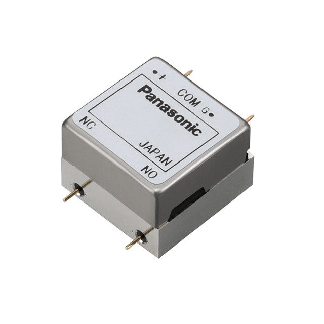
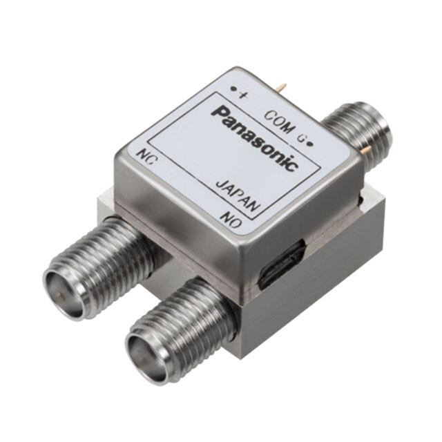
| 产品图片 |
|
| rohs | 符合RoHS无铅 / 符合限制有害物质指令(RoHS)规范要求 |
| 产品系列 | RF集成电路,RF 开关 IC,Skyworks Solutions, Inc. SKY14151-350LF- |
| 数据手册 | |
| P1dB | - |
| 产品型号 | SKY14151-350LF |
| RF类型 | 手机,GSM,EDGE,WCDMA |
| 产品目录页面 | |
| 产品种类 | RF 开关 IC |
| 介入损耗 | 0.5 dB |
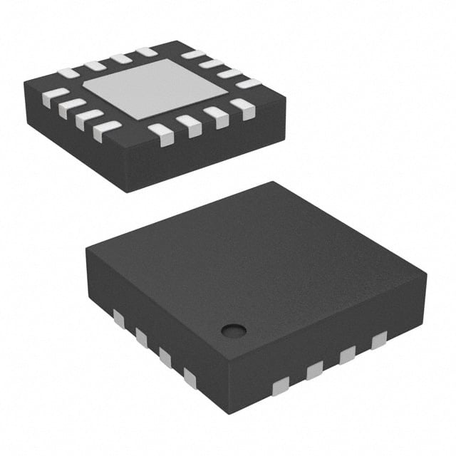
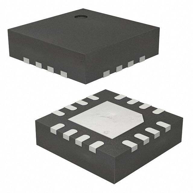
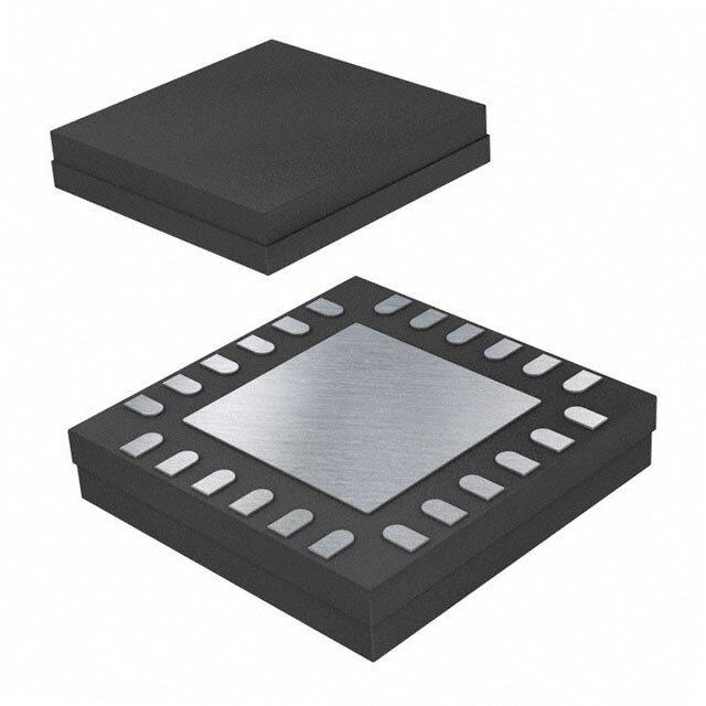
| 供应商器件封装 | 16-QFN(3x3) |
| 关闭隔离—典型值 | 23 dB |
| 其它名称 | 863-1181-6 |
| 包装 | Digi-Reel® |
| 商标 | Skyworks Solutions, Inc. |
| 安装风格 | SMD/SMT |
| 封装 | Reel |
| 封装/外壳 | 16-WFQFN 裸露焊盘 |
| 封装/箱体 | QFN-16 |
| 工作温度 | -40°C ~ 85°C |
| 工厂包装数量 | 3000 |
| 开关数量 | Single |
| 开关配置 | SP4T |
| 拓扑 | 反射 |
| 插损@频率 | 0.5dB @ 2.1GHz |
| 最大工作温度 | + 85 C |
| 最小工作温度 | - 40 C |
| 标准包装 | 1 |
| 特性 | - |
| 特色产品 | http://www.digikey.com/cn/zh/ph/Skyworks/switches.html |
| 电压-电源 | 1.8 V ~ 3 V |
| 电路 | SP4T |
| 阻抗 | 50 欧姆 |
| 隔离@频率 | 23dB @ 2.1GHz |
| 频率 | 20 MHz to 2.5 GHz |
| 频率 -上 | 2.5GHz |
| 频率 -下 | 20MHz |
| 高控制电压 | 2.65 V |


- 商务部:美国ITC正式对集成电路等产品启动337调查
- 曝三星4nm工艺存在良率问题 高通将骁龙8 Gen1或转产台积电
- 太阳诱电将投资9.5亿元在常州建新厂生产MLCC 预计2023年完工
- 英特尔发布欧洲新工厂建设计划 深化IDM 2.0 战略
- 台积电先进制程称霸业界 有大客户加持明年业绩稳了
- 达到5530亿美元!SIA预计今年全球半导体销售额将创下新高
- 英特尔拟将自动驾驶子公司Mobileye上市 估值或超500亿美元
- 三星加码芯片和SET,合并消费电子和移动部门,撤换高东真等 CEO
- 三星电子宣布重大人事变动 还合并消费电子和移动部门
- 海关总署:前11个月进口集成电路产品价值2.52万亿元 增长14.8%

PDF Datasheet 数据手册内容提取
DATA SHEET SKY14151-350LF: 20 MHz-2.5 GHz High Power SP4T Switch With Decoder Applications RF1 GSM/WCDMA/EDGE datacards and handsets Mobile high power switching systems RF2 ANT RF3 Features RF4 Broadband frequency range: 20 MHz to 2.5 GHz Low insertion loss: 0.40 dB @ 1 GHz, 0.45 dB @ 2 GHz with CTRL1 CTRL2 high isolation (29 dB @ 1 GHz) S1947 VDD: 2.5 to 3.0 V for high power applications; can be used down Figure 1. SKY14151-350LF Block Diagram to 1.8 V for low power applications High linearity IMD < –111 dBm over phase Description Good harmonic performance < –80 dBc @ 0.9 GHz The SKY14151-350LF is a symmetrical, single-pole, four-throw Low voltage logic compatible (minimum VHIGH = 1.8 V) (SP4T) switch. The device is designed for broadband, high power Small, QFN (16-pin, 3 x 3 mm) package (MSL1, 260 C per switching applications that demand high linearity and low JEDEC J-STD-020) insertion loss. This is a general purpose switch optimized for a variety of multimode applications such as GSM/WCDMA/EDGE. The switch is manufactured using Skyworks state-of-the-art pHEMT process. The SKY14151-350LF features integrated logic that uses only two control lines for switch operation. The low current consumption makes the device suitable for battery- operated applications. The SKY14151-350LF SP4T switch is provided in a compact Quad Flat No-Lead (QFN) 3 x 3 mm package. A functional block diagram is shown in Figure 1. The pin configuration and package are shown in Figure 2. Signal pin assignments and functional pin descriptions are provided in Table 1. N/C RF2 GND RF1 16 15 14 13 GND 1 12 GND VDD 2 11 ANT CTRL2 3 10 GND CTRL1 4 9 GND 5 6 7 8 D 4 D 3 GN RF GN RF S1948 Figure 2. SKY14151-350LF Pinout – 16-Pin QFN (Top View) Skyworks Solutions, Inc. • Phone [781] 376-3000 • Fax [781] 376-3100 • sales@skyworksinc.com • www.skyworksinc.com 200983H • Skyworks Proprietary Information • Products and Product Information are Subject to Change Without Notice • October 6, 2010 1
DATA SHEET • SKY14151-350LF SP4T SWITCH Table 1. SKY14151-350LF Signal Descriptions Pin # Name Description Pin # Name Description 1 GND Ground 9 GND Ground 2 VDD Supply voltage input. The voltage may be 10 GND Ground switched. The switching time must be no longer than the start-up time. 3 CTRL2 Control signal 2. The logic level applied to this 11 ANT Antenna. This pin is connected directly and pin, along with the logic level applied to pin 4, exclusively to pin 6, 8, 13, or 15 depending on controls the state of the switch. the control voltage applied to pins 3 and 4. A DC blocking capacitor is required. 4 CTRL1 Control signal 1. The logic level applied to this 12 GND Ground pin, along with the logic level applied to pin 3, controls the state of the switch. 5 GND Ground 13 RF1 RF output 1. This pin is either connected directly to or is disconnected from pin 11, depending on the control voltage applied to pins 3 and 4. A DC blocking capacitor is required. 6 RF4 RF output 4. This pin is either connected directly 14 GND Ground to or is disconnected from pin 11, depending on the control voltage applied to pins 3 and 4. A DC blocking capacitor is required. 7 GND Ground 15 RF2 RF output 2. This pin is either connected directly to or is disconnected from pin 11, depending on the control voltage applied to pins 3 and 4. A DC blocking capacitor is required. 8 RF3 RF output 3. This pin is either connected directly 16 N/C No connection. to or is disconnected from pin 11, depending on the control voltage applied to pins 3 and 4. A DC blocking capacitor is required. Table 2. SKY14151-350LF Absolute Maximum Ratings Parameter Symbol Minimum Maximum Units Supply voltage VDD 3 V Input power (20 MHz to 2.5 GHz, PIN +36 dBm VDD = 2.5 to 3.0 V) Control voltage CTRL1, CTRL2 3 V Operating temperature TOP –40 +85 C Storage temperature TSTG –50 +100 C Note: Exposure to maximum rating conditions for extended periods may reduce device reliability. There is no damage to device with only one parameter set at the limit and all other parameters set at or below their nominal value. Exceeding any of the limits listed here may result in permanent damage to the device. CAUTION: Although this device is designed to be as robust as possible, Electrostatic Discharge (ESD) can damage this device. This device must be protected at all times from ESD. Static charges may easily produce potentials of several kilovolts on the human body or equipment, which can discharge without detection. Industry-standard ESD precautions should be used at all times. Skyworks Solutions, Inc. • Phone [781] 376-3000 • Fax [781] 376-3100 • sales@skyworksinc.com • www.skyworksinc.com 2 October 6, 2010 • Skyworks Proprietary Information • Products and Product Information are Subject to Change Without Notice • 200983H
DATA SHEET • SKY14151-350LF SP4T SWITCH Functional Description When VDD is not applied, the device is considered off or inactive. All arms of the switch remain on in this state, creating a poor The SKY14151-350LF is comprised of a CMOS decoder that four-way power splitter. The return loss of all RF ports is very low enables two TTL-compatible DC lines to control four RF ports. The decoder is internally connected to a GaAs pHEMT RF switch. in this state. RF should not be applied when VDD is not present and should only be used to conserve current. Depending on the logic voltage level applied to the control pins, the ANT pin is connected to one of four switched RF outputs (RF1, RF2, RF3, or RF4) by a low insertion loss path, while maintaining Electrical and Mechanical Specifications a high isolation path to the alternate port. The absolute maximum ratings of the SKY14151-350LF are Startup time is defined as the time from when VDD is applied to provided in Table 2. Electrical specifications are provided in when the switch is active. Once the startup time has passed, the Table 3. control voltages CTRL1 and CTRL2 can be applied. RF power should not be applied during the startup time or damage to the The state of the SKY14151-350LF is determined by the logic device could result. provided in Table 4. The recommended startup sequence is: Typical performance characteristics of the SKY14151-350LF are illustrated in Figures 3 through 10. Step 1: Apply VDD. Figure 11 illustrates the test setup used to measure data for 3rd Step 2: Apply CTRL1 and CTRL2 Order Intermodulation Distortion (IMD3) testing. Figure 12 Step 3: Apply RF input. illustrates the test setup used to measure triple beat ratio data. The device must be turned off in the reverse order. Table 3. SKY14151-350LF Electrical Specifications (1 of 3) (Note 1) (VDD = 2.65 V, CTRL1 = CTRL2 = VDD, TOP = +25 C, All Unused RF Ports are Terminated in a 50 Ω Load, Unless Otherwise Noted) Parameter Symbol Test Condition Min Typical Max Units RF Specifications Insertion loss IL 0.02 to 1.0 GHz 0.40 0.50 dB 1.0 to 2.0 GHz 0.45 0.60 dB 2.0 to 2.1 GHz 0.50 0.60 dB Isolation ISO 0.02 to 1.0 GHz 26 29 dB 1.0 to 2.0 GHz 19 24 dB 2.0 to 2.1 GHz 19 23 dB Return loss |S11| 0.02 to 2.5 GHz, all RF 15 dB ports, insertion loss state Second harmonic 2fo fFUND = 900 MHz, PIN = +34.5 dBm –75 –80 dBc fFUND = 0.12 GHz, PIN = +10 dBm –75 –80 dBc fFUND = 0.4 GHz, PIN = +10 dBm –80 –90 dBc fFUND = 1.8 GHz, PIN = +31.5 dBm –70 –85 dBc Third harmonic 3fo fFUND = 900 MHz, PIN = +34.5 dBm –70 –80 dBc fFUND = 0.12 GHz, PIN = +10 dBm –80 –90 dBc fFUND = 0.4 GHz, PIN = +10 dBm –80 –90 dBc fFUND = 1.8 GHz, PIN = +31.5 dBm –70 –80 dBc Skyworks Solutions, Inc. • Phone [781] 376-3000 • Fax [781] 376-3100 • sales@skyworksinc.com • www.skyworksinc.com 200983H • Skyworks Proprietary Information • Products and Product Information are Subject to Change Without Notice • October 6, 2010 3
DATA SHEET • SKY14151-350LF SP4T SWITCH Table 3. SKY14151-350LF Electrical Specifications (2 of 3) (Note 1) (VDD = 2.65 V, CTRL1 = CTRL2 = VDD, TOP = +25 C, All Unused RF Ports are Terminated in a 50 Ω Load, Unless Otherwise Noted) Parameter Symbol Test Condition Min Typical Max Units RF Specifications (continued) Input 0.1 dB compression point P0.1dB @ 48 MHz +38.5 dBm @ 900 MHz +37.0 +38.0 dBm @ 1.8 GHz +34.0 +35.0 dBm 3rd Order Intermodulation Distortion IMD3 fFUND = 1.95 GHz @ –111 dBm +20 dBm, fBLK = 1.76 GHz @ –15 dBm, fRX = 2.14 GHz, worst case over phase. See Figure 9. Power handling under mismatch @ 900 MHz, VSWR = 20:1 +34.5 dBm @ 1.8 GHz, VSWR = 20:1 +31.5 dBm 2nd Order Input Intercept Point IIP2 f0 = 836.61 MHz +113.5 dBm @ +26 dBm, f2 = 1718.22 MHz @ –20 dBm, measured @ 881.61 MHz Switching speed 10/90% RF rise/fall time 5 μs Startup time Wait time required from 25 μs when VDD is applied until control voltage can be applied Triple beat ratio (matched) 3BR f1 = 1880 MHz, +81 +82 dBc P1 = +21.5 dBm, f2 = 1881 MHz, P2 = +21.5 dBm, fJAMMER = 1960 MHz, PJAMMER = –30 dBm, measured @ 1959 MHz and 1961 MHz for worst case, 50 Ω load f1 = 891.025 MHz +81 +82 dBc @ +14 dBm, f2 = 892.025 MHz, P2 = +14 dBm, fJAMMER = 836.0125 MHz, PJAMMER = –30 dBm, measured @ 835.0125 MHz and 837.0125 MHz for worst case, 50 Ω load f1 = 825.995 MHz, +81 +82 dBc P1 = +21.5 dBm, f2 = 826.995 MHz, P2 = +21.5 dBm, fJAMMER = 870.995 MHz, PJAMMER = –30 dBm, measured @ 869.995 MHz and 871.995 MHz for worst case, 50 Ω load Skyworks Solutions, Inc. • Phone [781] 376-3000 • Fax [781] 376-3100 • sales@skyworksinc.com • www.skyworksinc.com 4 October 6, 2010 • Skyworks Proprietary Information • Products and Product Information are Subject to Change Without Notice • 200983H
DATA SHEET • SKY14151-350LF SP4T SWITCH Table 3. SKY14151-350LF Electrical Specifications (3 of 3) (Note 1) (VDD = 2.65 V, CTRL1 = CTRL2 = VDD, TOP = +25 C, All Unused RF Ports are Terminated in a 50 Ω Load, Unless Otherwise Noted) Parameter Symbol Test Condition Min Typical Max Units RF Specifications (continued) Triple beat ratio (2:1 VSWR) 3BR f1 = 1880 MHz, +81 +82 dBc P1 = +21.5 dBm, f2 = 1881 MHz, P2 = +21.5 dBm, fJAMMER = 1960 MHz, PJAMMER = –30 dBm, measured @ 1959 MHz and 1961 MHz for worst case over phase, 2:1 VSWR load f1 = 891.025 MHz, +81 +82 dBc P1 = +14 dBm, f2 = 892.025 MHz, P2 = +14 dBm, fJAMMER = 836.0125 MHz, PJAMMER = –30 dBm, measured @ 835.0125 MHz and 837.0125 MHz for worst case over phase, 2:1 VSWR load f1 = 825.995 MHz, +81 +82 dBc P1 = +21.5 dBm, f2 = 826.995 MHz, P2 = +21.5 dBm, fJAMMER = 870.995 MHz, PJAMMER = –30 dBm, measured @ 869.995 MHz and 871.995 MHz for worst case over phase, 2:1 VSWR load DC/Control Specifications Switched supply voltage (Note 2) VDD 1.8 2.0 3.00 V Switched supply current IDD 0.3 mA Control voltage: CTRL1, CTRL2 High 1.80 (Note 3) 2.65 3.00 V Low 0 0.3 V Control current: ICTL High 0.5 μA Low 0.5 μA Note 1: Performance is guaranteed only under the conditions listed in this Table. Note 2: For best receiver sensitivity, VDD is recommended to be between 1.8 and 2.0 V with CTRL1/2 (high) no larger than VDD. Note 3: For 1.8 V control, VDD must be ≤ 2.65 V. Skyworks Solutions, Inc. • Phone [781] 376-3000 • Fax [781] 376-3100 • sales@skyworksinc.com • www.skyworksinc.com 200983H • Skyworks Proprietary Information • Products and Product Information are Subject to Change Without Notice • October 6, 2010 5
DATA SHEET • SKY14151-350LF SP4T SWITCH Table 4. SKY14151-350LF Truth Table State CTRL1 (Pin 4) CTRL2 (Pin 3) RF Path 1 VLOW VLOW ANT to RF1 2 VLOW VHIGH ANT to RF2 3 VHIGH VLOW ANT to RF3 4 VHIGH VHIGH ANT to RF4 Note: VHIGH = 1.8 V to VDD VLOW = 0 to 0.3 V Any state other than described in this Table places the switch into an undefined state. Typical Performance Characteristics (VDD = 2.5 to 3.0 V, CTRL1 = CTRL2 = VDD, TOP = +25 C, All Unused RF Ports are Terminated in a 50 Ω Load, Unless Otherwise Noted) 0 0 ––00..21 RRRRFFFF1234 –5 AAANNNTTT tttooo RRRFFF234 –10 B) –0.3 nsertion Loss (d ––––0000....7654 Isolation (dB) –––221505 I –30 –0.8 –0.9 –35 –1.0 –40 0.5 1.0 1.5 2.0 2.5 3.0 0.5 1.0 1.5 2.0 2.5 3.0 Frequency (GHz) Frequency (GHz) Figure 3. Insertion Loss vs Frequency Figure 4. Isolation vs Frequency (ANT to RF1 Insertion Loss State) 0 0 ANT to RF1 –5 AANNTT ttoo RRFF34 –5 AANNTT ttoo RRFF12 ANT to RF4 –10 –10 Isolation (dB) –––221505 Isolation (dB) –––221505 –30 –30 –35 –35 –400.5 1.0 1.5 2.0 2.5 3.0 –40 0.5 1.0 1.5 2.0 2.5 3.0 Frequency (GHz) Frequency (GHz) Figure 5. Isolation vs Frequency Figure 6. Isolation vs Frequency (ANT to RF2 Insertion Loss State) (ANT to RF3 Insertion Loss State) Skyworks Solutions, Inc. • Phone [781] 376-3000 • Fax [781] 376-3100 • sales@skyworksinc.com • www.skyworksinc.com 6 October 6, 2010 • Skyworks Proprietary Information • Products and Product Information are Subject to Change Without Notice • 200983H
DATA SHEET • SKY14151-350LF SP4T SWITCH 0 0 ANT to RF1 RF1 –5 ANT to RF2 –5 RF2 ANT to RF3 RF3 –10 B) –10 RF4 d Isolation (dB) ––––32210505 Input Return Loss ( ––––32210505 –35 –35 –40 –40 0.5 1.0 1.5 2.0 2.5 3.0 0.5 1.0 1.5 2.0 2.5 3.0 Frequency (GHz) Frequency (GHz) Figure 7. Isolation vs Frequency Figure 8. Input Return Loss vs Frequency (ANT to RF4 Insertion Loss State) –100 +5 –105 +4 IMD3 (dBm) –––111211050 Noise Figure (dB) +++213 0 –125 –1 0.6 0.8 1.0 1.2 1.4 1.6 1.8 2.0 2.2 –130 Frequency (GHz) 0 20 40 60 80 100 120 140 160 180 Note: For best receiver sensitivity, VDD is recommended to be between 1.8 and 2.0 V Phase (deg) with CTRL1/2 (high) no larger than VDD. Figure 9. 3rd Order Intermodulation Distortion vs Phase Figure 10. Typical Noise Figure vs Frequency (VDD = 2 V, CTRL1/2 = 1.8 V) fBLK fFUND fRX 1760 MHz 1950 MHz 2140 MHz, @ –15 dBm @ +20 dBm Measure Tone Circulator Signal Generator Coupler to Monitor 1950 MHz fFUND = 1950 MHz, Input Power Bandpass Filter @ +20 dBm Circulator Duplexer Phase Shifter SPPKFBUYLNK1D 4==1 –5+1125-03 d 5dB0BmLmF Ba1nd7p6a0s Ms HFizlter SfBiLg@Kn = a–l 1 1G57e 6dn0Be rmMat Hozr Spectrum Analyzer fRX = 2140 MHz S1909a Figure 11. 3rd Order Intermodulation Test Setup Skyworks Solutions, Inc. • Phone [781] 376-3000 • Fax [781] 376-3100 • sales@skyworksinc.com • www.skyworksinc.com 200983H • Skyworks Proprietary Information • Products and Product Information are Subject to Change Without Notice • October 6, 2010 7
DATA SHEET • SKY14151-350LF SP4T SWITCH Circulator LPF Testing under mismatched conditions over phase f1 Combiner or testing under matched conditions: ZL = 50 Ω PIN1, PIN2, Circulator PINJAMMER f1, f2 Phase Shifter Directional Coupler LPF SKY14151-350LF 10 dB 10 dB f2 fJAMMER fJAMMER ZL P Spectrum Analyzer 10 dB 10 dB 30 dB Circulator f fJAMMER P3BL, P3BH Power Meter P (dBm) 3BRL = PJAMMER – P3BL PJAMMER 3BRH = PJAMMER – P3BH 3BR = Min(3BRL, 3BRH) P3BL P3BH f f3BL = fJAMMER – (f2 – f1) fJAMMER f3BH = fJAMMER + (f2 – f1) S1972 Figure 12. Triple Beat Ratio (3BR) Test Setup Evaluation Board Description Decoupling capacitors (C3 through C6) are recommended to suppress noise and to prevent RF leakage into the DC control The SKY14151-350LF Evaluation Board is used to test the circuits. performance of the SKY14151-350LF SP4T Switch. An Evaluation Board schematic diagram is provided in Figure 13. An assembly DC blocking capacitors C1, C2, C7, C8, and C9 determine the low drawing for the Evaluation Board is shown in Figure 14. frequency operation of the switch. Increase the capacitor values to lower operation frequency. Components C3 and L1 constitute an ESD filter. This topology and the component values noted in Figure 13 may vary according to the ESD requirement and acceptable insertion loss for a specific application. Skyworks Solutions, Inc. • Phone [781] 376-3000 • Fax [781] 376-3100 • sales@skyworksinc.com • www.skyworksinc.com 8 October 6, 2010 • Skyworks Proprietary Information • Products and Product Information are Subject to Change Without Notice • 200983H
DATA SHEET • SKY14151-350LF SP4T SWITCH RF Output 2 RF Output 4 C1 × C2 100 pF 16 15 14 13 100 pF C 2 D 1 N/ RF GN RF 1 GND GND 12 C3 L1 1 pF 10 nH Supply Voltage 2 VDD ANT 11 Antenna C4 10 nF C9 3 10 100 pF Control Signal 2 CTRL2 GND C5 100 pF 4 9 CTRL1 GND Control Signal 1 C6 100 pF GND RF4 GND RF3 5 6 7 8 RF Output 4 RF Output 3 C7 C8 100 pF 100 pF Note: Some component labels may be different than the corresponding component symbol shown here. Component values, however, are accurate as of the date of this Data Sheet. S1950 Use 10 nF DC blocking capacitors (C1, C2, C7, C8, and C9) for <50 MHz operation. Figure 13. SKY14151-350LF Evaluation Board Schematic V1 V2 VDD VBAT RF2 RF4 RF1 RF3 ANT S1949 Figure 14. SKY14151-350LF Evaluation Board Assembly Diagram Skyworks Solutions, Inc. • Phone [781] 376-3000 • Fax [781] 376-3100 • sales@skyworksinc.com • www.skyworksinc.com 200983H • Skyworks Proprietary Information • Products and Product Information are Subject to Change Without Notice • October 6, 2010 9
DATA SHEET • SKY14151-350LF SP4T SWITCH Package Dimensions when the part is subjected to high temperature during solder assembly. The PCB layout footprint for the SKY14151-350LF is provided in Figure 15. Typical case markings are shown in Figure 16. THE SKY14151-350LF is rated to Moisture Sensitivity Level 1 Package dimensions for the 16-pin QFN are shown in Figure 17, (MSL1) at 260 C. It can be used for lead or lead-free soldering. and tape and reel dimensions are provided in Figure 18. Care must be taken when attaching this product, whether it is done manually or in a production solder reflow environment. Production quantities of this product are shipped in a standard Package and Handling Information tape and reel format. Instructions on the shipping container label regarding exposure to moisture after the container seal is broken must be followed. Otherwise, problems related to moisture absorption may occur 16X 1.10 0.225 X 45o 0.25 1.70 12X 0.50 Pitch 4x Plated Through Vias See Detail A Metal Ground Pad 1.70 0.25 Exposed Soldering Area 0.60 Detail A All dimensions are in millimeters S1691 Figure 15. SKY14151-350LF PCB Layout Footprint (Top View) Skyworks Solutions, Inc. • Phone [781] 376-3000 • Fax [781] 376-3100 • sales@skyworksinc.com • www.skyworksinc.com 10 October 6, 2010 • Skyworks Proprietary Information • Products and Product Information are Subject to Change Without Notice • 200983H
DATA SHEET • SKY14151-350LF SP4T SWITCH Pin 1 Indicator Skyworks Part # Lot # Date Code: (Y = Calendar Year WW = Week) Figure 16. Typical Case Markings (Top View) –C– 1.70 +0.10/–0.15 3.00 –A– (S0e.a2t0in)g Plane –A– Exposed Pad 0.85 O.225 x 45o Pin 1 –B– 0.02 + 0.03/–0.02 Pin 1 Indicator Indicator 0.85 –B– 3.00 1.70 +0.10/–0.15 2X 0.15 C Detail B 16X 2 0.08 C 2X 0.15 C 0.75 ± 0.05 Detail A 0.10C Top View Side View Bottom View 0.40 ± 0.10 0.5 0.25 0.25 +0.05/–0.07 0.10 M C A B 0.05 M C Detail A Detail B Scale: 20X Scale: 10X 16 Places All measurements are in millimeters. Dimensioning and tolerancing according to ASME Y14.5M-1994. Coplanarity applies to the exposed heat sink slug as well as the terminals.. Plating requirement per source control drawing (SCD) 2504. S1692 Figure 17. SKY14151-350LF 16-Pin QFN Package Dimensions Skyworks Solutions, Inc. • Phone [781] 376-3000 • Fax [781] 376-3100 • sales@skyworksinc.com • www.skyworksinc.com 200983H • Skyworks Proprietary Information • Products and Product Information are Subject to Change Without Notice • October 6, 2010 11
DATA SHEET • SKY14151-350LF SP4T SWITCH 4.00 ± 0.10 ∅1.50 + 0.1/–0.0 0.30 ± 0.05 (T) Pin #1 8.00 ± 0.10 2.00 ± 0.05 B 1.75 ± 0.10 5 0 0. 0 ± 0.10 (Bo) A A 5.50 ± 12.00 ± 0.3 0 3 3. B 1.10 ± 0.10 (Ko) R0.25 Typ. ∅1.50 Min. B 3.30 ± 0.10 (Ao) A Notes: 1. Carrier tape: black conductive polystyrene, non-bakeable material. 2. Cover tape material: transparent conductive HSA. 3. Cover tape size: 9.20 mm width. 4. All measurements are in millimeters. S1698 Figure 18. SKY14151-350LF Tape and Reel Dimensions Skyworks Solutions, Inc. • Phone [781] 376-3000 • Fax [781] 376-3100 • sales@skyworksinc.com • www.skyworksinc.com 12 October 6, 2010 • Skyworks Proprietary Information • Products and Product Information are Subject to Change Without Notice • 200983H
DATA SHEET • SKY14151-350LF SP4T SWITCH Ordering Information Model Name Manufacturing Part Number Evaluation Board Part Number SKY14151-350LF SP4T Switch SKY14151-350LF SKY14151-350LF-EVB Copyright © 2008, 2009, 2010 Skyworks Solutions, Inc. All Rights Reserved. Information in this document is provided in connection with Skyworks Solutions, Inc. (“Skyworks”) products or services. These materials, including the information contained herein, are provided by Skyworks as a service to its customers and may be used for informational purposes only by the customer. Skyworks assumes no responsibility for errors or omissions in these materials or the information contained herein. Skyworks may change its documentation, products, services, specifications or product descriptions at any time, without notice. Skyworks makes no commitment to update the materials or information and shall have no responsibility whatsoever for conflicts, incompatibilities, or other difficulties arising from any future changes. No license, whether express, implied, by estoppel or otherwise, is granted to any intellectual property rights by this document. Skyworks assumes no liability for any materials, products or information provided hereunder, including the sale, distribution, reproduction or use of Skyworks products, information or materials, except as may be provided in Skyworks Terms and Conditions of Sale. THE MATERIALS, PRODUCTS AND INFORMATION ARE PROVIDED “AS IS” WITHOUT WARRANTY OF ANY KIND, WHETHER EXPRESS, IMPLIED, STATUTORY, OR OTHERWISE, INCLUDING FITNESS FOR A PARTICULAR PURPOSE OR USE, MERCHANTABILITY, PERFORMANCE, QUALITY OR NON-INFRINGEMENT OF ANY INTELLECTUAL PROPERTY RIGHT; ALL SUCH WARRANTIES ARE HEREBY EXPRESSLY DISCLAIMED. SKYWORKS DOES NOT WARRANT THE ACCURACY OR COMPLETENESS OF THE INFORMATION, TEXT, GRAPHICS OR OTHER ITEMS CONTAINED WITHIN THESE MATERIALS. SKYWORKS SHALL NOT BE LIABLE FOR ANY DAMAGES, INCLUDING BUT NOT LIMITED TO ANY SPECIAL, INDIRECT, INCIDENTAL, STATUTORY, OR CONSEQUENTIAL DAMAGES, INCLUDING WITHOUT LIMITATION, LOST REVENUES OR LOST PROFITS THAT MAY RESULT FROM THE USE OF THE MATERIALS OR INFORMATION, WHETHER OR NOT THE RECIPIENT OF MATERIALS HAS BEEN ADVISED OF THE POSSIBILITY OF SUCH DAMAGE. Skyworks products are not intended for use in medical, lifesaving or life-sustaining applications, or other equipment in which the failure of the Skyworks products could lead to personal injury, death, physical or environmental damage. Skyworks customers using or selling Skyworks products for use in such applications do so at their own risk and agree to fully indemnify Skyworks for any damages resulting from such improper use or sale. Customers are responsible for their products and applications using Skyworks products, which may deviate from published specifications as a result of design defects, errors, or operation of products outside of published parameters or design specifications. Customers should include design and operating safeguards to minimize these and other risks. Skyworks assumes no liability for applications assistance, customer product design, or damage to any equipment resulting from the use of Skyworks products outside of stated published specifications or parameters. Skyworks, the Skyworks symbol, and “Breakthrough Simplicity” are trademarks or registered trademarks of Skyworks Solutions, Inc., in the United States and other countries. Third-party brands and names are for identification purposes only, and are the property of their respective owners. Additional information, including relevant terms and conditions, posted at www.skyworksinc.com, are incorporated by reference. Skyworks Solutions, Inc. • Phone [781] 376-3000 • Fax [781] 376-3100 • sales@skyworksinc.com • www.skyworksinc.com 200983H • Skyworks Proprietary Information • Products and Product Information are Subject to Change Without Notice • October 6, 2010 13