ICGOO在线商城 > 射频/IF 和 RFID > RF 开关 > MA4SW210B-1
 Datasheet下载
- 型号: MA4SW210B-1
- 制造商: M/A-COM
- 库位|库存: xxxx|xxxx
- 要求:
| 数量阶梯 | 香港交货 | 国内含税 |
| +xxxx | $xxxx | ¥xxxx |
查看当月历史价格
查看今年历史价格
MA4SW210B-1产品简介:
ICGOO电子元器件商城为您提供MA4SW210B-1由M/A-COM设计生产,在icgoo商城现货销售,并且可以通过原厂、代理商等渠道进行代购。 MA4SW210B-1价格参考。M/A-COMMA4SW210B-1封装/规格:RF 开关, RF Switch IC General Purpose SPDT 18GHz Die。您可以下载MA4SW210B-1参考资料、Datasheet数据手册功能说明书,资料中有MA4SW210B-1 详细功能的应用电路图电压和使用方法及教程。
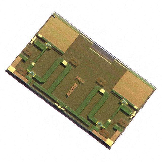
MA4SW210B-1是M/A-Com Technology Solutions公司推出的一款射频(RF)开关,属于高性能GaAs(砷化镓)单刀双掷(SPDT)开关器件。该器件广泛应用于需要高频信号切换的通信和射频系统中。

其主要应用场景包括:无线通信基础设施,如基站收发系统(BTS),用于在发射与接收路径之间快速切换;雷达系统,特别是在相控阵雷达中实现天线通道的高效切换;测试与测量设备,如矢量网络分析仪和信号发生器,用于自动切换不同测试路径以提高测量精度与效率;以及航空航天和国防领域的电子战系统、通信中继设备等,对高可靠性与宽频带性能要求较高的场合。

MA4SW210B-1工作频率范围宽(典型覆盖DC至6 GHz),具有低插入损耗、高隔离度和快速开关速度等优点,适合在紧凑型微波模块和高密度PCB设计中使用。同时,该器件采用小型表面贴装封装,便于集成到现代高频电路中。

由于其出色的射频性能和稳定性,MA4SW210B-1也适用于工业级和严苛环境下的应用,是高性能RF前端设计中的关键组件之一。
| 参数 | 数值 |
| 产品目录 | |
| 描述 | DIODE SWITCH HMIC CHIP SPDTRF 开关 IC 2-18GHz ISO 40dB IL 1.2dB @ 18GHz |
| 产品分类 | |
| IIP3 | - |
| 品牌 | MACOMM/A-Com Technology Solutions |
| 产品手册 | |
| 产品图片 |
|
| rohs | 符合RoHS无铅 / 符合限制有害物质指令(RoHS)规范要求 |
| 产品系列 | RF集成电路,RF 开关 IC,MACOM MA4SW210B-1HMIC™ |
| 数据手册 | |
| P1dB | - |
| 产品型号 | MA4SW210B-1MA4SW210B-1 |
| RF类型 | 通用 |
| 产品种类 | RF 开关 IC |
| 介入损耗 | 1.2 dB |
| 供应商器件封装 | 模具 |
| 关闭隔离—典型值 | 40 dB |
| 其它名称 | 1465-1050 |
| 包装 | 托盘 |
| 商标 | MACOM |
| 安装风格 | SMD/SMT |
| 封装 | Tray |
| 封装/外壳 | 模具 |
| 封装/箱体 | HMIC Die |
| 工作温度 | -65°C ~ 125°C |
| 工厂包装数量 | 25 |
| 开关数量 | Single |
| 开关配置 | SPDT |
| 拓扑 | 反射 |
| 插损@频率 | 1.2dB @ 18GHz |
| 最大工作温度 | + 125 C |
| 最小工作温度 | - 65 C |
| 标准包装 | 25 |
| 特性 | - |
| 电压-电源 | - |
| 电源电流 | 20 mA |
| 电路 | SPDT |
| 阻抗 | - |
| 隔离@频率 | 40dB @ 18GHz (标准) |
| 频率 | 2 GHz to 18 GHz |
| 频率 -上 | 18GHz |
| 频率 -下 | 2GHz |


- 商务部:美国ITC正式对集成电路等产品启动337调查
- 曝三星4nm工艺存在良率问题 高通将骁龙8 Gen1或转产台积电
- 太阳诱电将投资9.5亿元在常州建新厂生产MLCC 预计2023年完工
- 英特尔发布欧洲新工厂建设计划 深化IDM 2.0 战略
- 台积电先进制程称霸业界 有大客户加持明年业绩稳了
- 达到5530亿美元!SIA预计今年全球半导体销售额将创下新高
- 英特尔拟将自动驾驶子公司Mobileye上市 估值或超500亿美元
- 三星加码芯片和SET,合并消费电子和移动部门,撤换高东真等 CEO
- 三星电子宣布重大人事变动 还合并消费电子和移动部门
- 海关总署:前11个月进口集成电路产品价值2.52万亿元 增长14.8%


PDF Datasheet 数据手册内容提取
MA4SWx10B-1 Series HMIC™ Silicon PIN Diode Switches with Integrated Bias Network Rev. V6 Features Functional Diagrams1 Broad Bandwidth Specified 2 - 18 GHz Usable up to 26 GHz Integrated Bias Network MA4SW210B-1 (SP2T) Lower Insertion Loss / Higher Isolation Fully Monolithic, Glass Encapsulated Chip Up to +33 dBm CW Power Handling @ +25°C RoHS* Compliant Description The MA4SW210B-1 (SP2T) and MA4SW310B-1 (SP3T) broadband switches with an integrated bias networks utilizing MACOM’s HMICTM (Heterolithic Microwave Integrated Circuit) process, US Patent 5,268,310. This process allows the incorporation of silicon pedestals that form series and shunt diodes or vias by imbedding them in low loss, low dispersion glass. By using small spacing between circuit elements, this combination of silicon and glass gives HMIC devices low loss and high isolation performance with exceptional repeatability through low millimeter frequencies. MA4SW310B-1 (SP3T) The top side of the chip is protected by a polymer coating for manual or automatic handling and large gold bond pads help facilitate connection of low inductance ribbons. The gold metallization on the backside of the chip allows for attachment via 80/20 (gold/tin) solder or conductive silver epoxy. Ordering Information Part Number Package MA4SW210B-1 Gel Pack MA4SW310B-1 Gel Pack 1. Yellow areas indicate ribbon/wire bonding pads *Restrictions on Hazardous Substances, European Union Directive 2011/65/EU. 111 M/A-COM Technology Solutions Inc. (MACOM) and its affiliates reserve the right to make changes to the product(s) or information contained herein without notice. Visit www.macom.com for additional data sheets and product information. For further information and support please visit: https://www.macom.com/support
MA4SWx10B-1 Series HMIC™ Silicon PIN Diode Switches with Integrated Bias Network Rev. V6 Electrical Specifications: T = 25°C, 20 mA A MA4SW210B-1 (SPDT) Parameter Test Conditions Units Min. Typ. Max. 2 GHz 1.5 1.8 6 GHz 0.7 1.0 Insertion Loss dB — 12 GHz 0.9 1.2 18 GHz 1.2 1.8 2 GHz 55 60 6 GHz 47 50 Isolation dB — 12 GHz 40 45 18 GHz 36 40 2 GHz 14 6 GHz 15 Input Return Loss dB — — 12 GHz 15 18 GHz 13 Switching Speed2 — ns — 50 — MA4SW310B-1 (SP3T) Parameter Test Conditions Units Min. Typ. Max. 2 GHz 1.6 2.0 6 GHz 0.8 1.1 Insertion Loss dB — 12 GHz 1.0 1.3 18 GHz 1.3 1.9 2 GHz 54 59 6 GHz 47 50 Isolation dB — 12 GHz 40 45 18 GHz 36 40 2 GHz 14 6 GHz 15 Input Return Loss dB — — 12 GHz 16 18 GHz 14 Switching Speed2 — ns — 50 — 1. Typical switching speed is measured from (10% to 90% and 90% to 10% of detected RF voltage), driven by TTL compatible drivers. In the modulating state, (the switching port is modulating, all other ports are in steady state isolation.) The switching speed is measured using an RC network using the following values: R = 50 - 200 Ω, C = 390 - 1000 pF. Driver spike current, I = C dv/dt, ratio of spike current to steady C state current, is typically 10:1. 222 M/A-COM Technology Solutions Inc. (MACOM) and its affiliates reserve the right to make changes to the product(s) or information contained herein without notice. Visit www.macom.com for additional data sheets and product information. For further information and support please visit: https://www.macom.com/support
MA4SWx10B-1 Series HMIC™ Silicon PIN Diode Switches with Integrated Bias Network Rev. V6 Absolute Maximum Ratings3,4,5 Cleanliness The chips should be handled in a clean environment Parameter Absolute Maximum free of dust and organic contamination. RF CW Incident Power +33 dBm Wire / Ribbon Bonding Reverse Voltage -50 V Thermo compression wedge bonding using 0.003” x 0.00025” ribbon or 0.001” diameter gold wire is Bias Current per Port ±50 mA @ +25°C recommended. A work stage temperature of 150°C - 200°C, tool tip temperature of 120°C - 150° Operating Temperature -65°C to +125°C and a downward force of 18 to 22 grams should be Storage Temperature -65°C to +150°C used. If ultrasonic energy is necessary, it should be adjusted to the minimum level required to achieve a Junction Temperature +175°C good bond. Excessive power or force will fracture the silicon beneath the bond pad causing it to lift. 3. Exceeding any one or combination of these limits may cause RF bond wires and ribbons should be kept as short permanent damage to this device. 4. MACOM does not recommend sustained operation near these as possible for optimum RF performance. survivability limits. 5. Maximum operating conditions for a combination of RF power, Chip Mounting DC bias and temperature: +33 dBm CW @ 15 mA (per diode) @ +85°C. HMIC switches have Ti-Pt-Au backside metallization and can be mounted using a gold-tin eutectic solder or conductive epoxy. Mounting surface must be free of contamination and flat. Eutectic Die Attachment Handling Procedures An 80/20, gold-tin, eutectic solder is recommended. Please observe the following precautions to avoid Adjust the work surface temperature to 255oC and damage: the tool tip temperature to 265oC. After placing the chip onto the circuit board re-flow the solder by Static Sensitivity applying hot forming gas (95/5 Ni/H) to the top These electronic devices are sensitive to surface of the chip. Temperature should be electrostatic discharge (ESD) and can be damaged approximately 290oC and not exceed 320oC for by static electricity. Proper ESD control techniques more than 20 seconds. Typically no more than three should be used when handling these Class 0 seconds is necessary for attachment. Solders rich in (HBM) and Class C1 (CDM).devices. tin should be avoided Epoxy Die Attachment A minimum amount of epoxy, 1 - 2 mils thick, should be used to attach chip. A thin epoxy fillet should be visible around the outer perimeter of the chip after placement. Epoxy cure time is typically 1 hour at 150°C. 333 M/A-COM Technology Solutions Inc. (MACOM) and its affiliates reserve the right to make changes to the product(s) or information contained herein without notice. Visit www.macom.com for additional data sheets and product information. For further information and support please visit: https://www.macom.com/support
MA4SWx10B-1 Series HMIC™ Silicon PIN Diode Switches with Integrated Bias Network Rev. V6 Typical RF Performance at T = +25°C, 20 mA Bias Current AMB ISOLATION vs FREQUENCY ISOLATION vs FREQUENCY MA4SW210B-1 MA4SW310B-1 0 0 B -10 B -10 d d N, -20 N, -20 O -30 O -30 TI TI A -40 A -40 L L O -50 O -50 IS -60 IS -60 -70 -70 0 2 4 6 8 10 12 14 16 18 20 22 24 26 0 2 4 6 8 10 12 14 16 18 20 22 24 26 FREQUENCY, GHz FREQUENCY, GHz INSERTION LOSS vs FREQUENCY INSERTION LOSS vs FREQUENCY MA4SW310B-1 MA4SW210-B1 2 B 2 dB 1 SS, d 0 SS, -10 N LO -2 N LO --32 O O -4 TI -4 RTI -5 R NSE -6 NSE --76 I -8 I -8 0 2 4 6 8 10 12 14 16 18 20 22 24 26 0 2 4 6 8 10 12 14 16 18 20 22 24 26 FREQUENCY, GHz FREQUENCY, GHz RETURN LOSS vs FREQUENCY RETURN LOSS vs FREQUENCY MA4SW210B-1 MA4SW310B-1 0 0 B -5 B -5 d d S, -10 S, -10 OS -15 OS -15 N L -20 N L -20 R -25 R -25 TU -30 TU -30 RE -35 RE -35 -40 -40 0 2 4 6 8 10 12 14 16 18 20 22 24 26 0 2 4 6 8 10 12 14 16 18 20 22 24 26 FREQUENCY, GHz FREQUENCY, GHz 444 M/A-COM Technology Solutions Inc. (MACOM) and its affiliates reserve the right to make changes to the product(s) or information contained herein without notice. Visit www.macom.com for additional data sheets and product information. For further information and support please visit: https://www.macom.com/support
MA4SWx10B-1 Series HMIC™ Silicon PIN Diode Switches with Integrated Bias Network Rev. V6 MA4SW210B-1 Series Diode Junction Temperature vs. Incident Power at 8 GHz 140 5 mA 120 100 10 mA C ) eg. Series Diode_5mA D on ( 80 Series Diode_10mA 20 mA cti Series Diode_20mA n u Tj 60 40 20 10.00 15.00 20.00 25.00 30.00 35.00 C.W. Incident Power ( dBm ) MA4SW210B-1 Compression Power vs. Incident Power at 8 GHz 0.80 5 mA 0.70 Series Diode_5mA Series Diode_10mA 0.60 Series Diode_20mA B ) d er ( 0.50 10 mA w o P n 0.40 o 20 mA si s e pr 0.30 m o C 0.20 0.10 0.00 10.00 15.00 20.00 25.00 30.00 35.00 C.W. Incident Power ( dBm ) 6. The MA4SW310B-1 contains the same PIN diodes and will have similar performance. 555 M/A-COM Technology Solutions Inc. (MACOM) and its affiliates reserve the right to make changes to the product(s) or information contained herein without notice. Visit www.macom.com for additional data sheets and product information. For further information and support please visit: https://www.macom.com/support
MA4SWx10B-1 Series HMIC™ Silicon PIN Diode Switches with Integrated Bias Network Rev. V6 Operation of MA4SWx10B-1 Series Operation of the MA4SWx10B-1 series PIN diode switches is achieved by simultaneous application of DC currents to the bias pads. The required levels for the different states are shown in the tables below. The control currents should be supplied by constant current sources. The nominal 40 - 60 Ω pull-up resistor voltage @ J4 and J5 is usually -1 V for -20 mA and +20 mA for +1 V. Driver / Bias Connections MA4SW210B-1 (SP2T) MA4SW310B-1 (SP3T) DC Control Current (mA) RF Output States DC Control Current (mA) RF Output States J4 J5 J1-J2 J1-J3 J5 J6 J7 J1-J2 J1-J3 J1-J4 -20 +20 low loss Isolation -20 +20 +20 low loss Isolation Isolation +20 -20 Isolation low loss +20 -20 +20 Isolation low loss Isolation +20 +20 -20 Isolation Isolation low loss J2 J3 RFOUT RFOUT J3 J6 J4 J5 RF BIAS BIASIN BIASIN OUT IN J1 RF IN MA4SW210B-1 (SP2T) J2 J4 RFOUT RFOUT J5 J7 BIASIN BIASIN J1 RF IN MA4SW310B-1 (SP3T) 666 M/A-COM Technology Solutions Inc. (MACOM) and its affiliates reserve the right to make changes to the product(s) or information contained herein without notice. Visit www.macom.com for additional data sheets and product information. For further information and support please visit: https://www.macom.com/support
MA4SWx10B-1 Series HMIC™ Silicon PIN Diode Switches with Integrated Bias Network Rev. V6 Chip Outline Drawings7,8 MA4SW210B-1 INCHES MM DIM MIN. MAX. MIN. MAX. A 0.066 0.070 1.680 1.780 B 0.048 0.052 1.230 1.330 C 0.004 0.006 0.100 0.150 D 0.004 0.006 0.090 0.140 E 0.012 0.013 0.292 0.317 F 0.029 0.030 0.735 0.760 G 0.030 0.031 0.766 0.791 H 0.029 0.030 0.732 0.757 J 0.005 REF. 0.129 REF. K 0.005 REF. 0.129 REF. MA4SW310B-1 INCHES MM DIM MIN. MAX. MIN. MAX. A 0.071 0.072 1.807 1.833 B 0.071 0.072 1.797 1.823 C 0.0045 0.0055 0.100 0.150 D 0.031 0.032 0.781 0.807 E 0.029 0.030 0.732 0.758 F 0.006 0.007 0.152 0.178 G 0.004 0.005 0.099 0.125 H 0.005 0.006 0.125 0.151 J 0.034 0.035 0.871 0.897 K 0.064 0.065 1.617 1.643 L 0.066 0.067 1.683 1.709 M 0.005 REF. 0.1250 REF. N 0.0046 REF. 0.1180 REF. 7. Topside and backside metallization is gold, 2.5 µm thick typical. 8. Yellow areas indicate ribbon/wire bonding pads 777 M/A-COM Technology Solutions Inc. (MACOM) and its affiliates reserve the right to make changes to the product(s) or information contained herein without notice. Visit www.macom.com for additional data sheets and product information. For further information and support please visit: https://www.macom.com/support