ICGOO在线商城 > 射频/IF 和 RFID > RF 开关 > MASW-000834-13560T

 Datasheet下载
- 型号: MASW-000834-13560T
- 制造商: M/A-COM
- 库位|库存: xxxx|xxxx
- 要求:
| 数量阶梯 | 香港交货 | 国内含税 |
| +xxxx | $xxxx | ¥xxxx |
查看当月历史价格
查看今年历史价格
MASW-000834-13560T产品简介:
ICGOO电子元器件商城为您提供MASW-000834-13560T由M/A-COM设计生产,在icgoo商城现货销售,并且可以通过原厂、代理商等渠道进行代购。 MASW-000834-13560T价格参考¥52.22-¥84.53。M/A-COMMASW-000834-13560T封装/规格:RF 开关, 射频开关 IC WiFi,WiMAX SPDT 6GHz 50 欧姆 16-PQFN(4x4)。您可以下载MASW-000834-13560T参考资料、Datasheet数据手册功能说明书,资料中有MASW-000834-13560T 详细功能的应用电路图电压和使用方法及教程。
M/A-Com Technology Solutions(现为MACOM)的MASW-000834-13560T是一款射频(RF)开关,主要应用于需要高频信号切换的通信和射频系统中。

该器件的典型应用场景包括:

1. 无线通信系统:如蜂窝基站、微波回传系统等,用于在不同天线或发射/接收路径之间切换信号,提升系统灵活性和效率。

2. 测试与测量设备:用于自动化测试系统中,实现对多个射频信号源或被测设备的快速切换,提高测试效率和准确性。

3. 雷达与国防电子系统:在雷达收发系统中用于切换发射与接收通道,或在多模式操作中选择不同频段或工作模式。

4. 工业控制系统:在需要远程控制射频信号路径的工业应用中,如远程监测和控制系统中实现信号路由管理。

该开关具有良好的射频性能、低插入损耗和高隔离度,适用于高频段应用,具备较高的可靠性和稳定性,适合在复杂电磁环境中使用。
| 参数 | 数值 |
| 产品目录 | |
| 描述 | IC RF SWITCH SPDT 16-PQFNRF 开关 IC 50-6000MHz 50W -40C +85C Iso 53dB |
| 产品分类 | |
| IIP3 | 65dBm (标准) |
| 品牌 | M/A-Com Technology SolutionsMACOM |
| 产品手册 | |
| 产品图片 | |
| rohs | 符合RoHS无铅 / 符合限制有害物质指令(RoHS)规范要求 |
| 产品系列 | RF集成电路,RF 开关 IC,MACOM MASW-000834-13560THMIC™ |
| 数据手册 | |
| P1dB | - |
| 产品型号 | MASW-000834-13560TMASW-000834-13560T |
| RF类型 | WiFi,WiMAX |
| 产品种类 | RF 开关 IC |
| 介入损耗 | 0.72 dB |
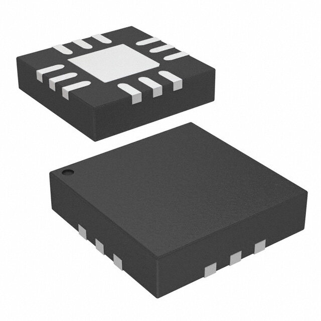
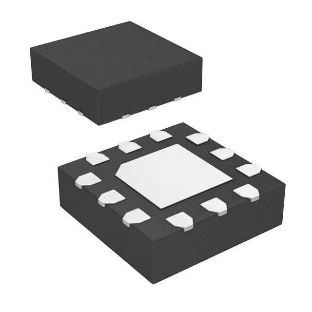
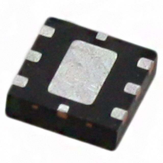
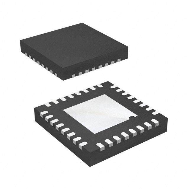
| 供应商器件封装 | 16-PQFN (4x4) |
| 关闭隔离—典型值 | 26.6 dB |
| 其它名称 | 1465-1351-6 |
| 包装 | Digi-Reel® |
| 商标 | MACOM |
| 封装 | Reel |
| 封装/外壳 | 16-VQFN 裸露焊盘 |
| 封装/箱体 | QFN-16 |
| 工作温度 | -40°C ~ 85°C |
| 工厂包装数量 | 1000 |
| 开关数量 | Single |
| 开关配置 | SPDT |
| 拓扑 | 反射 |
| 插损@频率 | 0.38dB @ 3.5GHz |
| 最大工作温度 | + 85 C |
| 最小工作温度 | - 40 C |
| 标准包装 | 1 |
| 特性 | - |
| 电压-电源 | 5V |
| 电源电流 | 50 mA |
| 电路 | SPDT |
| 系列 | MASW |
| 阻抗 | 50 欧姆 |
| 隔离@频率 | 36dB @ 3.5GHz (标准) |
| 频率 | 50 MHz to 6 GHz |
| 频率 -上 | 6GHz |
| 频率 -下 | 50MHz |


- 商务部:美国ITC正式对集成电路等产品启动337调查
- 曝三星4nm工艺存在良率问题 高通将骁龙8 Gen1或转产台积电
- 太阳诱电将投资9.5亿元在常州建新厂生产MLCC 预计2023年完工
- 英特尔发布欧洲新工厂建设计划 深化IDM 2.0 战略
- 台积电先进制程称霸业界 有大客户加持明年业绩稳了
- 达到5530亿美元!SIA预计今年全球半导体销售额将创下新高
- 英特尔拟将自动驾驶子公司Mobileye上市 估值或超500亿美元
- 三星加码芯片和SET,合并消费电子和移动部门,撤换高东真等 CEO
- 三星电子宣布重大人事变动 还合并消费电子和移动部门
- 海关总署:前11个月进口集成电路产品价值2.52万亿元 增长14.8%


PDF Datasheet 数据手册内容提取
MASW-000834 HMICTM PIN Diode SPDT 50 Watt Switch for 0.05 - 6.0 GHz Higher Power Applications Rev. V9 Features Functional Diagram (Top View) Exceptional Broadband Performance Low Loss: (Pin 16) T = 0.33 dB @ 2010 MHz, 5 V / 20 mA X N/C GND T GND T = 0.38 dB @ 3.5 GHz, 5 V / 20 mA X X High Isolation: (Pin 1) R = 44 dB @ 2010 MHz, 20 mA / 5 V X GND N/C R = 36 dB @ 3.5 GHz, 20 mA / 5 V X High T RF Input Power: X 50 W CW @ 2010 MHz ANT N/C High T RF Input Peak Power: X >1000 W GND N/C Suitable for Very High Power TD-SCDMA & WiMAX Applications Surface Mount 4 mm PQFN Package N/C DC2 RoHS* Compliant N/C GND R GND X Description and Applications The MASW-000834-13560T is a SPDT broadband, high linearity, common anode, PIN diode T/R switch, Pin Configuration2 for 0.05 - 6.0 GHz applications, including WiMAX & WiFi. The device is provided in industry standard 4 Pin Function Pin Function mm PQFN plastic packaging. This device incorporates a PIN diode die fabricated with 1 GND 9 DC2 MACOMs’ patented silicon-glass HMICTM process. 2 ANT 10 N/C This chip features two silicon pedestals embedded in a low loss, low dispersion glass. The diodes are 3 GND 11 N/C formed on the top of each pedestal. The topside is fully encapsulated with silicon nitride and has an 4 N/C 12 N/C additional polymer passivation layer that prevents 5 N/C 13 GND damage and contamination during handling and assembly. 6 GND 14 T X This compact SPDT switch offers wideband 7 R 15 GND X performance with excellent isolation to loss ratio for 8 GND 16 N/C both T and R states. The PIN diode provides X X 50 W typical CW power handling and 65 dBm IIP3 2. The exposed pad centered on the package bottom must be at 2010 MHz for maximum switch performance. connected to RF, DC and thermal ground. Ordering Information Part Number Package MASW-000834-13560T 1000 piece reel MASW-000834-001SMB Sample Board MADR-008851-0001TB1 Sample Board * Restrictions on Hazardous Substances, European Union Directive 2011/65/EU. 1. Sample board with recommended external driver & MASW-000834-13560T switch. 111 MACOM Technology Solutions Inc. (MACOM) and its affiliates reserve the right to make changes to the product(s) or information contained herein without notice. Visit www.macom.com for additional data sheets and product information. For further information and support please visit: https://www.macom.com/support DC-0008120
MASW-000834 HMICTM PIN Diode SPDT 50 Watt Switch for 0.05 - 6.0 GHz Higher Power Applications Rev. V9 Electrical Specifications3: T = +25°C, 20 mA / 5 V, P = 0 dBm, Z = 50 Ω A INC 0 Parameter Symbol Units Min. Typ. Max. F = 900 MHz R Insertion Loss, R X dB — 0.34 0.56 X IL T Insertion Loss, T X dB — 0.26 0.445 X IL R Isolation, ANT To R X dB 45.8 52.1 — X ISO T Isolation, ANT To T X dB 21.7 27.1 — X ISO F = 1800 MHz R Insertion Loss, R X dB — 0.40 0.72 X IL Tx Insertion Loss, T dB — 0.32 0.49 X IL Rx Isolation, ANT To R dB 43.7 48.9 — X ISO T Isolation, ANTTo T X dB 18.4 21.4 — X ISO F = 2010 MHz R Insertion Loss, R X dB — 0.42 0.75 X IL T Insertion Loss, T X dB — 0.33 0.5 X IL R Isolation, ANT To R X dB 43.2 44.6 — X ISO T Isolation, ANT To T X dB 17.7 19.9 — X ISO T Input Return Loss, T X dB — 32.1 — X RL R Input Return Loss, R X dB — 24.2 — X RL 3. See Bias Table 1. 222 MACOM Technology Solutions Inc. (MACOM) and its affiliates reserve the right to make changes to the product(s) or information contained herein without notice. Visit www.macom.com for additional data sheets and product information. For further information and support please visit: https://www.macom.com/support DC-0008120
MASW-000834 HMICTM PIN Diode SPDT 50 Watt Switch for 0.05 - 6.0 GHz Higher Power Applications Rev. V9 Electrical Specifications3: T = +25°C, 20 mA / 5 V, P = 0 dBm, Z = 50 Ω A INC 0 Parameter Symbol Units Min. Typ. Max. F = 2.3 - 2.7 GHz R Insertion Loss, R X dB — 0.46 0.84 X IL T Insertion Loss, T X dB — 0.35 0.525 X IL R Isolation, ANT To R X dB 40.2 41.2 — X ISO T Isolation, ANT To T X dB 16.2 18.6 — X ISO T Input Return Loss, T X dB — 30.5 — X RL R Input Return Loss, R X dB — 22.9 — X RL F = 3.3 - 3.8 GHz R Insertion Loss, R X dB — 0.56 1.0 X IL T Insertion Loss, T X dB — 0.38 0.575 X IL R Isolation, ANT To R X dB 33.7 35.9 — X ISO T Isolation, ANT To T X dB 13.6 16.1 — X ISO T Input Return Loss, T X dB — 27.4 — X RL R Input Return Loss, R X dB — 21.9 — X RL F = 4.9 - 5.9 GHz R Insertion Loss, R X dB — 0.78 — X IL T Insertion Loss, T X dB — 0.52 — X IL R Isolation, ANT To R X dB — 26.4 — X ISO T Isolation, ANT To T X dB — 11.8 — X ISO T — Input Return Loss, T X dB — 20.3 X RL R Input Return Loss, R X dB — 24.2 — X RL 333 MACOM Technology Solutions Inc. (MACOM) and its affiliates reserve the right to make changes to the product(s) or information contained herein without notice. Visit www.macom.com for additional data sheets and product information. For further information and support please visit: https://www.macom.com/support DC-0008120
MASW-000834 HMICTM PIN Diode SPDT 50 Watt Switch for 0.05 - 6.0 GHz Higher Power Applications Rev. V9 Electrical Specifications4: T = +25°C, 50 mA / 25 V, P = 0 dBm, Z = 50 Ω A INC 0 Parameter Symbol Units Min. Typ. Max. F = 900 MHz R Insertion Loss, R X dB — 0.27 — X IL T Insertion Loss, T X dB — 0.22 — X IL R Isolation, ANT To R X dB — 53.3 — X ISO T Isolation, ANT To T X dB — 27.4 — X ISO F = 1800 MHz R Insertion Loss, R X dB — 0.32 — X IL T Insertion Loss, T X dB — 0.27 — X IL R Isolation, ANT To R X dB — 50.2 — X ISO T Isolation, ANT To T X dB — 21.6 — X ISO F = 2010 MHz R Insertion Loss, R X dB — 0.34 — X IL T Insertion Loss, T X dB — 0.28 — X IL R Isolation, ANT To R X dB — 45.5 — X ISO T Isolation, ANT To T X dB — 20.1 — X ISO T Input Return Loss, T X dB — 33.1 — X RL R Input Return Loss, R X dB — 24.1 — X RL 4. See Bias Table 2. 444 MACOM Technology Solutions Inc. (MACOM) and its affiliates reserve the right to make changes to the product(s) or information contained herein without notice. Visit www.macom.com for additional data sheets and product information. For further information and support please visit: https://www.macom.com/support DC-0008120
MASW-000834 HMICTM PIN Diode SPDT 50 Watt Switch for 0.05 - 6.0 GHz Higher Power Applications Rev. V9 Electrical Specifications4: T = +25°C, 50 mA / 25 V, P = 0 dBm, Z = 50 Ω A INC 0 Parameter Symbol Units Min. Typ. Max. F = 2.3 - 2.7 GHz R Insertion Loss, R X dB — 0.38 — X IL T Insertion Loss, T X dB — 0.30 — X IL R Isolation, ANT To R X dB — 41.8 — X ISO T Isolation, ANT To T X dB — 18.7 — X ISO T Input Return Loss, T X dB — 31.3 — X RL R Input Return Loss, R X dB — 22.8 — X RL F = 3.3 - 3.8 GHz R Insertion Loss, R X dB — 0.47 — X IL T Insertion Loss, T X dB — 0.33 — X IL R Isolation, ANT To R X dB — 36.2 — X ISO T Isolation, ANT To T X dB — 16.2 — X ISO T Input Return Loss, T X dB — 28.0 — X RL R Input Return Loss, R X dB — 21.8 — X RL F = 4.9 - 5.9 GHz R Insertion Loss, R X dB — 0.72 — X IL T Insertion Loss, T X dB — 0.48 — X IL R Isolation, ANT To R X dB — 26.6 — X ISO T Isolation, ANT To T X dB — 11.8 — X ISO T Input Return Loss, T X dB — 20.5 — X RL R Input Return Loss, R X dB — 24.2 — X RL 555 MACOM Technology Solutions Inc. (MACOM) and its affiliates reserve the right to make changes to the product(s) or information contained herein without notice. Visit www.macom.com for additional data sheets and product information. For further information and support please visit: https://www.macom.com/support DC-0008120
MASW-000834 HMICTM PIN Diode SPDT 50 Watt Switch for 0.05 - 6.0 GHz Higher Power Applications Rev. V9 Electrical Specifications: T = +25°C, 50 mA / 25 V, Z = 50 Ω A 0 Parameter Symbol Test Conditions Units Min. Typ. Max. T 2010 MHz, T to Antenna >45.5 T Input P1dB X X dBm — — X P1dB 3.5 GHz, T to Antenna >45.0 X T 2010 MHz, P = +30 dBm 80 T 2nd Harmonic X IN dBc — — X 2Fo 3.5 GHz, P = +30 dBm 88 IN T 2010 MHz, P = +30 dBm 95 T 3rd Harmonic X IN dBc — — X 3Fo 3.5 GHz, P = +30 dBm 105 IN T P = +10 dBm, F1 = 2010 MHz, F2 = 2020 MHz >64 T Input IP3 X IN dBm — — X IIP3 P = +10 dBm, F1 = 3.50 GHz, F2 = 3.51 GHz >64 IN T T CW Input Power X F = 2010 MHz dBm / W — 47 / 50 — X P INC R F = 2010 MHz 41.5 / 14 R CW Input Power X dBm / W — — X P F = 3.5 GHz 40.5 / 11 INC F = 2010 MHz (10-90% RF Voltage) 200 T RF Switching Speed t F = 3.5 GHz (10-90% RF Voltage) ns — — X RF 200 1 MHz Rep Rate in Modulating Mode Absolute Maximum Ratings5,6 Static Sensitivity @ TA = +25°C (unless otherwise specified) These devices are rated Class 1B Human Body. Proper ESD control techniques should be used Parameter Absolute Maximum when handling these devices. Forward Current | 100 mA | RF & DC Reverse Voltage | -200 V | 50 W (47 dBm)7 T Incident CW Power X @ 2010 MHz T Peak Incident Power > 3 0 0 W, 5 µs, 1% duty X Junction Temperature +175°C Operating Temperature -40°C to +85°C Storage Temperature -55°C to +150°C 5. Exceeding these limits may cause permanent damage. 6. MACOM does not recommend sustained operation near these survivability limits. 7. Baseplate Temperature must be controlled to a constant +25°C. See derating curve. 666 MACOM Technology Solutions Inc. (MACOM) and its affiliates reserve the right to make changes to the product(s) or information contained herein without notice. Visit www.macom.com for additional data sheets and product information. For further information and support please visit: https://www.macom.com/support DC-0008120
MASW-000834 HMICTM PIN Diode SPDT 50 Watt Switch for 0.05 - 6.0 GHz Higher Power Applications Rev. V9 Typical Power Derating Curve T Maximum CW Input Power X (50 mA Forward Bias, 2010 MHz) 55 W) er ( 50 w o P ut 45 p n W I C 40 m u m xi 35 a M 30 25 45 65 85 Baseplate Temperature (°C) Note that this part must be held to a constant baseplate temperature to achieve the power handling results specified above. Adding a heatsink to the baseplate will improve performance to values greater than shown here. The increase in maximum input power from using a heatsink depends on the specific heatsink design. With a sample board mounted onto a heatsink of dimensions and fins shown below, this switch can handle up to 35 W CW of incident power. 777 MACOM Technology Solutions Inc. (MACOM) and its affiliates reserve the right to make changes to the product(s) or information contained herein without notice. Visit www.macom.com for additional data sheets and product information. For further information and support please visit: https://www.macom.com/support DC-0008120
MASW-000834 HMICTM PIN Diode SPDT 50 Watt Switch for 0.05 - 6.0 GHz Higher Power Applications Rev. V9 T Performance Curves @ +25°C, Z = 50 Ω X 0 T Insertion Loss, 20 mA & 50 mA T Isolation, 5 V & 25 V X X 0.0 0 -0.2 -10 B) s (d-0.4 dB)-20 ertion Los-0.6 solation (-30 s I n I-0.8 50 mA -40 25 V 20 mA 5 V -1.0 -50 0 1 2 3 4 5 6 0 1 2 3 4 5 6 Frequency (GHz) Frequency (GHz) R Performance Curves @ +25°C, Z = 50 Ω X 0 R Insertion Loss, 20 mA & 50 mA R Isolation, 5 V & 25 V X X 0.0 0 -0.2 50 mA -10 25 V 20 mA 5 V B) s (d-0.4 dB)-20 ertion Los-0.6 solation (-30 s I n I -0.8 -40 -1.0 -50 0 1 2 3 4 5 6 0 1 2 3 4 5 6 Frequency (GHz) Frequency (GHz) 888 MACOM Technology Solutions Inc. (MACOM) and its affiliates reserve the right to make changes to the product(s) or information contained herein without notice. Visit www.macom.com for additional data sheets and product information. For further information and support please visit: https://www.macom.com/support DC-0008120
MASW-000834 HMICTM PIN Diode SPDT 50 Watt Switch for 0.05 - 6.0 GHz Higher Power Applications Rev. V9 Bias Diagrams & Tables8 T -ANT Insertion Loss, R -ANT Isolation R -ANT Insertion Loss, T -ANT Isolation X X X X (Pin 16) (Pin 16) N/C GND T GND N/C GND T GND X X (Pin 1) (Pin 1) + GND 2200mmAA // 5500mmAA N/C GND 5V / 25V 20mA / 50mA N/C - ANT N/C ANT N/C -- - GND 5V 5/ V2 5/ V25V N/C GND 5V / 25V N/C 20mA / 50mA ++ 2200mmAA // 5500mmAA + - 205mV A/ 2/ 55V0mA+ N/C DC2 N/C DC2 N/C GND R GND N/C GND R GND X X Bias Table 1 T R DC2 ANT X X Parameter Pin 14 Pin 7 Pin 9 Pin 2 T -ANT Insertion Loss X -20 mA +5 V, +20 mA -20 mA 0 V, +20 mA R -ANT Isolation X R -ANT Insertion Loss X +5 V, 0 mA -20 mA +5 V, 0 mA 0 V, +20 mA T -ANT Isolation X Bias Table 2 T R DC2 ANT X X Parameter Pin 14 Pin 7 Pin 9 Pin 2 T -ANT Insertion Loss X -50 mA +25 V, +50 mA -50 mA 0 V, +50 mA R -ANT Isolation X R -ANT Insertion Loss X +25 V, 0 mA -50 mA +25 V, 0 mA 0 V, +50 mA T -ANT Isolation X 8. Diode Based Products require different minimum reverse bias voltages depending on the frequency and incident power levels. More details can be found on page 10 of this datasheet. 999 MACOM Technology Solutions Inc. (MACOM) and its affiliates reserve the right to make changes to the product(s) or information contained herein without notice. Visit www.macom.com for additional data sheets and product information. For further information and support please visit: https://www.macom.com/support DC-0008120
MASW-000834 HMICTM PIN Diode SPDT 50 Watt Switch for 0.05 - 6.0 GHz Higher Power Applications Rev. V9 Minimum Required Reverse Bias Voltage Minimum reverse bias voltage on a PIN diode based product varies with frequency of operation and incident power levels. As a rule of thumb, a designer can always use the magnitude of the peak RF voltage or empirically locate lower bias values than the peak RF voltage magnitude. However, it has been shown that lower DC voltages can be used depending on the RF environment in which a diode is placed. In the plot below, the minimum required reverse voltage vs. frequency is shown for an incident RF power of 50 Watts. This trend line will shift lower if the incident RF power is decreased. The biasing values have not been verified through measurement at MACOM. As a result, please use the data below as a guide only for biasing requirements as this data is based solely on generic PIN diode equations.9 Please be cautious in that lower reverse bias levels can degrade isolation and distortion in a PIN diode based product. 9. R. Caverly and G. Hiller, “Establishing the Minimum Reverse Bias for a P-I-N Diode in a High Power Switch,” IEEE Transactions on Micro- wave Theory and Techniques, Vol.38, No.12, December 1990. Reverse Bias Required vs. Frequency (50 W Power Handling) 80 70 V) e ( 60 g olta 50 V s 40 a Bi e 30 s er v 20 e R 10 0 0 500 1000 1500 2000 Frequency (MHz) 111000 MACOM Technology Solutions Inc. (MACOM) and its affiliates reserve the right to make changes to the product(s) or information contained herein without notice. Visit www.macom.com for additional data sheets and product information. For further information and support please visit: https://www.macom.com/support DC-0008120
MASW-000834 HMICTM PIN Diode SPDT 50 Watt Switch for 0.05 - 6.0 GHz Higher Power Applications Rev. V9 MASW-000834 and Recommended Driver with +5 V & +28 V DC Power10,11,12,13,14,15,16,17 MADR-008851 is the recommended driver for the MASW-000834 Switch. Part Value C1-C3 27 pF, 100 V ANT C4 1000 pF C5 0.022 µF C3 C6,C7 12 pF L1 R111 C813 20 pF +5 V L1, L2, L3,L4 27 nH C4 C5 R1 see note 11 R2 see note 12 T Voltage X R Voltage X TX RX C1 C2 SPDT L2 L3 C813 +28 V +5 V L4 C6 C7 TX SH Current R X Logic C1 SH2 Input MADR-008851-000100 R210 Switch Driver SH1 Ground 10. Forward Bias Diode Voltage: DV is ~0.9 V @ 22 mA; DV is ~1.0 V @ 35 mA F F 11. R1 is calculated by (V - 1.5 V)/I , where I is the desired bias current for the series diodes: CC SERIES SERIES For 21 mA load current, R1 = 165 Ω @ V = 5.0 V and 82 Ω @ V = 3.3 V. CC CC For 32 mA load current, R1 = 110 Ω @ V = 5.0 V and 56 Ω @ V = 3.3 V. CC CC 12. R2 is calculated by (V - 1.0 V)/I , where I is the desired forward bias current for the shunt diode. The power dissipation is DD SHUNT SHUNT calculated by I x 27 V. For 20 mA of I , R2 should use a 2511, 1W, 1.3k Ω resistor. SHUNT SHUNT 13. C8 is already built-in for MASW-000834-13560T switch. 14. The voltage at the common anode will be approximately 1.5 V. 15. The current in through the back-biased diodes will be the leakage current for the diodes. 16. C1-C5, L1-L4, R1, R2, and the switch are discrete components that should be installed on the users board. It is recommended that Coil- craft 0603CS-27NXJLW or equivalent be used for L1-L4 at 2 GHz (values may vary based on the frequency). 17. There are 33 pF bypass capacitors included in the driver for the R , T , and SH1 ports. There are cases (especially at higher frequen- X X cies), where the optional 12 pF bypass capacitors (C6 and C7) that are shown on the schematic are needed. 111111 MACOM Technology Solutions Inc. (MACOM) and its affiliates reserve the right to make changes to the product(s) or information contained herein without notice. Visit www.macom.com for additional data sheets and product information. For further information and support please visit: https://www.macom.com/support DC-0008120
MASW-000834 HMICTM PIN Diode SPDT 50 Watt Switch for 0.05 - 6.0 GHz Higher Power Applications Rev. V9 Outline: 4 mm PQFN 16-Lead Saw Singulated † Reference Application Note S2083 for lead-free solder reflow recommendations. Meets JEDEC moisture sensitivity level 1 requirements. 111222 MACOM Technology Solutions Inc. (MACOM) and its affiliates reserve the right to make changes to the product(s) or information contained herein without notice. Visit www.macom.com for additional data sheets and product information. For further information and support please visit: https://www.macom.com/support DC-0008120
MASW-000834 HMICTM PIN Diode SPDT 50 Watt Switch for 0.05 - 6.0 GHz Higher Power Applications Rev. V9 MACOM Technology Solutions Inc. All rights reserved. Information in this document is provided in connection with MACOM Technology Solutions Inc ("MACOM") products. These materials are provided by MACOM as a service to its customers and may be used for informational purposes only. Except as provided in MACOM's Terms and Conditions of Sale for such products or in any separate agreement related to this document, MACOM assumes no liability whatsoever. MACOM assumes no responsibility for errors or omissions in these materials. MACOM may make changes to specifications and product descriptions at any time, without notice. MACOM makes no commitment to update the information and shall have no responsibility whatsoever for conflicts or incompatibilities arising from future changes to its specifications and product descriptions. No license, express or implied, by estoppels or otherwise, to any intellectual property rights is granted by this document. THESE MATERIALS ARE PROVIDED "AS IS" WITHOUT WARRANTY OF ANY KIND, EITHER EXPRESS OR IMPLIED, RELATING TO SALE AND/OR USE OF MACOM PRODUCTS INCLUDING LIABILITY OR WARRANTIES RELATING TO FITNESS FOR A PARTICULAR PURPOSE, CONSEQUENTIAL OR INCIDENTAL DAMAGES, MERCHANTABILITY, OR INFRINGEMENT OF ANY PATENT, COPYRIGHT OR OTHER INTELLECTUAL PROPERTY RIGHT. MACOM FURTHER DOES NOT WARRANT THE ACCURACY OR COMPLETENESS OF THE INFORMATION, TEXT, GRAPHICS OR OTHER ITEMS CONTAINED WITHIN THESE MATERIALS. MACOM SHALL NOT BE LIABLE FOR ANY SPECIAL, INDIRECT, INCIDENTAL, OR CONSEQUENTIAL DAMAGES, INCLUDING WITHOUT LIMITATION, LOST REVENUES OR LOST PROFITS, WHICH MAY RESULT FROM THE USE OF THESE MATERIALS. MACOM products are not intended for use in medical, lifesaving or life sustaining applications. MACOM customers using or selling MACOM products for use in such applications do so at their own risk and agree to fully indemnify MACOM for any damages resulting from such improper use or sale. 111333 MACOM Technology Solutions Inc. (MACOM) and its affiliates reserve the right to make changes to the product(s) or information contained herein without notice. Visit www.macom.com for additional data sheets and product information. For further information and support please visit: https://www.macom.com/support DC-0008120