ICGOO在线商城 > 射频/IF 和 RFID > RF 开关 > HMC849LP4CE
 Datasheet下载
- 型号: HMC849LP4CE
- 制造商: Hittite
- 库位|库存: xxxx|xxxx
- 要求:
| 数量阶梯 | 香港交货 | 国内含税 |
| +xxxx | $xxxx | ¥xxxx |
查看当月历史价格
查看今年历史价格
HMC849LP4CE产品简介:
ICGOO电子元器件商城为您提供HMC849LP4CE由Hittite设计生产,在icgoo商城现货销售,并且可以通过原厂、代理商等渠道进行代购。 HMC849LP4CE价格参考。HittiteHMC849LP4CE封装/规格:RF 开关, RF Switch IC General Purpose SPDT 6GHz 50Ohm 16-QFN (4x4)。您可以下载HMC849LP4CE参考资料、Datasheet数据手册功能说明书,资料中有HMC849LP4CE 详细功能的应用电路图电压和使用方法及教程。
HMC849LP4CE是Analog Devices Inc.(ADI)推出的一款高性能GaAs MMIC射频开关,属于RF开关类别。该器件采用SMT封装(4x4mm QFN),工作频率范围覆盖DC至6 GHz,适用于宽带通信系统。

主要应用场景包括:
1. 无线通信系统:广泛用于蜂窝基站、微波点对点通信和无线回传系统中,实现发射与接收通道的快速切换,支持多频段操作。
2. 国防与航空航天:在雷达系统、电子战设备和军用通信中,用于高频信号路径控制,具备高隔离度和低插入损耗,确保信号完整性。
3. 测试与测量仪器:应用于矢量网络分析仪、信号发生器等设备中,作为内部射频路径切换元件,提升测试精度与系统灵活性。
4. 宽带基础设施:支持5G基础设施中的射频前端模块,适用于需要高可靠性与稳定性能的场景。

HMC849LP4CE为单刀双掷(SPDT)开关,具有+37dBm的高输入IP3,保证在强信号环境下仍能保持良好线性性能;同时提供TTL/CMOS兼容控制接口,便于与数字系统集成。其紧凑型封装适合高密度PCB布局,适用于对空间敏感的射频设计。

综上,HMC849LP4CE是一款适用于通信、军工与测试领域的高性能宽带RF开关,具备优良的电气性能与环境适应性。
| 参数 | 数值 |
| 产品目录 | |
| 描述 | IC SW GASS PHEMT SPDT 16QFN |
| 产品分类 | |
| IIP3 | 52dBm (标准) |
| 品牌 | Hittite Microwave Corporation |
| 数据手册 | |
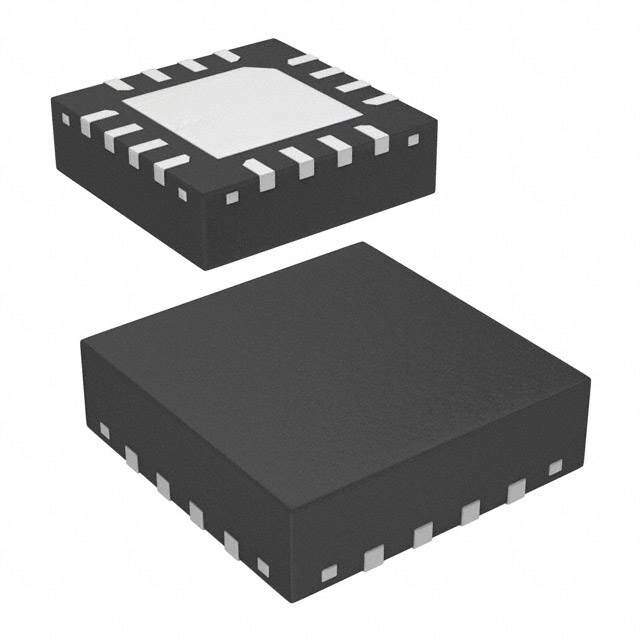
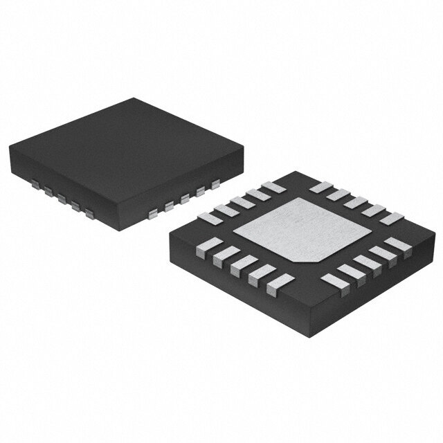
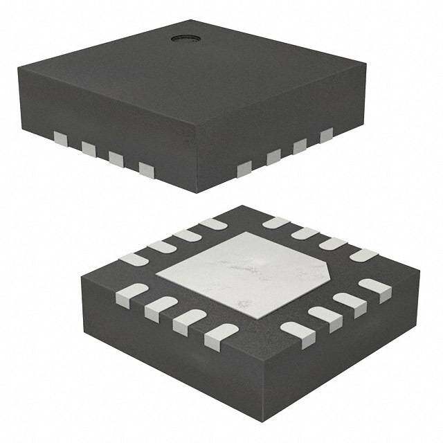
| 产品图片 |
|
| P1dB | 35dBm (标准) IP1dB |
| 产品型号 | HMC849LP4CE |
| RF类型 | 通用 |
| rohs | 无铅 / 符合限制有害物质指令(RoHS)规范要求 |
| 产品系列 | - |
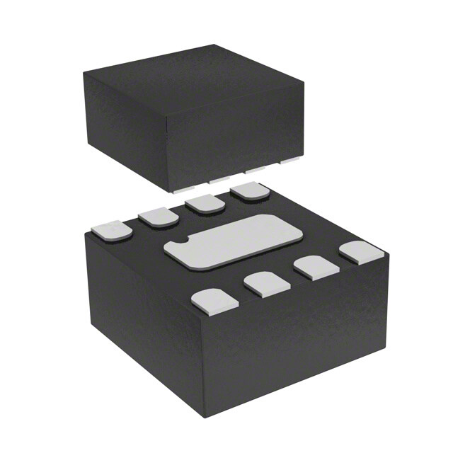
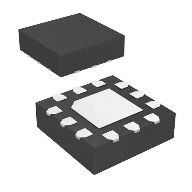
| 供应商器件封装 | 16-QFN(4x4) |
| 其它名称 | 1127-1072-1 |
| 包装 | 剪切带 (CT) |
| 封装/外壳 | 16-VQFN 裸露焊盘 |
| 工作温度 | -40°C ~ 85°C |
| 拓扑 | 吸收性 |
| 插损@频率 | 1.7dB @ 6GHz |
| 标准包装 | 1 |
| 特性 | - |
| 电压-电源 | - |
| 电路 | SPDT |
| 阻抗 | 50 欧姆 |
| 隔离@频率 | 52dB @ 6GHz (标准) |
| 频率 -上 | 6GHz |
| 频率 -下 | DC |


- 商务部:美国ITC正式对集成电路等产品启动337调查
- 曝三星4nm工艺存在良率问题 高通将骁龙8 Gen1或转产台积电
- 太阳诱电将投资9.5亿元在常州建新厂生产MLCC 预计2023年完工
- 英特尔发布欧洲新工厂建设计划 深化IDM 2.0 战略
- 台积电先进制程称霸业界 有大客户加持明年业绩稳了
- 达到5530亿美元!SIA预计今年全球半导体销售额将创下新高
- 英特尔拟将自动驾驶子公司Mobileye上市 估值或超500亿美元
- 三星加码芯片和SET,合并消费电子和移动部门,撤换高东真等 CEO
- 三星电子宣布重大人事变动 还合并消费电子和移动部门
- 海关总署:前11个月进口集成电路产品价值2.52万亿元 增长14.8%


PDF Datasheet 数据手册内容提取
HMC849LP4CE v04.0613 HIGH ISOLATION SPDT NON-REFLECTIVE SWITCH, DC - 6 GHz Typical Applications Features The HMC849LP4CE is ideal for: High Isolation: up to 60 dB T • Cellular/4G Infrastructure Single Positive Control: 0/+3V to +5V M • WiMAX, WiBro & Fixed Wireless High Input IP3: +52 dBm S • Automotive Telematics Non-Reflective Design - T • Mobile Radio “All Off” State D • Test Equipment 16 Lead 4x4 mm QFN Package: 16 mm² P S - Functional Diagram General Description S E The HMC849LP4CE is a high isolation non-reflec- H tive DC to 6 GHz GaAs pHEMT SPDT switch in a low C cost leadless surface mount package. The switch is T ideal for cellular/WiMAX/4G Infrastructure applicati- I W ons yielding up to 60 dB isolation, low 0.8 dB inser- S tion loss and +52 dBm input IP3. Power handling is excellent up through the 5 - 6 GHz WiMAX band with the switch offering a P1dB compression point of +31 dBm. On-chip circuitry allows a single positive voltage control of 0/+3V or 0/+5V at very low DC currents. An enable input (EN) set to logic high will put the switch in an “all off” state. Electrical Specifications, T = +25 °C, Vctl = 0/Vdd, Vdd = +3V to +5V, 50 Ohm System A Parameter Frequency Min. Typ. Max. Units DC - 2.0 GHz 0.8 1.3 dB Insertion Loss 2.0 - 4.0 GHz 1.0 1.5 dB 4.0 - 6.0 GHz 1.7 2.5 DC - 2.0 GHz 53 60 dB Isolation (RFC to RF1/RF2) 2.0 - 4.0 GHz 48 55 dB 4.0 - 6.0 GHz 40 52 DC - 4.0 GHz 17 dB Return Loss (On State) 4.0 - 6.0 GHz 13 dB Return Loss (Off State) DC - 6.0 GHz 15 dB +3V 29 30 dBm Input Power for 1 dB Compression 0.35 - 4.0 GHz +5V 34 35 dBm Input Third Order Intercept DC - 6.0 GHz 52 dBm (Two-Tone Input Power = +7 dBm Each Tone) Switching Speed tRISE, tFALL (10/90% RF) DC - 4.0 GHz 80 ns tON, tOFF (50% CTL to 10/90% RF) 150 600 ns For price, delivery and to place orders: Hittite Microwave Corporation, 2 Elizabeth Drive, Chelmsford, MA 01824 1 Phone: 978-250-3343 Fax: 978-250-3373 Order On-line at www.hittite.com Application Support: Phone: 978-250-3343 or apps@hittite.com
HMC849LP4CE v04.0613 HIGH ISOLATION SPDT NON-REFLECTIVE SWITCH, DC - 6 GHz Insertion Loss Return Loss [1] 0 0 -0.5 -5 T SS (dB)-1-.51 S (dB) --1150 SM O S NSERTION L-2--.532 RETURN LO ---322050 DT - I -3.5 -35 P -4 -40 S 0 1 2 3 4 5 6 7 0 1 2 3 4 5 6 7 FREQUENCY (GHz) FREQUENCY (GHz) - +25C S RFC +-4805CC RRFF11,, RRFF22 OOFNF E H Isolation Between C Ports RFC and RF1 / RF2 Isolation Between Ports RF1 and RF2 T I 0 0 W -10 S -20 -20 N (dB)-40 N (dB)-30 O O-40 TI TI OLA-60 OLA-50 S S I I -60 -80 -70 -100 -80 0 1 2 3 4 5 6 7 0 1 2 3 4 5 6 7 FREQUENCY (GHz) FREQUENCY (GHz) RF1 RFC-RF1 ON RF2 RFC-RF2 ON ALL OFF 0.1 and 1 dB Input Compression 0.1 and 1 dB Input Compression Point, Vdd = 5V, Linear Point, Vdd = 3V, Linear 40 35 dBm) 35 dBm) 30 N ( N ( O O SI 30 SI S S RE RE 25 P P M 25 M O O C C UT UT 20 P 20 P N N I I 15 15 0 1 2 3 4 5 6 0 1 2 3 4 5 6 FREQUENCY (GHz) FREQUENCY (GHz) 0.1 dB Compression Point 0.1 dB Compression Point 1dB Compression Point 1 dB Compression Point [1] RFC is reflective in “all off” state. For price, delivery and to place orders: Hittite Microwave Corporation, 2 Elizabeth Drive, Chelmsford, MA 01824 Phone: 978-250-3343 Fax: 978-250-3373 Order On-line at www.hittite.com 2 Application Support: Phone: 978-250-3343 or apps@hittite.com
HMC849LP4CE v04.0613 HIGH ISOLATION SPDT NON-REFLECTIVE SWITCH, DC - 6 GHz 0.1 and 1 dB Input Compression 0.1 and 1 dB Input Compression Point, Vdd = 5V Point, Vdd = 3V 40 35 MT N (dBm) 35 N (dBm) 30 O O S SI 30 SI S S RE RE 25 - P P T COM 25 COM D UT UT 20 P 20 P N N P I I S 15 15 0.01 0.1 1 0.01 0.1 1 - FREQUENCY (GHz) in log scale FREQUENCY (GHz) in log scale S 0.1 dB Compression Point 0.1 dB Compression Point E 1 dB Compression Point 1 dB Compression Point H C Input Third Order Intercept Input Third Order Intercept T Point, Vdd = 5V, Linear Point, Vdd = 3V, Linear I W 60 60 S 55 55 m) m) B B 3 (d 50 3 (d 50 P P I I 45 45 40 40 0 1 2 3 4 5 6 0 1 2 3 4 5 6 FREQUENCY (GHz) FREQUENCY (GHz) +25C +25C +85C +85C -40C -40C Input Third Order Intercept Input Third Order Intercept Point, Vdd = 5V Point, Vdd = 3V 60 60 55 55 m) m) B B 3 (d 50 3 (d 50 P P I I 45 45 40 40 0.01 0.1 1 0.01 0.1 1 FREQUENCY (GHz) in log scale FREQUENCY (GHz) in log scale +25C +25C +85C +85C -40C -40C For price, delivery and to place orders: Hittite Microwave Corporation, 2 Elizabeth Drive, Chelmsford, MA 01824 3 Phone: 978-250-3343 Fax: 978-250-3373 Order On-line at www.hittite.com Application Support: Phone: 978-250-3343 or apps@hittite.com
HMC849LP4CE v04.0613 HIGH ISOLATION SPDT NON-REFLECTIVE SWITCH, DC - 6 GHz Absolute Maximum Ratings Bias Voltage & Current Bias Voltage (Vdd) 7V Vdd Idd (Typ.) (V) (mA) Control Voltage (Vctl, EN) -1V to Vdd +1V T RF Input Power * 3 0.80 M Through Path 3V/5V 30.60 / 33 dBm 5 0.85 S Termination Path 3V/5V 26.4 dBm - Channel Temperature 150 °C T Digital Control Voltages Continuous Pdiss (T = 85 °C) D (derate 17.6 mW/°C for through path, and 6.8 mW/°C for termination path above 85 °C) State Bias Condition P Through Path 1.144 W Low 0 to +0.8 Vdc @ <1 µA Typical S Termination Path 0.441 W High +2.0 to +5.0 Vdc @ 30 µA Typical - Thermal Resistance S (channel to package bottom) Through Path 56.8 °C/W E Termination Path 147.3 °C/W Truth Table H Storage Temperature -65 to +150 °C C Control Input Signal Path State Operating Temperature -40 to +85 °C T Vctl EN RFC - RF1 RFC - RF2 I ESD Sensitivity (HBM) Class 1A W Low Low OFF ON * The RF input power is quite lower than the breakdown High Low ON OFF S power levels. Hence, the only concern with this product Low High OFF OFF is the thermal limit. High High OFF OFF ELECTROSTATIC SENSITIVE DEVICE OBSERVE HANDLING PRECAUTIONS For price, delivery and to place orders: Hittite Microwave Corporation, 2 Elizabeth Drive, Chelmsford, MA 01824 Phone: 978-250-3343 Fax: 978-250-3373 Order On-line at www.hittite.com 4 Application Support: Phone: 978-250-3343 or apps@hittite.com
HMC849LP4CE v04.0613 HIGH ISOLATION SPDT NON-REFLECTIVE SWITCH, DC - 6 GHz Outline Drawing T M S - T D P S - S E H C T I W S NOTES: 1. LEADFRAME MATERIAL: COPPER ALLOY 2. DIMENSIONS ARE IN INCHES [MILLIMETERS] 3. LEAD SPACING TOLERANCE IS NON-CUMULATIVE. 4. PAD BURR LENGTH SHALL BE 0.15mm MAXIMUM. PAD BURR HEIGHT SHALL BE 0.05mm MAXIMUM. 5. PACKAGE WARP SHALL NOT EXCEED 0.05mm. 6. ALL GROUND LEADS AND GROUND PADDLE MUST BE SOLDERED TO PCB RF GROUND. 7. REFER TO HITTITE APPLICATION NOTE FOR SUGGESTED LAND PATTERN. Package Information Part Number Package Body Material Lead Finish MSL Rating Package Marking [1] HMC849LP4CE RoHS-compliant Low Stress Injection Molded Plastic 100% matte Sn MSL1 [2] H849 XXXX [1] 4-Digit lot number XXXX [2] Max peak reflow temperature of 260 °C For price, delivery and to place orders: Hittite Microwave Corporation, 2 Elizabeth Drive, Chelmsford, MA 01824 5 Phone: 978-250-3343 Fax: 978-250-3373 Order On-line at www.hittite.com Application Support: Phone: 978-250-3343 or apps@hittite.com
HMC849LP4CE v04.0613 HIGH ISOLATION SPDT NON-REFLECTIVE SWITCH, DC - 6 GHz Pin Descriptions Pin Number Function Description Interface Schematic 1 Vdd Supply Voltage. T M S 2 Vctl Control input. See truth and control voltage tables. - T D P 3, 9, 12 RFC, RF1, RF2 These pins are DC coupled and matched to 50 Ohms. S Blocking capacitors are required. - The pins are not connected internally; however, all 4, 6, 7, 8, S N/C data shown herein was measured with these pins 13, 14, 15, 16 E connected to RF/DC ground externally. H C T 5 EN Enable. See truth and control voltage tables. I W S Package bottom must also be 10, 11 GND connected to PCB RF ground. Application Circuit For price, delivery and to place orders: Hittite Microwave Corporation, 2 Elizabeth Drive, Chelmsford, MA 01824 Phone: 978-250-3343 Fax: 978-250-3373 Order On-line at www.hittite.com 6 Application Support: Phone: 978-250-3343 or apps@hittite.com
HMC849LP4CE v04.0613 HIGH ISOLATION SPDT NON-REFLECTIVE SWITCH, DC - 6 GHz Evaluation PCB T M S - T D P S - S E H C T I W S List of Materials for Evaluation PCB 106975 [1] The circuit board used in the final application Item Description should be generated with proper RF circuit design J1 - J3 PC Mount SMA RF Connector techniques. Signal lines at the RF port should have J4 - J8 DC Pin 50 Ohm impedance and the package ground leads C1 - C4 100 pF Capacitor, 0402 Pkg. and backside ground slug should be connected U1 HMC849LP4CE SPDT Switch directly to the ground plane similar to that shown PCB [2] 106965 Evaluation PCB above. The evaluation circuit board shown above is [1] Reference this number when ordering complete evaluation PCB available from Hittite Microwave Corporation upon [2] Circuit Board Material: Rogers 4350 or Arlon 25FR request. For price, delivery and to place orders: Hittite Microwave Corporation, 2 Elizabeth Drive, Chelmsford, MA 01824 7 Phone: 978-250-3343 Fax: 978-250-3373 Order On-line at www.hittite.com Application Support: Phone: 978-250-3343 or apps@hittite.com
HMC849LP4CE v04.0613 HIGH ISOLATION SPDT NON-REFLECTIVE SWITCH, DC - 6 GHz Notes: T M S - T D P S - S E H C T I W S For price, delivery and to place orders: Hittite Microwave Corporation, 2 Elizabeth Drive, Chelmsford, MA 01824 Phone: 978-250-3343 Fax: 978-250-3373 Order On-line at www.hittite.com 8 Application Support: Phone: 978-250-3343 or apps@hittite.com