ICGOO在线商城 > 射频/IF 和 RFID > RF 开关 > HMC174MS8E
 Datasheet下载
- 型号: HMC174MS8E
- 制造商: Hittite
- 库位|库存: xxxx|xxxx
- 要求:
| 数量阶梯 | 香港交货 | 国内含税 |
| +xxxx | $xxxx | ¥xxxx |
查看当月历史价格
查看今年历史价格
HMC174MS8E产品简介:
ICGOO电子元器件商城为您提供HMC174MS8E由Hittite设计生产,在icgoo商城现货销售,并且可以通过原厂、代理商等渠道进行代购。 HMC174MS8E价格参考。HittiteHMC174MS8E封装/规格:RF 开关, 射频开关 IC WiMax SPDT 3GHz 50 欧姆 8-MSOP。您可以下载HMC174MS8E参考资料、Datasheet数据手册功能说明书,资料中有HMC174MS8E 详细功能的应用电路图电压和使用方法及教程。
HMC174MS8E 是 Analog Devices Inc.(ADI)生产的一款 RF 开关,属于高性能单刀双掷 (SPDT) 开关。其典型应用场景包括无线通信系统、测试测量设备、雷达系统以及卫星通信等领域。以下是该型号的具体应用场景及特点:

1. 无线基础设施:
   HMC174MS8E 适用于基站和中继器中的射频信号切换。它支持高达 20 GHz 的频率范围,适合用于 LTE、5G 和其他宽带无线通信系统的信号路径选择。

2. 测试与测量:
   在测试设备中,这款开关可以用来快速切换不同的信号源或负载,同时保持低插入损耗和高隔离度,确保测试结果的准确性。

3. 雷达系统:
   雷达应用需要快速切换发射和接收模式,HMC174MS8E 提供了快速的开关速度(小于 50 ns),能够满足现代雷达系统的严格要求。

4. 卫星通信:
   由于其宽广的工作频率范围和良好的线性性能,HMC174MS8E 可以用作卫星通信链路中的信号路由组件,帮助实现多频段操作。

5. 点对点微波通信:
   在固定无线接入网络中,该器件可用于选择不同的天线方向或频段,从而优化链路效率。

6. 航空航天与国防:
   这款开关以其高可靠性、耐高温特性和优异的电气性能,成为航空航天和国防领域的重要选择,例如在无人机、导航系统和电子战设备中。

总结来说,HMC174MS8E 凭借其低插入损耗(典型值为 0.9 dB)、高隔离度(大于 35 dB)以及出色的线性性能(IP3 超过 +50 dBm),非常适合需要高性能射频信号切换的各种复杂环境。
| 参数 | 数值 |
| 产品目录 | |
| 描述 | IC MMIC SWITCH GAAS 3GHZ 8-MSOP |
| 产品分类 | |
| IIP3 | 56dBm |
| 品牌 | Hittite Microwave Corporation |
| 数据手册 | |
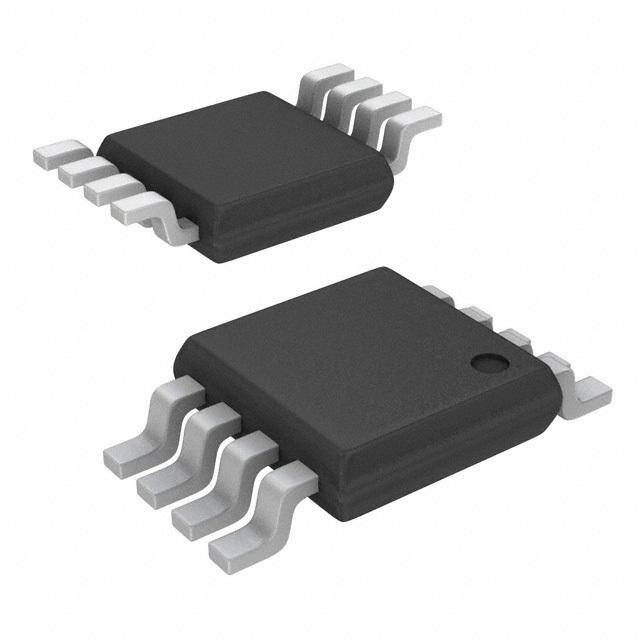
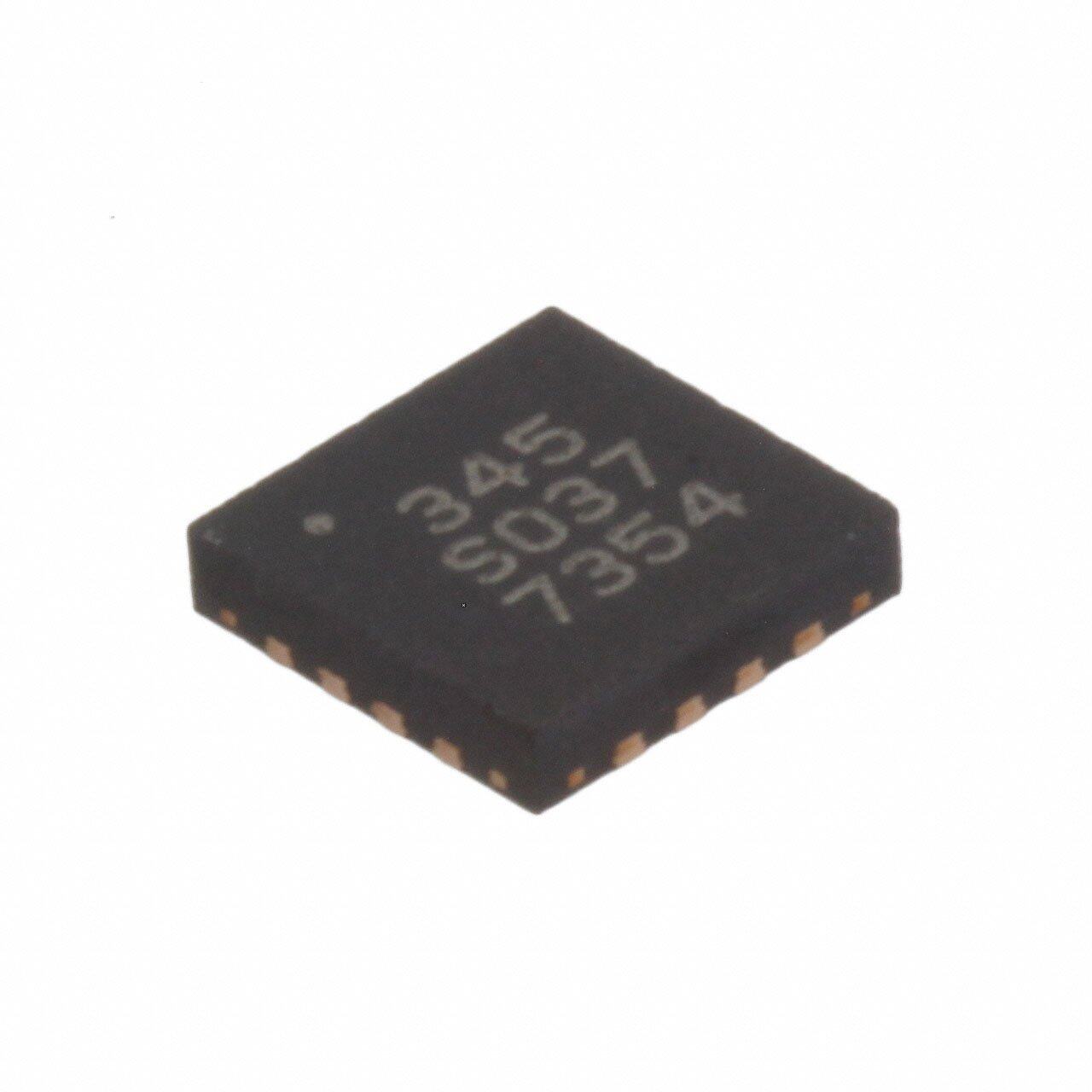
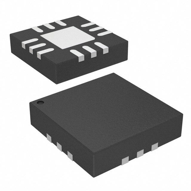
| 产品图片 |
|
| P1dB | 36dBm (标准) IP1dB |
| 产品型号 | HMC174MS8E |
| RF类型 | WiMax |
| rohs | 无铅 / 符合限制有害物质指令(RoHS)规范要求 |
| 产品系列 | - |
| 供应商器件封装 | 8-MSOP |
| 其它名称 | 1127-1294 |
| 包装 | 剪带 |
| 封装/外壳 | 8-TSSOP,8-MSOP(0.118",3.00mm 宽) |
| 工作温度 | -40°C ~ 85°C |
| 拓扑 | 反射 |
| 插损@频率 | 1.3dB @ 3GHz |
| 标准包装 | 100 |
| 特性 | - |
| 电压-电源 | 3 V ~ 8 V |
| 电路 | SPDT |
| 阻抗 | 50 欧姆 |
| 隔离@频率 | 20dB @ 3GHz (标准) |
| 频率 -上 | 3GHz |
| 频率 -下 | DC |


- 商务部:美国ITC正式对集成电路等产品启动337调查
- 曝三星4nm工艺存在良率问题 高通将骁龙8 Gen1或转产台积电
- 太阳诱电将投资9.5亿元在常州建新厂生产MLCC 预计2023年完工
- 英特尔发布欧洲新工厂建设计划 深化IDM 2.0 战略
- 台积电先进制程称霸业界 有大客户加持明年业绩稳了
- 达到5530亿美元!SIA预计今年全球半导体销售额将创下新高
- 英特尔拟将自动驾驶子公司Mobileye上市 估值或超500亿美元
- 三星加码芯片和SET,合并消费电子和移动部门,撤换高东真等 CEO
- 三星电子宣布重大人事变动 还合并消费电子和移动部门
- 海关总署:前11个月进口集成电路产品价值2.52万亿元 增长14.8%


PDF Datasheet 数据手册内容提取
HMC174MS8 174MS8E / v04.0109 GaAs MMIC T/R SWITCH DC - 3 GHz Typical Applications Features The HMC174MS8(E) is ideal for: Low Insertion Loss: 0.5 dB • Infrastructure & Repeaters High Input IP3: +60 dBm • Cellular/3G & WiMAX Positive Control: 0/+3V to 0 /+8V • Portable Wireless High RF power Capability • LNA Protection MSOP - 8 SMT package, 14.8 mm2 • Automotive Telematics • Test Equipment Functional Diagram General Description The HMC174MS8 & HMC174MS8E are low-cost SPDT switches in 8-lead MSOP packages for use in 11 transmit-receive applications which require very low distortion at high signal power levels. The device can control signals from DC to 3 GHz and is especially T suited for cellular/3G and WiMAX applications with M only 0.5 dB loss. The design provides exceptional S intermodulation performance; providing a +60 dBm third order intercept at 8 Volt bias. RF1 and RF2 are - refl ective shorts when “OFF”. On chip circuitry allows R single positive supply operation at very low DC current / T with control inputs compatible with CMOS and most T TTL logic families. D P S Electrical Specifi cations, T = +25° C, Vdd = +5 Vdc, 50 Ohm System A - Parameter Frequency Min. Typ. Max. Units S DC - 1.0 GHz 0.4 0.7 dB E DC - 2.0 GHz 0.5 0.8 dB Insertion Loss H DC - 2.5 GHz 0.8 1.1 dB DC - 3.0 GHz 1.3 1.8 dB C DC - 1.0 GHz 21 26 dB T DC - 2.0 GHz 21 26 dB I Isolation DC - 2.5 GHz 18 23 dB W DC - 3.0 GHz 15 20 dB S DC - 1.0 GHz 25 dB DC - 2.0 GHz 20 dB Return Loss DC - 2.5 GHz 15 dB DC - 3.0 GHz 12 dB 0.5 - 1.0 GHz 32 36 dBm Input Power for 1 dB Compression 0/8V Control 0.5 - 3.0 GHz 32 36 dBm 0.5 - 1.0 GHz 55 60 dBm Input Third Order Intercept 0/8V Control 0.5 - 3.0 GHz 49 56 dBm Switching Characteristics DC - 3.0 GHz tRISE, tFALL (10/90% RF) 10 ns tON, tOFF (50% CTL to 10/90% RF) 24 ns Information furnisheFd obry Apnrailcoge D, edviceelsi vise breylie,v eadn tdo bteo a cpcluaractee a nod rrdelieabrlse., Hpowleevaers, eno coFnotra pcritc eH, idtteiltieve rMy, iacnrdo wtoa pvlaec eC oorrdperosr: aAtnioalnog: Devices, Inc., responsibility is assumed by Analog Devices for its use, nor for any infringements of patents or other One Technology Way, P.O. Box 9106, Norwood, MA 02062-9106 11 - 2 rliicgehntss eo fi sth girrda nptaerdti ebsy t hima2tp 0mlica ayAt iorelnps uohlrt ofartoh meRr witosis uaes deu.n ,dS epCre cahinfieyc apltmiaotnessn tfs oourb rjpedactt,e tnoMt crhiAgahn tgs0 eo1 wf 8Aithn2oau4lot g n PoDtiehcveoi.c eNnso.e : P9h7o8n-e2: 75801--332394-437 0 0F (cid:127)a Ox:r d9e7r o8n-l2in5e 0at- w33w7w3.analog.com Trademarks and registered trademarks are the property of their resOpercdtivee orw Onerns.-line at www.hAiptptilticea.tcioonm Support: Phone: 1-800-ANALOG-D
HMC174MS8 / 174MS8E v04.0109 GaAs MMIC T/R SWITCH DC - 3 GHz Insertion Loss Isolation Between RFC & RF1/RF2 0 0 -5 B)-0.5 -10 d +25C OSS ( N (dB) -15 -+4805CC ON L -1 ATIO -20 RTI OL -25 E S INS-1.5 ++2855CC I -30 -40C -35 -2 -40 0 0.5 1 1.5 2 2.5 3 3.5 4 0 0.5 1 1.5 2 2.5 3 3.5 4 FREQUENCY (GHz) FREQUENCY (GHz) 11 RF1 to RF2 Isolation Return Loss 0 0 -5 -5 T ON (dB) --1150 RRFF12 OONN OSS (dB) --1150 SM OLATI --2250 URN L --2250 - IS RET R -30 -30 +25C / +85C T -35 -35 -40C T -40 -40 D 0 0.5 1 1.5 2 2.5 3 3.5 4 0 0.5 1 1.5 2 2.5 3 3.5 4 P FREQUENCY (GHz) FREQUENCY (GHz) S - S Input P0.1dB vs. Vdd Input P1dB vs. Vdd E 45 45 H C 40 40 T I P0.1dB (dBm) 3305 P1dB (dBm) 3305 SW 3V 25 25 3V 8V 5V 5V 8V 20 20 0 0.5 1 1.5 2 2.5 3 0 0.5 1 1.5 2 2.5 3 FREQUENCY (GHz) FREQUENCY (GHz) Information furnisheFd obry Apnrailcoge D, edviceelsi vise breylie,v eadn tdo bteo a cpcluaractee a nod rrdelieabrlse., Hpowleevaers, eno coFnotra pcritc eH, idtteiltieve rMy, iacnrdo wtoa pvlaec eC oorrdperosr: aAtnioalnog: Devices, Inc., responsibility is assumed by Analog Devices for its use, nor for any infringements of patents or other One Technology Way, P.O. Box 9106, Norwood, MA 02062-9106 rights of third parties tha2t 0ma yA relpsuhlt faro mR itos uasde. ,S pCechifiecaltmionss fsoubrjedct, toM chAan g0e1 w8ith2ou4t nPotihceo. Nnoe : P9h7o8n-e2: 75801--332394-437 0 0F (cid:127)a Ox:r d9e7r o8n-l2in5e 0at- w33w7w3.analog.com 11 - 3 license is granted by implication or otherwise under any patent or patent rights of Analog Devices. Trademarks and registered trademarks are the property of their resOpercdtivee orw Onerns.-line at www.hAiptptilticea.tcioonm Support: Phone: 1-800-ANALOG-D
HMC174MS8 / 174MS8E v04.0109 GaAs MMIC T/R SWITCH DC - 3 GHz Input P0.1dB vs. Temperature Input P1dB vs. Temperature 45 45 40 40 P0.1dB (dBm) 3305 P1dB (dBm) 3305 +25C +25C 25 +85C 25 +85C -40C -40C 20 20 0 0.5 1 1.5 2 2.5 3 0 0.5 1 1.5 2 2.5 3 FREQUENCY (GHz) FREQUENCY (GHz) 11 Input Third Order Intercept 2nd & 3rd Harmonics @ 900 MHz 70 80 60 70 T 60 M 50 Bc) S Bm) 40 CS (d 50 - P3 (d 30 MONI 40 I R 30 R A 20 3v H 20 2Fo T/ 5v 3Fo 10 8v 10 T 0 0 D 0 0.5 1 1.5 2 2.5 3 3 4 5 6 7 8 P FREQUENCY (GHz) Vdd (VOLTS) S - S 2nd & 3rd Harmonics @ 1900 MHz Absolute Maximum Ratings E H 80 Bias Voltage Range (Vdd) -0.2 to +10 Vdc C 70 Control Voltage Range (A & B) -0.2 to +Vdd Vdc T 60 Storage Temperature -65 to +150 °C WI S (dBc) 50 Operating Temperature -40 to +85 °C C ESD Sensitivity (HBM) Class 1A S NI 40 O M AR 30 ELECTROSTATIC SENSITIVE DEVICE H 20 2Fo OBSERVE HANDLING PRECAUTIONS 3Fo 10 0 3 4 5 6 7 8 Vdd (VOLTS) Information furnisheFd obry Apnrailcoge D, edviceelsi vise breylie,v eadn tdo bteo a cpcluaractee a nod rrdelieabrlse., Hpowleevaers, eno coFnotra pcritc eH, idtteiltieve rMy, iacnrdo wtoa pvlaec eC oorrdperosr: aAtnioalnog: Devices, Inc., responsibility is assumed by Analog Devices for its use, nor for any infringements of patents or other One Technology Way, P.O. Box 9106, Norwood, MA 02062-9106 11 - 4 rliicgehntss eo fi sth girrda nptaerdti ebsy t hima2tp 0mlica ayAt iorelnps uohlrt ofartoh meRr witosis uaes deu.n ,dS epCre cahinfieyc apltmiaotnessn tfs oourb rjpedactt,e tnoMt crhiAgahn tgs0 eo1 wf 8Aithn2oau4lot g n PoDtiehcveoi.c eNnso.e : P9h7o8n-e2: 75801--332394-437 0 0F (cid:127)a Ox:r d9e7r o8n-l2in5e 0at- w33w7w3.analog.com Trademarks and registered trademarks are the property of their resOpercdtivee orw Onerns.-line at www.hAiptptilticea.tcioonm Support: Phone: 1-800-ANALOG-D
HMC174MS8 / 174MS8E v04.0109 GaAs MMIC T/R SWITCH DC - 3 GHz Truth Table *Control Input Voltage Tolerances are ± 0.2 Vdc Bias Control Input* Bias Current Control Current Signal Path State Vdd A B Idd Ia Ib RF to RF1 RF to RF2 (Vdc) (Vdc) (Vdc) (uA) (uA) (uA) 3 0 0 30 -15 -15 OFF OFF 3 0 Vdd 25 -25 0 ON OFF 3 Vdd 0 25 0 -25 OFF ON 5 0 0 110 -55 -55 OFF OFF 5 0 Vdd 115 -100 -15 ON OFF 5 Vdd 0 115 -15 -100 OFF ON 10 0 0 380 -190 -190 OFF OFF 10 0 Vdd 495 -275 -220 ON OFF 10 Vdd 0 495 -220 -275 OFF ON 5 -Vdd Vdd 600 -600 225 ON OFF 5 Vdd -Vdd 600 225 -600 OFF ON 11 Outline Drawing T M S - R / T T D P S - S E NOTES: H 1. LEADFRAME MATERIAL: COPPER ALLOY C 2. DIMENSIONS ARE IN INCHES [MILLIMETERS]. 3. DIMENSION DOES NOT INCLUDE MOLDFLASH OF 0.15mm PER SIDE. T 4. DIMENSION DOES NOT INCLUDE MOLDFLASH OF 0.25mm PER SIDE. I W 5. ALL GROUND LEADS MUST BE SOLDERED TO PCB RF GROUND. S Package Information Part Number Package Body Material Lead Finish MSL Rating Package Marking [3] HMC174MS8 Low Stress Injection Molded Plastic Sn/Pb Solder MSL1 [1] H174 XXXX HMC174MS8E RoHS-compliant Low Stress Injection Molded Plastic 100% matte Sn MSL1 [2] H174 XXXX [1] Max peak refl ow temperature of 235 °C [2] Max peak refl ow temperature of 260 °C [3] 4-Digit lot number XXXX Information furnisheFd obry Apnrailcoge D, edviceelsi vise breylie,v eadn tdo bteo a cpcluaractee a nod rrdelieabrlse., Hpowleevaers, eno coFnotra pcritc eH, idtteiltieve rMy, iacnrdo wtoa pvlaec eC oorrdperosr: aAtnioalnog: Devices, Inc., responsibility is assumed by Analog Devices for its use, nor for any infringements of patents or other One Technology Way, P.O. Box 9106, Norwood, MA 02062-9106 rights of third parties tha2t 0ma yA relpsuhlt faro mR itos uasde. ,S pCechifiecaltmionss fsoubrjedct, toM chAan g0e1 w8ith2ou4t nPotihceo. Nnoe : P9h7o8n-e2: 75801--332394-437 0 0F (cid:127)a Ox:r d9e7r o8n-l2in5e 0at- w33w7w3.analog.com 11 - 5 license is granted by implication or otherwise under any patent or patent rights of Analog Devices. Trademarks and registered trademarks are the property of their resOpercdtivee orw Onerns.-line at www.hAiptptilticea.tcioonm Support: Phone: 1-800-ANALOG-D
HMC174MS8 / 174MS8E v04.0109 GaAs MMIC T/R SWITCH DC - 3 GHz Pin Descriptions Pin Number Function Description Interface Schematic 1 A See truth table and control voltage table. 2 B See truth table and control voltage table. This pin is DC coupled and matched to 50 Ohm. 3, 5, 8 RFC, RF1, RF2 Blocking capacitors are required. 4 Vdd Supply Voltage. 6, 7 GND This pin must be connected to RF/DC ground. Typical Application Circuit 11 T M S - R / T T D P S - S E H C T I W S Notes: 1. Set logic gate and switch Vdd = +3V to +5V and use HCT series logic to provide a TTL driver interface. 2. Control inputs A/B can be driven directly with CMOS logic (HC) with Vdd of 3 to 8 Volts applied to the CMOS logic gates and to pin 4 of the RF switch. 3. DC Blocking capacitors are required for each RF port as shown. Capacitor value determines lowest frequency of operation. 4. Highest RF signal power capability is achieved with V set to +8V. The switch will operate properly (but at lower RF power capability) at bias voltages down to +3V. Information furnisheFd obry Apnrailcoge D, edviceelsi vise breylie,v eadn tdo bteo a cpcluaractee a nod rrdelieabrlse., Hpowleevaers, eno coFnotra pcritc eH, idtteiltieve rMy, iacnrdo wtoa pvlaec eC oorrdperosr: aAtnioalnog: Devices, Inc., responsibility is assumed by Analog Devices for its use, nor for any infringements of patents or other One Technology Way, P.O. Box 9106, Norwood, MA 02062-9106 11 - 6 rliicgehntss eo fi sth girrda nptaerdti ebsy t hima2tp 0mlica ayAt iorelnps uohlrt ofartoh meRr witosis uaes deu.n ,dS epCre cahinfieyc apltmiaotnessn tfs oourb rjpedactt,e tnoMt crhiAgahn tgs0 eo1 wf 8Aithn2oau4lot g n PoDtiehcveoi.c eNnso.e : P9h7o8n-e2: 75801--332394-437 0 0F (cid:127)a Ox:r d9e7r o8n-l2in5e 0at- w33w7w3.analog.com Trademarks and registered trademarks are the property of their resOpercdtivee orw Onerns.-line at www.hAiptptilticea.tcioonm Support: Phone: 1-800-ANALOG-D
HMC174MS8 / 174MS8E v04.0109 GaAs MMIC T/R SWITCH DC - 3 GHz Evaluation Circuit Board 11 T M S - R / T T D P S - S List of Materials for Evaluation PCB 104124 [1] E The circuit board used in the fi nal application Item Description H J1 - J3 PCB Mount SMA RF Connector should be generated with proper RF circuit design C J4 - J7 DC Pin techniques. Signal lines at the RF port should T have 50 ohm impedance and the package ground I C1 - C3 100 pF capacitor, 0402 Pkg. W leads should be connected directly to the ground C4 10,000 pF capacitor, 0603 Pkg. S plane similar to that shown above. The evaluation U1 HMC174MS8(E) T/R Switch circuit board shown above is available from Hittite PCB [2] 104122 Evaluation PCB Microwave Corporation upon request. [1] Reference this number when ordering complete evaluation PCB [2] Circuit Board Material: Rogers 4350 Information furnisheFd obry Apnrailcoge D, edviceelsi vise breylie,v eadn tdo bteo a cpcluaractee a nod rrdelieabrlse., Hpowleevaers, eno coFnotra pcritc eH, idtteiltieve rMy, iacnrdo wtoa pvlaec eC oorrdperosr: aAtnioalnog: Devices, Inc., responsibility is assumed by Analog Devices for its use, nor for any infringements of patents or other One Technology Way, P.O. Box 9106, Norwood, MA 02062-9106 rights of third parties tha2t 0ma yA relpsuhlt faro mR itos uasde. ,S pCechifiecaltmionss fsoubrjedct, toM chAan g0e1 w8ith2ou4t nPotihceo. Nnoe : P9h7o8n-e2: 75801--332394-437 0 0F (cid:127)a Ox:r d9e7r o8n-l2in5e 0at- w33w7w3.analog.com 11 - 7 license is granted by implication or otherwise under any patent or patent rights of Analog Devices. Trademarks and registered trademarks are the property of their resOpercdtivee orw Onerns.-line at www.hAiptptilticea.tcioonm Support: Phone: 1-800-ANALOG-D