ICGOO在线商城 > 射频/IF 和 RFID > RF 开关 > MA4SW210
 Datasheet下载
- 型号: MA4SW210
- 制造商: M/A-COM
- 库位|库存: xxxx|xxxx
- 要求:
| 数量阶梯 | 香港交货 | 国内含税 |
| +xxxx | $xxxx | ¥xxxx |
查看当月历史价格
查看今年历史价格
MA4SW210产品简介:
ICGOO电子元器件商城为您提供MA4SW210由M/A-COM设计生产,在icgoo商城现货销售,并且可以通过原厂、代理商等渠道进行代购。 MA4SW210价格参考¥51.27-¥75.19。M/A-COMMA4SW210封装/规格:RF 开关, 射频开关 IC 通用 SPDT 20GHz 模具。您可以下载MA4SW210参考资料、Datasheet数据手册功能说明书,资料中有MA4SW210 详细功能的应用电路图电压和使用方法及教程。
M/A-Com Technology Solutions的RF开关型号MA4SW210是一款高性能射频单刀双掷(SPDT)开关,广泛应用于各种射频和微波系统中。以下是其主要应用场景:

1. 无线通信系统:MA4SW210适用于蜂窝基站、中继器和其他无线通信设备中的信号切换。它能够在接收和发射模式之间快速切换,确保高效的通信性能。

2. 雷达系统:在雷达应用中,该开关用于天线与接收机或发射机之间的信号路由,支持多模式操作和高可靠性要求。

3. 测试与测量设备:在自动化测试设备(ATE)中,MA4SW210可以实现不同射频信号路径的灵活切换,提高测试效率和精度。

4. 卫星通信:该型号适合于卫星地面站和用户终端设备中,用于信号上行和下行的切换,确保稳定可靠的卫星链路。

5. 公共安全与军事通信:在需要高可靠性和低插入损耗的场景下,如军用无线电和应急通信系统中,MA4SW210能够满足严苛的环境和性能要求。

6. 物联网(IoT)与传感器网络:在复杂的传感器网络中,该开关可用于优化射频信号的分配与管理,提升系统的整体效能。

MA4SW210以其低插入损耗、高隔离度、宽频率范围以及优异的线性度特性,成为上述应用场景的理想选择。同时,其小型化设计也便于集成到紧凑型设备中。
| 参数 | 数值 |
| 产品目录 | |
| 描述 | DIODE PIN IC HMICRF 开关 IC .05-20GHz SPST HMIC IL 1.2 Max. |
| 产品分类 | |
| IIP3 | - |
| 品牌 | MACOMM/A-Com Technology Solutions |
| 产品手册 | http://www.macom.com/products/product-detail/MA4SW210 |
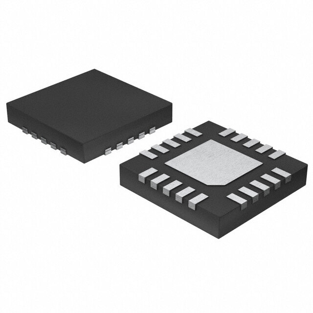
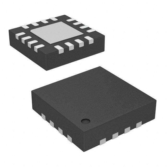
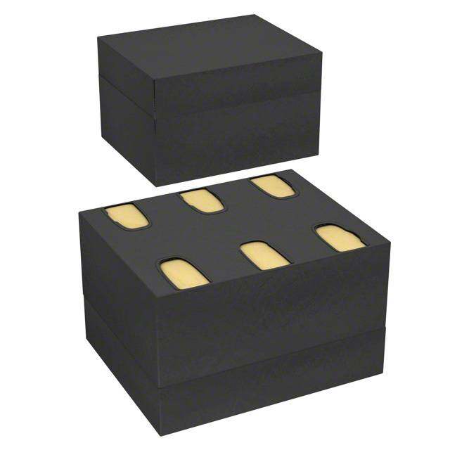
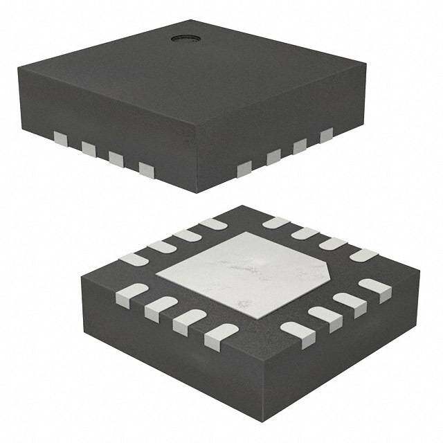
| 产品图片 |
|
| rohs | 符合RoHS无铅 / 符合限制有害物质指令(RoHS)规范要求 |
| 产品系列 | RF集成电路,RF 开关 IC,MACOM MA4SW210HMIC™ |
| 数据手册 | |
| P1dB | - |
| 产品型号 | MA4SW210MA4SW210 |
| RF类型 | 通用 |
| 产品种类 | RF 开关 IC |
| 介入损耗 | 0.7 dB |
| 供应商器件封装 | 模具 |
| 关闭隔离—典型值 | 42 dB |
| 其它名称 | 1465-1049 |
| 包装 | 散装 |
| 商标 | MACOM |
| 安装风格 | SMD/SMT |
| 封装/外壳 | 模具 |
| 封装/箱体 | HMIC Die |
| 工作温度 | -65°C ~ 125°C |
| 工厂包装数量 | 50 |
| 开关数量 | Single |
| 开关配置 | SPDT |
| 拓扑 | 反射 |
| 插损@频率 | 0.7dB @ 20GHz |
| 最大工作温度 | + 125 C |
| 最小工作温度 | - 65 C |
| 标准包装 | 50 |
| 特性 | - |
| 电压-电源 | - |
| 电源电流 | 20 mA |
| 电路 | SPDT |
| 阻抗 | - |
| 隔离@频率 | 42dB @ 20GHz (标准) |
| 频率 | 50 MHz to 20 GHz |
| 频率 -上 | 20GHz |
| 频率 -下 | 50MHz |


- 商务部:美国ITC正式对集成电路等产品启动337调查
- 曝三星4nm工艺存在良率问题 高通将骁龙8 Gen1或转产台积电
- 太阳诱电将投资9.5亿元在常州建新厂生产MLCC 预计2023年完工
- 英特尔发布欧洲新工厂建设计划 深化IDM 2.0 战略
- 台积电先进制程称霸业界 有大客户加持明年业绩稳了
- 达到5530亿美元!SIA预计今年全球半导体销售额将创下新高
- 英特尔拟将自动驾驶子公司Mobileye上市 估值或超500亿美元
- 三星加码芯片和SET,合并消费电子和移动部门,撤换高东真等 CEO
- 三星电子宣布重大人事变动 还合并消费电子和移动部门
- 海关总署:前11个月进口集成电路产品价值2.52万亿元 增长14.8%

PDF Datasheet 数据手册内容提取
MA4SWx10 Series HMIC™ Silicon PIN Diode Switches Rev. V11 Features Functional Diagrams Broad Bandwidth Specified from 50 MHz to 20 GHz Usable from 50 MHz to 26.5 GHz J1 J2 Lower Insertion Loss / Higher Isolation Fully Monolithic, Glass Encapsulated Chip Up to +33 dBm CW Power Handling @ +25°C RoHS* Compliant Description MA4SW110 (SPST) The MA4SW110 (SPST), MA4SW210 (SPDT) and MA4SW310 (SP3T) are series-shunt, broadband, PIN diode switches made with MACOM’s HMICTM (Heterolithic Microwave Integrated Circuit) process. This process allows the silicon pedestals which form the series - shunt diodes and vias to be embedded into low loss, low dispersion glass. By also J2 J3 incorporating small spacing between circuit elements, the result is an HMIC chip with low insertion loss and high isolation at frequencies up to 26.5 GHz. They are designed for use as moderate power, high J1 performance switches and provide superior performance when compared to similar designs that use discrete components. MA4SW210 (SPDT) The top side of the chip is protected by a polymer coating for manual or automatic handling and large gold bond pads help facilitate connection of low inductance ribbons. The gold metallization on the backside of the chip allows for attachment via 80/20, gold/tin solder or conductive silver epoxy. J3 J2 J4 Ordering Information Part Number Package J1 MA4SW110 Gel Pack MA4SW210 Gel Pack MA4SW310 (SP3T) MA4SW310 Gel Pack *Restrictions on Hazardous Substances, European Union Directive 2011/65/EU. 111 M/A-COM Technology Solutions Inc. (MACOM) and its affiliates reserve the right to make changes to the product(s) or information contained herein without notice. Visit www.macom.com for additional data sheets and product information. For further information and support please visit: https://www.macom.com/support
MA4SWx10 Series HMIC™ Silicon PIN Diode Switches Rev. V11 Electrical Specifications: T = 25°C, 20 mA A MA4SW110 (SPST) Parameter Test Conditions Units Min. Typ. Max. 6 GHz 0.4 0.7 Insertion Loss 13 GHz dB — 0.5 0.9 20 GHz 0.7 1.2 6 GHz 46 55 Isolation 13 GHz dB 39 47 — 20 GHz 34 42 6 GHz 22 31 Input Return Loss 13 GHz dB 15 33 — 20 GHz 14 27 Switching Speed1 — ns — 50 — Voltage Rating2 — V — — 50 Signal Compression 500 mW, 1 GHz dB — 0.2 — MA4SW210 (SPDT) Parameter Test Conditions Units Min. Typ. Max. 6 GHz 0.4 0.7 Insertion Loss 13 GHz dB — 0.5 1.0 20 GHz 0.7 1.2 6 GHz 48 63 Isolation 13 GHz dB 40 50 — 20 GHz 34 42 6 GHz 20 27 Input Return Loss 13 GHz dB 18 25 — 20 GHz 15 25 Switching Speed1 — ns — 50 — Voltage Rating2 — V — — 50 Signal Compression 500 mW, 1 GHz dB — 0.2 — MA4SW310 (SP3T) Parameter Test Conditions Units Min. Typ. Max. 6 GHz 0.5 0.8 Insertion Loss 13 GHz dB — 0.7 1.1 20 GHz 0.9 1.5 6 GHz 49 57 Isolation 13 GHz dB 42 48 — 20 GHz 33 42 6 GHz 20 24 Input Return Loss 13 GHz dB 14 22 — 20 GHz 11 21 Switching Speed1 — ns — 50 — Voltage Rating2 — V — — 50 Signal Compression 500 mW, 1 GHz dB — 0.2 — 1. Typical switching speed is measured from (10% to 90% and 90% to 10% of detected RF voltage), driven by TTL compatible drivers. In the modulating state, (the switching port is modulating, all other ports are in steady state isolation.) The switching speed is measured using an RC network using the following values: R = 50 - 200 Ω, C = 390 - 1000 pF. Driver spike current, I = C dv/dt, ratio of spike current to steady C state current, is typically 10:1. 222 2. Maximum reverse leakage current in either the shunt or series PIN diodes shall be 10 µA maximum at -50 volts. M/A-COM Technology Solutions Inc. (MACOM) and its affiliates reserve the right to make changes to the product(s) or information contained herein without notice. Visit www.macom.com for additional data sheets and product information. For further information and support please visit: https://www.macom.com/support
MA4SWx10 Series HMIC™ Silicon PIN Diode Switches Rev. V11 Absolute Maximum Ratings3,4,5 Parameter Absolute Maximum Handling Procedures RF CW Incident Power +33 dBm Please observe the following precautions to avoid Reverse Voltage -50 V damage: Bias Current per Port ±50 mA @ +25°C Static Sensitivity Operating Temperature -65°C to +125°C These electronic devices are sensitive to electrostatic discharge (ESD) and can be damaged Storage Temperature -65°C to +150°C by static electricity. Proper ESD control techniques should be used when handling these Class 0 Junction Temperature +175°C (HBM) and Class C1 (CDM).devices. 3. Exceeding any one or combination of these limits may cause permanent damage to this device. 4. MACOM does not recommend sustained operation near these survivability limits. 5. Maximum operating conditions for a combination of RF power, DC bias and temperature: +33 dBm CW @ 15 mA (per diode) +85°C. Typical Performance Curves @ 10 GHz: Insertion Loss vs. Bias Current Isolation vs. Bias Current -0.3 -46 MA4SW110 -0.4 -48 MA4SW210 MA4SW310 B) -0.5 B) -50 d d ( ( -0.6 MA4SW110 -52 MA4SW210 MA4SW310 -0.7 -54 0 10 20 30 40 50 0 10 20 30 40 50 Current (mA) Current (mA) Input Return Loss vs. Bias Current Output Return Loss vs. Bias Current -15 -15 MA4SW110 MA4SW110 -20 MA4SW210 -20 MA4SW210 MA4SW310 MA4SW310 B) -25 B) -25 d d ( ( -30 -30 -35 -35 0 10 20 30 40 50 0 10 20 30 40 50 Current (mA) Current (mA) 333 M/A-COM Technology Solutions Inc. (MACOM) and its affiliates reserve the right to make changes to the product(s) or information contained herein without notice. Visit www.macom.com for additional data sheets and product information. For further information and support please visit: https://www.macom.com/support
MA4SWx10 Series HMIC™ Silicon PIN Diode Switches Rev. V11 Typical Performance Curves @ T = +25°C, 20 mA Bias Current A MA4SW110 Return Loss vs. Frequency Insertion Loss vs. Frequency -10 -0.2 Input Return Loss -15 -0.4 Output Return Loss -20 -0.6 B) B) d d ( -25 ( -0.8 -30 -1.0 -35 -1.2 0 5 10 15 20 25 30 0 5 10 15 20 25 30 Frequency (GHz) Frequency (GHz) MA4SW210 Return Loss vs. Frequency Insertion Loss vs. Frequency -10 -0.2 Input Return Loss -15 -0.4 Output Return Loss -20 -0.6 B) B) d d ( -25 ( -0.8 -30 -1.0 -35 -1.2 0 5 10 15 20 25 30 0 5 10 15 20 25 30 Frequency (GHz) Frequency (GHz) MA4SW310 Return Loss vs. Frequency Insertion Loss vs. Frequency -10 -0.2 Input Return Loss -15 Output Return Loss -0.4 -20 -0.6 B) B) d d ( -25 ( -0.8 -30 -1.0 -35 -1.2 0 5 10 15 20 25 30 0 5 10 15 20 25 30 Frequency (GHz) Frequency (GHz) 444 M/A-COM Technology Solutions Inc. (MACOM) and its affiliates reserve the right to make changes to the product(s) or information contained herein without notice. Visit www.macom.com for additional data sheets and product information. For further information and support please visit: https://www.macom.com/support
MA4SWx10 Series HMIC™ Silicon PIN Diode Switches Rev. V11 Typical Performance Curves @ T = +25°C, 20 mA Bias Current A MA4SW110 Isolation vs. Frequency -30 -40 -50 B) d ( -60 -70 -80 0 5 10 15 20 25 30 Frequency (GHz) MA4SW210 Isolation vs. Frequency -30 -40 -50 B) d ( -60 -70 -80 0 5 10 15 20 25 30 Frequency (GHz) MA4SW310 Isolation vs. Frequency -30 -40 -50 B) d ( -60 -70 -80 0 5 10 15 20 25 30 Frequency (GHz) 555 M/A-COM Technology Solutions Inc. (MACOM) and its affiliates reserve the right to make changes to the product(s) or information contained herein without notice. Visit www.macom.com for additional data sheets and product information. For further information and support please visit: https://www.macom.com/support
MA4SWx10 Series HMIC™ Silicon PIN Diode Switches Rev. V11 Operation of MA4SW Series Switches Bias Connections6 The simultaneous application of a negative DC current to the low loss port and positive DC current J1 RFIN to the isolated port is required for proper operation of the MA4SW series of PIN switches. The backside 20 pF area of the die is the RF and DC ground return and the DC return is through the common Port J1. A 20 nH J2 Bias constant current source should be used to supply 100 Ω the DC control currents. The control voltages at 20 pF 20 nH 20 pF these points will not exceed ±1.5 volts for supply currents up to +50mA. In the low loss state, the se- J2 ries diode must be forward biased and the shunt Switch 20 pF RFOUT diode reverse biased. On all isolated ports, the shunt Chip diode is forward biased and the series diode is MA4SW110 (SPST) reverse biased. Driver Connections and Drivers J1 RFIN 20 pF MA4SW110 (SPST) J3 Bias 20 nH J2 Bias DC Control Current (mA) RF Output State 100 Ω J2 J1-J2 20 pF 20 nH 20 pF 20 nH 20 pF -20 low loss J3 J2 +20 Isolation RFOUT 20 pF Switch 20 pF RFOUT Chip Compatible MACOM Driver MADR-007097-000100 MA4SW210 (SPDT) MA4SW210 (SPDT) DC Control Current (mA) RF Output States J1 RFIN J2 J3 J1-J2 J1-J3 20 pF -20 +20 low loss Isolation J4 Bias 20 nH J2 Bias +20 -20 Isolation low loss 100 Ω 20 pF 20 nH 20 pF 20 nH 20 pF Compatible MACOM Driver MADR-007097-000100 J4 J2 MA4SW310 (SP3T) RFOUT 20 pF 20 pF RFOUT Switch Chip DC Control Current (mA) RF Output States J3Bias 20 nH J2 J3 J4 J1-J2 J1-J3 J1-J4 20 pF 20 pF -20 +20 +20 low loss Isolation Isolation J3 RFOUT +20 -20 +20 Isolation low loss Isolation MA4SW310 (SP3T) +20 +20 -20 Isolation Isolation low loss Compatible MACOM Driver MADR-009190-000100 6. RLC values are for an operation frequency of 2-18 GHz and bias current of ± 20 mA per port.. 666 M/A-COM Technology Solutions Inc. (MACOM) and its affiliates reserve the right to make changes to the product(s) or information contained herein without notice. Visit www.macom.com for additional data sheets and product information. For further information and support please visit: https://www.macom.com/support
MA4SWx10 Series HMIC™ Silicon PIN Diode Switches Rev. V11 Chip Outline Drawings7,8 MA4SW110 INCHES MM DIM MIN. MAX. MIN. MAX. A 0.014 0.018 0.35 0.45 B 0.025 0.029 0.64 0.74 C 0.008 Ref. 0.20 Ref. D 0.004 0.006 0.10 0.15 E 0.004 Ref. 0.10 Ref. F 0.003 Ref. 0.08 Ref. G 0.003 Ref. 0.08 Ref. H 0.020 Ref. 0.52 Ref. MA4SW210 INCHES MM DIM MIN. MAX. MIN. MAX. A 0.029 0.033 0.73 0.83 B 0.004 0.006 0.10 0.15 C 0.004 Ref. 0.10 Ref. D 0.005 Ref. 0.13 Ref. E 0.009 Ref. 0.23 Ref. F 0.023 Ref. 0.58 Ref. G 0.007 Ref. 0.17 Ref. H 0.004 Ref. 0.10 Ref. MA4SW310 INCHES MM DIM MIN. MAX. MIN. MAX. A 0.046 0.050 1.16 1.26 B 0.036 0.040 0.92 1.02 C 0.019 Ref. 0.48 Ref. D 0.014 Ref. 0.36 Ref. E 0.004 Ref. 0.10 Ref. F 0.005 Ref. 0.13 Ref. G 0.004 0.006 0.10 0.15 H 0.005 Ref. 0.12 Ref. J 0.004 Ref. 0.10 Ref. 7. Topside and backside metallization is gold, 2.5 µm thick typical. 8. Yellow areas indicate ribbon/wire bonding pads 777 M/A-COM Technology Solutions Inc. (MACOM) and its affiliates reserve the right to make changes to the product(s) or information contained herein without notice. Visit www.macom.com for additional data sheets and product information. For further information and support please visit: https://www.macom.com/support
MA4SWx10 Series HMIC™ Silicon PIN Diode Switches Rev. V11 Cleanliness Chip Mounting The chips should be handled in a clean environment HMIC switches have Ti-Pt-Au backside metallization free of dust and organic contamination. and can be mounted using a gold-tin eutectic solder or conductive epoxy. Mounting surface must be free Wire / Ribbon Bonding of contamination and flat. Thermo compression wedge bonding using 0.003” x Eutectic Die Attachment 0.00025” ribbon or 0.001” diameter gold wire is recommended. A work stage temperature of 80/20, gold-tin, solder is recommended. A re-flow 150°C - 200°C, tool tip temperature of 120°C - 150° oven or hot gas die bonder with a temperature and a downward force of 18 to 22 grams should be setting of 290°C is normally used to melt the solder. used. If ultrasonic energy is necessary, it should be The chip should not be exposed to temperatures adjusted to the minimum level required to achieve a greater than 320°C for more than 20 seconds. good bond. Excessive power or force will fracture Typically no more than three seconds at peak the silicon beneath the bond pad causing it to lift. temperature is required for attachment. RoHS RF bond wires and ribbons should be kept as short compliant solders may also be used but solders rich as possible for optimum RF performance. in tin should be avoided as they will scavenge the backside gold and/or cause gold embrittlement. Epoxy Die Attachment A minimum amount of epoxy, 1 - 2 mils thick, should be used to attach chip. A thin epoxy fillet should be visible around the outer perimeter of the chip after placement. Epoxy cure time is typically 1 hour at 150°C. 888 M/A-COM Technology Solutions Inc. (MACOM) and its affiliates reserve the right to make changes to the product(s) or information contained herein without notice. Visit www.macom.com for additional data sheets and product information. For further information and support please visit: https://www.macom.com/support
MA4SWx10 Series HMIC™ Silicon PIN Diode Switches Rev. V11 M/A-COM Technology Solutions Inc. All rights reserved. Information in this document is provided in connection with M/A-COM Technology Solutions Inc ("MACOM") products. These materials are provided by MACOM as a service to its customers and may be used for informational purposes only. Except as provided in MACOM's Terms and Conditions of Sale for such products or in any separate agreement related to this document, MACOM assumes no liability whatsoever. MACOM assumes no responsibility for errors or omissions in these materials. MACOM may make changes to specifications and product descriptions at any time, without notice. MACOM makes no commitment to update the information and shall have no responsibility whatsoever for conflicts or incompatibilities arising from future changes to its specifications and product descriptions. No license, express or implied, by estoppels or otherwise, to any intellectual property rights is granted by this document. THESE MATERIALS ARE PROVIDED "AS IS" WITHOUT WARRANTY OF ANY KIND, EITHER EXPRESS OR IMPLIED, RELATING TO SALE AND/OR USE OF MACOM PRODUCTS INCLUDING LIABILITY OR WARRANTIES RELATING TO FITNESS FOR A PARTICULAR PURPOSE, CONSEQUENTIAL OR INCIDENTAL DAMAGES, MERCHANTABILITY, OR INFRINGEMENT OF ANY PATENT, COPYRIGHT OR OTHER INTELLECTUAL PROPERTY RIGHT. MACOM FURTHER DOES NOT WARRANT THE ACCURACY OR COMPLETENESS OF THE INFORMATION, TEXT, GRAPHICS OR OTHER ITEMS CONTAINED WITHIN THESE MATERIALS. MACOM SHALL NOT BE LIABLE FOR ANY SPECIAL, INDIRECT, INCIDENTAL, OR CONSEQUENTIAL DAMAGES, INCLUDING WITHOUT LIMITATION, LOST REVENUES OR LOST PROFITS, WHICH MAY RESULT FROM THE USE OF THESE MATERIALS. MACOM products are not intended for use in medical, lifesaving or life sustaining applications. MACOM customers using or selling MACOM products for use in such applications do so at their own risk and agree to fully indemnify MACOM for any damages resulting from such improper use or sale. 999 M/A-COM Technology Solutions Inc. (MACOM) and its affiliates reserve the right to make changes to the product(s) or information contained herein without notice. Visit www.macom.com for additional data sheets and product information. For further information and support please visit: https://www.macom.com/support