ICGOO在线商城 > 射频/IF 和 RFID > RF 开关 > HMC245QS16E

 Datasheet下载
- 型号: HMC245QS16E
- 制造商: Hittite
- 库位|库存: xxxx|xxxx
- 要求:
| 数量阶梯 | 香港交货 | 国内含税 |
| +xxxx | $xxxx | ¥xxxx |
查看当月历史价格
查看今年历史价格
HMC245QS16E产品简介:
ICGOO电子元器件商城为您提供HMC245QS16E由Hittite设计生产,在icgoo商城现货销售,并且可以通过原厂、代理商等渠道进行代购。 HMC245QS16E价格参考¥43.50-¥52.21。HittiteHMC245QS16E封装/规格:RF 开关, RF Switch IC General Purpose SP3T 3.5GHz 50Ohm 16-QSOP。您可以下载HMC245QS16E参考资料、Datasheet数据手册功能说明书,资料中有HMC245QS16E 详细功能的应用电路图电压和使用方法及教程。
HMC245QS16E是Analog Devices Inc.(亚德诺半导体)推出的一款高性能GaAs MMIC射频开关,属于RF开关类别。该器件采用16引脚QSOP封装,工作频率范围覆盖DC至4 GHz,适用于需要高频信号切换的多种射频系统。

其主要应用场景包括:通信基础设施中的基站收发信台(BTS)、软件定义无线电(SDR)、雷达系统、测试与测量设备以及工业和军事领域的射频信号路由。HMC245QS16E为单刀双掷(SPDT)开关,具有低插入损耗(典型值0.7 dB)、高隔离度(在4 GHz时优于35 dB)和快速切换速度(上升/下降时间约10 ns),能够实现高效、可靠的射频信号控制。

此外,该器件支持负电压控制逻辑,兼容+5V电源供电,适合在需要稳定性和抗干扰能力较强的环境中使用。由于其优异的线性性能(高P1dB和IP3),也广泛应用于对信号完整性要求较高的宽带通信系统中。

综上,HMC245QS16E凭借宽频带、低损耗、高隔离和快速响应等优势,成为无线通信、国防电子和高端仪器仪表中关键的射频前端组件。
| 参数 | 数值 |
| 产品目录 | |
| 描述 | IC MMIC GAAS SW SP3T 16QSOP |
| 产品分类 | |
| IIP3 | 44dBm (标准) |
| 品牌 | Hittite Microwave Corporation |
| 数据手册 | |
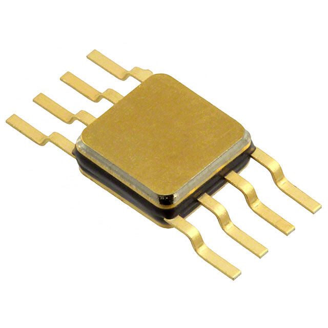
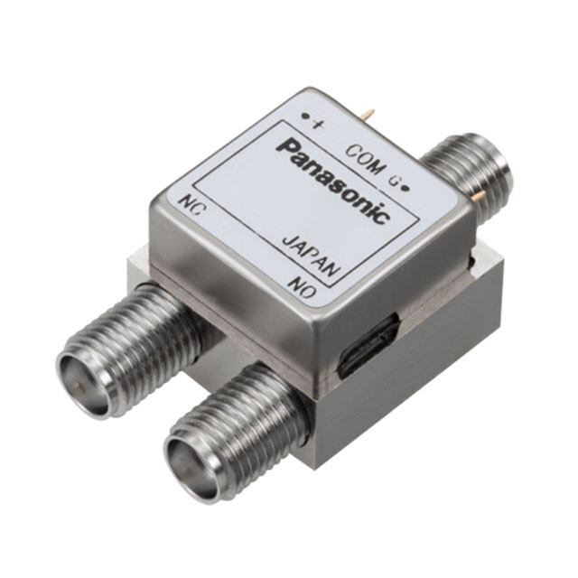
| 产品图片 |
|
| P1dB | 25dBm (标准) IP1dB |
| 产品型号 | HMC245QS16E |
| RF类型 | 通用 |
| rohs | 无铅 / 符合限制有害物质指令(RoHS)规范要求 |
| 产品系列 | - |
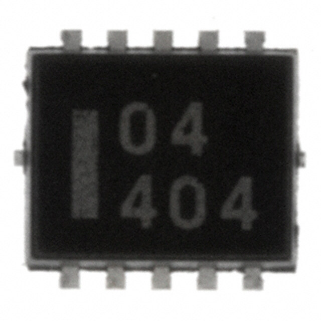
| 供应商器件封装 | 16-QSOP |
| 其它名称 | 1127-1010-1 |
| 包装 | 剪切带 (CT) |
| 封装/外壳 | 16-SSOP(0.154",3.90mm 宽) |
| 工作温度 | -40°C ~ 85°C |
| 拓扑 | 吸收性 |
| 插损@频率 | 0.7dB @ 3.5GHz |
| 标准包装 | 1 |
| 特性 | - |
| 电压-电源 | 5V |
| 电路 | SP3T |
| 阻抗 | 50 欧姆 |
| 隔离@频率 | 30dB @ 3.5GHz (标准) |
| 频率 -上 | 3.5GHz |
| 频率 -下 | DC |


- 商务部:美国ITC正式对集成电路等产品启动337调查
- 曝三星4nm工艺存在良率问题 高通将骁龙8 Gen1或转产台积电
- 太阳诱电将投资9.5亿元在常州建新厂生产MLCC 预计2023年完工
- 英特尔发布欧洲新工厂建设计划 深化IDM 2.0 战略
- 台积电先进制程称霸业界 有大客户加持明年业绩稳了
- 达到5530亿美元!SIA预计今年全球半导体销售额将创下新高
- 英特尔拟将自动驾驶子公司Mobileye上市 估值或超500亿美元
- 三星加码芯片和SET,合并消费电子和移动部门,撤换高东真等 CEO
- 三星电子宣布重大人事变动 还合并消费电子和移动部门
- 海关总署:前11个月进口集成电路产品价值2.52万亿元 增长14.8%


PDF Datasheet 数据手册内容提取
HMC245AQS16 / 245AQS16E v00.1213 GaAs MMIC SP3T Non-REFLECTIVE SWITCH, DC - 3.5 GHz Typical Applications Features The HMC245AQS16 / 245AQS16E is ideal for: Low Insertion Loss: 0.7 dB @ 2.0 GHz T • Basestation Infrastructure Non-Reflective Design M • CATV / DBS Integrated 2:3 TTL Decoder S • Wireless Local Loop “All Off” Isolation State - W • Test Equipment Single Positive Supply: Vdd = +5V O 16 Lead QSOP SMT Package R H Functional Diagram General Description T - I The HMC245AQS16 & HMC245AQS16E are low cost T L non-reflective SP3T switches in 16-lead QSOP sur- U face mount packages. Covering DC to 3.5 GHz, the M switch offers 30 to 40 dB isolation and a low inser- tion loss of 0.7 dB. A 2:3 TTL/CMOS compatible - S decoder is integrated on the switch requiring only 2 E control lines and a single +5V bias to select each path, H replacing 6 control lines normally required by GaAs C SP3T switches. T I W S Electrical Specifications, T = +25° C, For TTL Control and Vdd= +5V in a 50 Ohm System A Parameter Frequency Min. Typ. Max. Units DC - 2.0 GHz 0.7 1.0 dB Insertion Loss DC - 3.0 GHz 0.8 1.3 dB DC - 3.5 GHz 1.1 1.5 dB DC - 1.0 GHz 40 46 dB DC - 2.0 GHz 35 42 dB Isolation DC - 2.5 GHz 31 40 dB DC - 3.5 GHz 26 32 dB DC - 1.5 GHz 23 dB Return Loss “On State” DC - 3.5 GHz 17 dB 0.3 - 3.5 GHz 12 dB Return Loss RF1 - 3 “Off State” 0.5 - 3.5 GHz 15 dB 0.3 - 2.5 GHz 26 29 Input Power for 1 dB Compression dBm 0.3 - 3.5 GHz 25 28 Input Third Order Intercept 0.3 - 2.5 GHz 44 48 dBm (Two-tone Input Power = +10 dBm each tone) 0.3 - 3.5 GHz 40 44 Switching Characteristics tRISE, tFALL (10/90% RF) 0.3 - 3.5 GHz 40 ns tON, tOFF (50% CTL to 10/90% RF) 150 ns InfoFrmoart iopn rfiucrneis,h edde blyi vAenraylo ga Dnedvic teos ips lbaelcieeve do rtod beer sac:c Huraittet iatned Mreliiacbrleo. wHoawveeve rC, noo rpoForar tpioricne,, 2d eElilviezrayb, aentdh tDo rpivlaec,e C ohrdeelrms: sAfonardlo,g MDeAv i0ce1s8, 2In4c., responsibility is assumed by Analog Devices for its use, nor for any infringements of patents or other One Technology Way, P.O. Box 9106, Norwood, MA 02062-9106 1 rliicgehntss eo fi sth girrda nptaerdti ebsy t himatp mlicaaPyt iorhenso uonlrt ofertoh:m e9r wit7sis 8ues -eu2.n dS5ep0re ca-inf3iyc 3aptia4otne3sn ts ou rb jpeFacttae tnoxt c:r hig9ahn7tgs 8eo wf- 2Aithn5oau0lot g-n 3oDti3ecve7i.c 3eNso . POhrodnee:r 7 O81n-3-2li9n-e4 7a0t0 w(cid:127) wOrwde.hr oitntliitnee. cato wmww.analog.com Trademarks and registered trademarks arAe tphep plriocpearttyi oof nth eSir urespppecotivret :o wPnehrso.ne: 978-250-3A3p4p3li c aotrio na Spuppsp@orht: iPtthitoen.ec: o1-m800-ANALOG-D
HMC245AQS16 / 245AQS16E v00.1213 GaAs MMIC SP3T Non-REFLECTIVE SWITCH, DC - 3.5 GHz Insertion Loss vs. Temperature Isolation 0 0 -0.5 -10 T dB) -20 M OSS ( -1 N (dB)-30 S ON L-1.5 ATIO-40 - SERTI -2 ISOL-50 W N I-2.5 -60 O R -3 -70 0 0.5 1 1.5 2 2.5 3 3.5 4 0 0.5 1 1.5 2 2.5 3 3.5 4 H FREQUENCY (GHz) FREQUENCY (GHz) T - +25C +85C -40C RF1 RF2 RF3 I T L U M Return Loss Off State Isolation 0 0 - S -5 -10 E RETURN LOSS (dB)----22115050 ISOLATION (dB)----54320000 WITCH -30 -60 S -35 -70 0 0.5 1 1.5 2 2.5 3 3.5 4 0 0.5 1 1.5 2 2.5 3 3.5 4 FREQUENCY (GHz) FREQUENCY (GHz) RRFFC1-3 "On" RF1-3 "Off" RF1 RF2 RF3 0.1 and 1 dB Input Compression Point Input Third Order Intercept Point 32 54 m) dB 30 52 T ( SION POIN 2268 P3 (dBm) 4580 ES T I 46 R U OMP 24 INP 44 C UT 22 42 P N I 20 40 0 0.5 1 1.5 2 2.5 3 3.5 4 0 0.5 1 1.5 2 2.5 3 3.5 4 FREQUENCY (GHz) FREQUENCY (GHz) 0.1 dB Compression Point 1 dB Compression Point InfoFrmoart iopn rfiucrneis,h edde blyi vAenraylo ga Dnedvic teos ips lbaelcieeve do rtod beer sac:c Huraittet iatned Mreliiacbrleo. wHoawveeve rC, noo rpoForar tpioricne,, 2d eElilviezrayb, aentdh tDo rpivlaec,e C ohrdeelrms: sAfonardlo,g MDeAv i0ce1s8, 2In4c., responsibility is assumed by Analog Devices for its use, nor for any infringements of patents or other One Technology Way, P.O. Box 9106, Norwood, MA 02062-9106 rights of third parties that maPy rhesounlt fero:m 9 it7s 8us-e2. S5p0ec-if3ic3ati4on3s s u b jeFcta tox c: h9an7g8e w-2ith5ou0t -n3oti3ce7. 3No POhrodnee:r 7 O81n-3-2li9n-e4 7a0t0 w(cid:127) wOrwde.hr oitntliitnee. cato wmww.analog.com 2 license is granted by implication or otherwise under any patent or patent rights of Analog Devices. Trademarks and registered trademarks arAe tphep plriocpearttyi oof nth eSir urespppecotivret :o wPnehrso.ne: 978-250-3A3p4p3li c aotrio na Spuppsp@orht: iPtthitoen.ec: o1-m800-ANALOG-D
HMC245AQS16 / 245AQS16E v00.1213 GaAs MMIC SP3T Non-REFLECTIVE SWITCH, DC - 3.5 GHz Bias Voltage & Current Truth Table Vdd Range= +5 Vdc ±10% Control Input Signal Path State T Vdd (Vdc) Idd (Typ) (mA) Idd (Max) (mA) A B RF COM to: M +5 2.2 6.0 Low Low RF1 S High Low RF2 - TTL/CMOS Control Voltages Low High RF3 W High High All Off State Bias Condition O Low 0 to +0.8 Vdc @ 0.2 µA Typ. R High +2.0 to +5 Vdc @ 35 µA Typ. H T - I T L U M - S E H C T I W S InfoFrmoart iopn rfiucrneis,h edde blyi vAenraylo ga Dnedvic teos ips lbaelcieeve do rtod beer sac:c Huraittet iatned Mreliiacbrleo. wHoawveeve rC, noo rpoForar tpioricne,, 2d eElilviezrayb, aentdh tDo rpivlaec,e C ohrdeelrms: sAfonardlo,g MDeAv i0ce1s8, 2In4c., responsibility is assumed by Analog Devices for its use, nor for any infringements of patents or other One Technology Way, P.O. Box 9106, Norwood, MA 02062-9106 3 rliicgehntss eo fi sth girrda nptaerdti ebsy t himatp mlicaaPyt iorhenso uonlrt ofertoh:m e9r wit7sis 8ues -eu2.n dS5ep0re ca-inf3iyc 3aptia4otne3sn ts ou rb jpeFacttae tnoxt c:r hig9ahn7tgs 8eo wf- 2Aithn5oau0lot g-n 3oDti3ecve7i.c 3eNso . POhrodnee:r 7 O81n-3-2li9n-e4 7a0t0 w(cid:127) wOrwde.hr oitntliitnee. cato wmww.analog.com Trademarks and registered trademarks arAe tphep plriocpearttyi oof nth eSir urespppecotivret :o wPnehrso.ne: 978-250-3A3p4p3li c aotrio na Spuppsp@orht: iPtthitoen.ec: o1-m800-ANALOG-D
HMC245AQS16 / 245AQS16E v00.1213 GaAs MMIC SP3T Non-REFLECTIVE SWITCH, DC - 3.5 GHz Absolute Maximum Ratings Bias Voltage Range (Port Vdd) +7.0 Vdc ELECTROSTATIC SENSITIVE DEVICE Control Voltage Range (A & B) -0.5V to Vdd +1 Vdc T OBSERVE HANDLING PRECAUTIONS Channel Temperature 150 °C M Thermal Resistance S Insertion Loss Path 150 °C/W Terminated Path 297 °C/W - W Storage Temperature -65 to +150 °C Operating Temperature -40 to +85 °C O Maximum Input Power R Vdd = +5 Vdc H Insertion Loss Path +28.5 dBm Terminated Path +23.4 dBm T - ESD Sensitivity (HBM) Class 1A I T L Outline Drawing U M - S E H C T I W S NOTES: 1. LEADFRAME MATERIAL: COPPER ALLOY 2. DIMENSIONS ARE IN INCHES [MILLIMETERS]. 3. DIMENSION DOES NOT INCLUDE MOLDFLASH OF 0.15mm PER SIDE. 4. DIMENSION DOES NOT INCLUDE MOLDFLASH OF 0.25mm PER SIDE. 5. ALL GROUND LEADS MUST BE SOLDERED TO PCB RF GROUND. Package Information Part Number Package Body Material Leadframe Plating MSL Rating Package Marking [3] HMC245AQS16 Low Stress Injection Molded Plastic Silica Sn/Pb Solder MSL1 [1] HMC245A and Silicon Impregnated XXXX HMC245AQS16E RoHS-compliant Low Stress Injection Molded 100% Matte Tin MSL1 [2] HMC245A Plastic Silica and Silicon Impregnated XXXX [1] Max peak reflow temperature of 235 °C [2] Max peak reflow temperature of 260 °C [3] 4-Digit lot number XXXX InfoFrmoart iopn rfiucrneis,h edde blyi vAenraylo ga Dnedvic teos ips lbaelcieeve do rtod beer sac:c Huraittet iatned Mreliiacbrleo. wHoawveeve rC, noo rpoForar tpioricne,, 2d eElilviezrayb, aentdh tDo rpivlaec,e C ohrdeelrms: sAfonardlo,g MDeAv i0ce1s8, 2In4c., responsibility is assumed by Analog Devices for its use, nor for any infringements of patents or other One Technology Way, P.O. Box 9106, Norwood, MA 02062-9106 rights of third parties that maPy rhesounlt fero:m 9 it7s 8us-e2. S5p0ec-if3ic3ati4on3s s u b jeFcta tox c: h9an7g8e w-2ith5ou0t -n3oti3ce7. 3No POhrodnee:r 7 O81n-3-2li9n-e4 7a0t0 w(cid:127) wOrwde.hr oitntliitnee. cato wmww.analog.com 4 license is granted by implication or otherwise under any patent or patent rights of Analog Devices. Trademarks and registered trademarks arAe tphep plriocpearttyi oof nth eSir urespppecotivret :o wPnehrso.ne: 978-250-3A3p4p3li c aotrio na Spuppsp@orht: iPtthitoen.ec: o1-m800-ANALOG-D
HMC245AQS16 / 245AQS16E v00.1213 GaAs MMIC SP3T Non-REFLECTIVE SWITCH, DC - 3.5 GHz Pin Descriptions Pin Number Function Description Interface Schematic T RF3, RF2, This pin is DC coupled and matched to 50 Ohms. M 1, 6, 12, 14 RF1, RFC Blocking capacitors are required. S - 2 - 51, 57,, 1161, 13, GND This gprino umnuds tto b me acxoinmniezec tiesdo ltaot iPoCn.B RF W O 8 Vdd Supply Voltage +5 Vdc ±10% R H T 9 B See truth table and control voltage table. - I T L U 10 A See truth table and control voltage table. M - S E H C T I W S InfoFrmoart iopn rfiucrneis,h edde blyi vAenraylo ga Dnedvic teos ips lbaelcieeve do rtod beer sac:c Huraittet iatned Mreliiacbrleo. wHoawveeve rC, noo rpoForar tpioricne,, 2d eElilviezrayb, aentdh tDo rpivlaec,e C ohrdeelrms: sAfonardlo,g MDeAv i0ce1s8, 2In4c., responsibility is assumed by Analog Devices for its use, nor for any infringements of patents or other One Technology Way, P.O. Box 9106, Norwood, MA 02062-9106 5 rliicgehntss eo fi sth girrda nptaerdti ebsy t himatp mlicaaPyt iorhenso uonlrt ofertoh:m e9r wit7sis 8ues -eu2.n dS5ep0re ca-inf3iyc 3aptia4otne3sn ts ou rb jpeFacttae tnoxt c:r hig9ahn7tgs 8eo wf- 2Aithn5oau0lot g-n 3oDti3ecve7i.c 3eNso . POhrodnee:r 7 O81n-3-2li9n-e4 7a0t0 w(cid:127) wOrwde.hr oitntliitnee. cato wmww.analog.com Trademarks and registered trademarks arAe tphep plriocpearttyi oof nth eSir urespppecotivret :o wPnehrso.ne: 978-250-3A3p4p3li c aotrio na Spuppsp@orht: iPtthitoen.ec: o1-m800-ANALOG-D
HMC245AQS16 / 245AQS16E v00.1213 GaAs MMIC SP3T Non-REFLECTIVE SWITCH, DC - 3.5 GHz Evaluation PCB T M S - W O R H T - I T L U M - S E H C T I W S List of Materials for Evaluation PCB EV1HMC245AQS16 [1] The circuit board used in the application should Item Description be generated with proper RF circuit design tech- J1 - J4 PCB Mount SMA RF Connector niques. Signal lines at the RF port should have 50 J5 - J8 DC Pin ohm impedance and the package ground leads C1 - C4 100 pF Capacitor, 0402 Pkg. should be connected directly to the ground plane C5 10k pF Capacitor, 0603 Pkg. similar to that shown above. The evaluation circuit HMC245AQS16 / 245AQS16E U1 SP3T Switch board shown above is available from Hittite Micro- PCB [2] 106536 Evaluation PCB wave Corporation upon request. [1] Reference this number when ordering complete evaluation PCB [2] Circuit Board Material: Rogers 4350 InfoFrmoart iopn rfiucrneis,h edde blyi vAenraylo ga Dnedvic teos ips lbaelcieeve do rtod beer sac:c Huraittet iatned Mreliiacbrleo. wHoawveeve rC, noo rpoForar tpioricne,, 2d eElilviezrayb, aentdh tDo rpivlaec,e C ohrdeelrms: sAfonardlo,g MDeAv i0ce1s8, 2In4c., responsibility is assumed by Analog Devices for its use, nor for any infringements of patents or other One Technology Way, P.O. Box 9106, Norwood, MA 02062-9106 rights of third parties that maPy rhesounlt fero:m 9 it7s 8us-e2. S5p0ec-if3ic3ati4on3s s u b jeFcta tox c: h9an7g8e w-2ith5ou0t -n3oti3ce7. 3No POhrodnee:r 7 O81n-3-2li9n-e4 7a0t0 w(cid:127) wOrwde.hr oitntliitnee. cato wmww.analog.com 6 license is granted by implication or otherwise under any patent or patent rights of Analog Devices. Trademarks and registered trademarks arAe tphep plriocpearttyi oof nth eSir urespppecotivret :o wPnehrso.ne: 978-250-3A3p4p3li c aotrio na Spuppsp@orht: iPtthitoen.ec: o1-m800-ANALOG-D