ICGOO在线商城 > 射频/IF 和 RFID > RF 开关 > ADG919BRMZ
 Datasheet下载
- 型号: ADG919BRMZ
- 制造商: Analog
- 库位|库存: xxxx|xxxx
- 要求:
| 数量阶梯 | 香港交货 | 国内含税 |
| +xxxx | $xxxx | ¥xxxx |
查看当月历史价格
查看今年历史价格
ADG919BRMZ产品简介:
ICGOO电子元器件商城为您提供ADG919BRMZ由Analog设计生产,在icgoo商城现货销售,并且可以通过原厂、代理商等渠道进行代购。 ADG919BRMZ价格参考¥16.04-¥30.12。AnalogADG919BRMZ封装/规格:RF 开关, 射频开关 IC 通用 SPDT 2GHz 8-MSOP。您可以下载ADG919BRMZ参考资料、Datasheet数据手册功能说明书,资料中有ADG919BRMZ 详细功能的应用电路图电压和使用方法及教程。
ADG919BRMZ是由Analog Devices Inc.(亚德诺半导体)生产的一款RF(射频)开关,广泛应用于需要高性能射频信号切换的场景。以下是该型号的主要应用场景:

 1. 无线通信系统
ADG919BRMZ适用于各种无线通信设备,如蜂窝基站、Wi-Fi路由器和无线接入点等。它能够在不同的射频通道之间快速切换,确保信号传输的高效性和稳定性。其低插入损耗和高隔离度特性,使得它在多频段、多制式的无线通信系统中表现出色。

 2. 测试与测量设备
在测试与测量领域,ADG919BRMZ常用于频谱分析仪、网络分析仪和信号发生器等设备中。这些设备需要对不同频率的信号进行精确测量,而ADG919BRMZ能够提供可靠的射频信号路径切换,确保测量结果的准确性。此外,其低失真和线性度特性也使得它在高精度测试中具有优势。

 3. 雷达系统
ADG919BRMZ可以应用于雷达系统的发射和接收路径中,特别是在相控阵雷达中。它能够在多个天线单元之间快速切换,帮助实现波束成形和多目标跟踪功能。其快速切换时间和低功耗特性,使得它在雷达系统中具备较高的实用价值。

 4. 卫星通信
在卫星通信地面站中,ADG919BRMZ可用于天线控制系统,实现对不同卫星链路的快速切换。它能够处理高频段的射频信号,并保持较低的插入损耗和高隔离度,确保通信链路的稳定性和可靠性。

 5. 物联网(IoT)设备
随着物联网设备的普及,ADG919BRMZ也被应用于智能家居、智能城市等领域的无线传感器网络中。它可以在不同的无线协议(如Zigbee、LoRa等)之间进行切换,支持多协议共存,提升系统的灵活性和兼容性。

 总结
ADG919BRMZ凭借其优异的射频性能、快速切换能力和低功耗特性,广泛应用于无线通信、测试与测量、雷达系统、卫星通信和物联网等领域。它为各类射频信号处理应用提供了可靠的解决方案,满足了现代电子系统对高性能射频开关的需求。
| 参数 | 数值 |
| 产品目录 | |
| 描述 | IC SW SPDT 2:1 REFL MUX 8-MSOPRF 开关 IC WB 43dB Iso 1GHz CMOS 2:1 Mux/SPDT |
| 产品分类 | |
| IIP3 | 36dBm (标准) |
| 品牌 | Analog Devices |
| 产品手册 | |
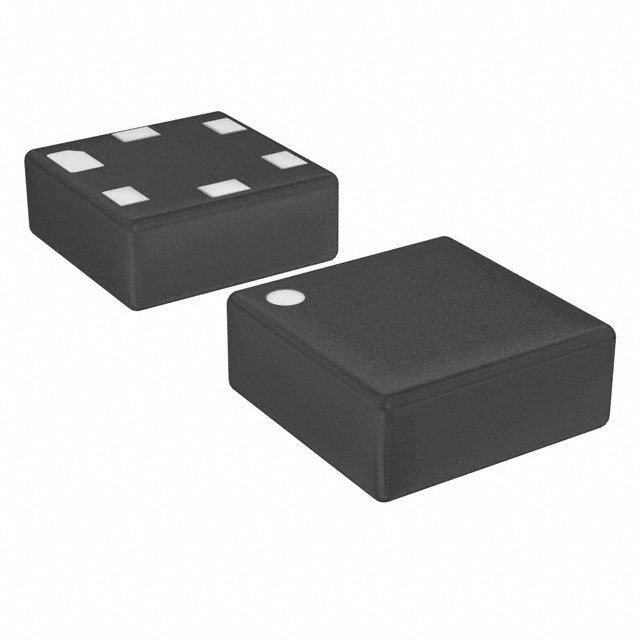
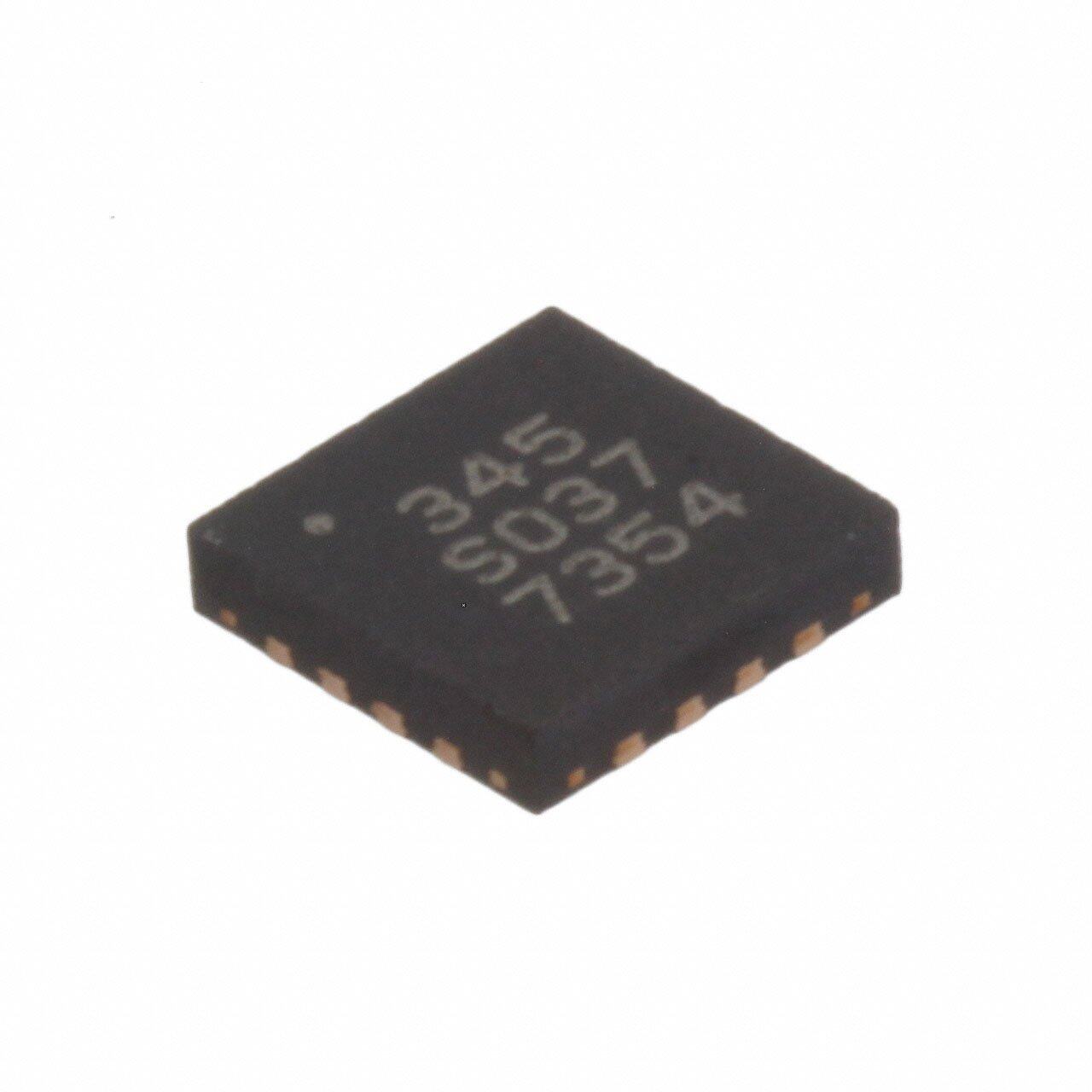
| 产品图片 |
|
| rohs | 符合RoHS无铅 / 符合限制有害物质指令(RoHS)规范要求 |
| 产品系列 | RF集成电路,RF 开关 IC,Analog Devices ADG919BRMZ- |
| 数据手册 | |
| P1dB | 17dBm (标准) P1dB |
| 产品型号 | ADG919BRMZ |
| RF类型 | 通用 |
| 产品培训模块 | http://www.digikey.cn/PTM/IndividualPTM.page?site=cn&lang=zhs&ptm=15131 |
| 产品目录页面 | |
| 产品种类 | RF 开关 IC |
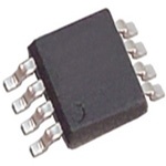
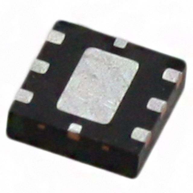
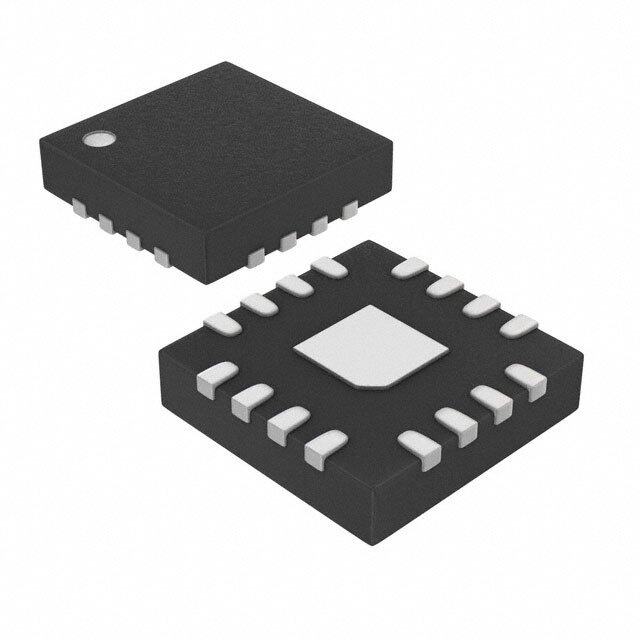
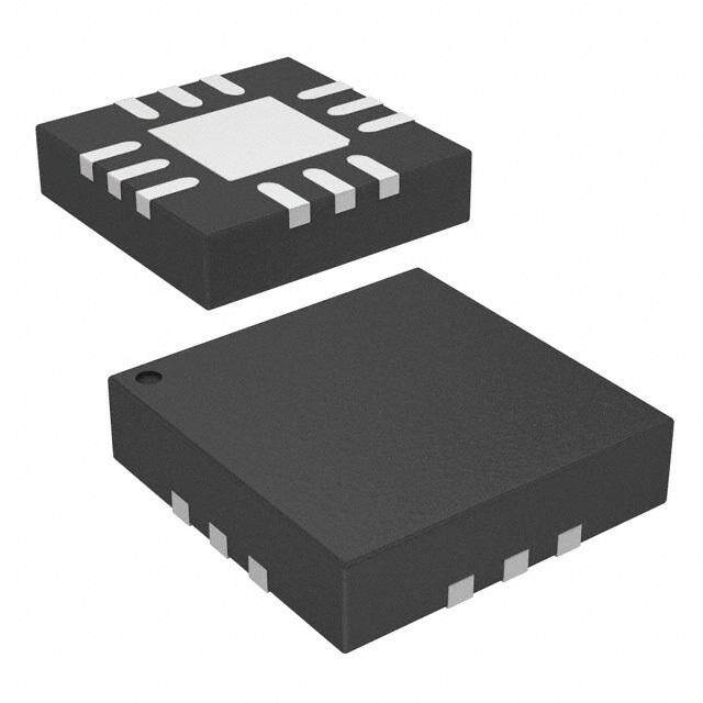
| 供应商器件封装 | 8-MSOP |
| 包装 | 管件 |
| 商标 | Analog Devices |
| 安装风格 | SMD/SMT |
| 封装 | Tube |
| 封装/外壳 | 8-TSSOP,8-MSOP(0.118",3.00mm 宽) |
| 封装/箱体 | MSOP-8 |
| 工作温度 | -40°C ~ 85°C |
| 工厂包装数量 | 50 |
| 开关数量 | Single |
| 开关配置 | SPDT |
| 拓扑 | 反射 |
| 插损@频率 | 0.8dB @ 1GHz |
| 最大功率耗散 | 2.5 uW |
| 最大工作温度 | + 85 C |
| 最小工作温度 | - 40 C |
| 标准包装 | 50 |
| 特性 | - |
| 电压-电源 | 1.65 V ~ 2.75 V |
| 电源电压-最大 | 2.75 V |
| 电源电压-最小 | V |
| 电路 | SPDT |
| 空闲时间—最大值 | 6.5 ns |
| 系列 | ADG919 |
| 视频文件 | http://www.digikey.cn/classic/video.aspx?PlayerID=1364138032001&width=640&height=505&videoID=2245193150001 |
| 运行时间—最大值 | 6.6 ns |
| 阻抗 | - |
| 隔离@频率 | 37dB @ 1GHz (标准) |
| 频率 -上 | 2GHz |
| 频率 -下 | DC |


- 商务部:美国ITC正式对集成电路等产品启动337调查
- 曝三星4nm工艺存在良率问题 高通将骁龙8 Gen1或转产台积电
- 太阳诱电将投资9.5亿元在常州建新厂生产MLCC 预计2023年完工
- 英特尔发布欧洲新工厂建设计划 深化IDM 2.0 战略
- 台积电先进制程称霸业界 有大客户加持明年业绩稳了
- 达到5530亿美元!SIA预计今年全球半导体销售额将创下新高
- 英特尔拟将自动驾驶子公司Mobileye上市 估值或超500亿美元
- 三星加码芯片和SET,合并消费电子和移动部门,撤换高东真等 CEO
- 三星电子宣布重大人事变动 还合并消费电子和移动部门
- 海关总署:前11个月进口集成电路产品价值2.52万亿元 增长14.8%


PDF Datasheet 数据手册内容提取
Wideband 4 GHz, 43 dB Isolation at 1 GHz, CMOS 1.65 V to 2.75 V, 2:1 Mux/SPDT Data Sheet ADG918/ADG919 FEATURES FUNCTIONAL BLOCK DIAGRAMS Wideband switch: −3 dB at 4 GHz ADG918 Absorptive/reflective switches RF1 High off isolation (43 dB at 1 GHz) Low insertion loss (0.8 dB at 1 GHz) RFC 50Ω Single 1.65 V to 2.75 V power supply RF2 CMOS/LVTTL control logic CTRL 8-lead MSOP and tiny 3 mm × 3 mm LFCSP 50Ω Low power consumption (<1 µA) APPLICATIONS ADG919 Wireless communications RF1 General-purpose RF switching Dual-band applications RFC High speed filter selection RF2 Digital transceiver front end switch CTRL ITFu snwerit mchoindgu les 03335-001 Antenna diversity switching Figure 2. GENERAL DESCRIPTION PRODUCT HIGHLIGHTS The ADG918/ADG919 are wideband switches using a CMOS 1. −43 dB off isolation at 1 GHz. process to provide high isolation and low insertion loss to 2. 0.8 dB insertion loss at 1 GHz. 1 GHz. The ADG918 is an absorptive (matched) switch having 3. Tiny 8-lead MSOP/LFCSP. 50 Ω terminated shunt legs, whereas the ADG919 is a reflective –0.4 switch. These devices are designed such that the isolation is –0.6 high over the dc to 1 GHz frequency range. They have on-board –0.8 CMOS control logic, thus eliminating the need for external –1.0 controlling circuitry. The control inputs are both CMOS and –1.2 B) LVTTL compatible. The low power consumption of these SS (d ––11..64 CMOS devices makes them ideally suited to wireless and O L –1.8 general-purpose high frequency switching applications. N O –2.0 TI 0 R –2.2 E VDD = 2.5V NS –2.4 –10 TA = 25°C I –2.6 –20 –2.8 VDD = 2.5V –30 –3.0 TA = 25°C ON (dB)–40 –3.210k 100k 1MFREQU1E0NMCY (Hz1)00M 1G 10G 03335-004 LATI–50 S12 Figure 3. Insertion Loss vs. Frequency O–60 S I –70 –80 S21 –90 –10010k 100k 1MFREQU1E0NMCY (Hz1)00M 1G 10G 03335-003 Figure 1. Off Isolation vs. Frequency Rev. E Document Feedback Information furnished by Analog Devices is believed to be accurate and reliable. However, no responsibility is assumed by Analog Devices for its use, nor for any infringements of patents or other One Technology Way, P.O. Box 9106, Norwood, MA 02062-9106, U.S.A. rights of third parties that may result from its use. Specifications subject to change without notice. No license is granted by implication or otherwise under any patent or patent rights of Analog Devices. Tel: 781.329.4700 ©2003–2016 Analog Devices, Inc. All rights reserved. Trademarks and registered trademarks are the property of their respective owners. Technical Support www.analog.com
ADG918/ADG919 Data Sheet TABLE OF CONTENTS Features .............................................................................................. 1 Terminology .................................................................................... 10 Applications ....................................................................................... 1 Test Circuits ..................................................................................... 11 Functional Block Diagrams ............................................................. 1 Applications Information .............................................................. 13 General Description ......................................................................... 1 Absorptive vs. Reflective Switch ............................................... 13 Product Highlights ........................................................................... 1 Wireless Metering....................................................................... 13 Revision History ............................................................................... 2 Tuner Modules ............................................................................ 13 Specifications ..................................................................................... 3 Filter Selection ............................................................................ 13 Absolute Maximum Ratings ............................................................ 5 ADG918/ADG919 Evaluation Board .......................................... 14 ESD Caution .................................................................................. 5 Outline Dimensions ....................................................................... 15 Pin Configuration and Function Descriptions ............................. 6 Ordering Guide .......................................................................... 16 Typical Performance Characteristics ............................................. 7 REVISION HISTORY 5/2016—Rev. D to Rev. E 8/2008—Rev. A to Rev. B Updated Outline Dimensions ....................................................... 15 Changes to Table 1, AC Electrical Characteristics, Third Order Intermodulation Intercept ................................................................ 3 3/2016—Rev. C to Rev. D Updated Outline Dimensions ....................................................... 15 Changed CP-8-2 to CP-8-13 ........................................ Throughout Changes to Ordering Guide .......................................................... 16 Changes to Figure 4 and Table 3 ..................................................... 6 Added Figure 5, Renumbered Sequentially .................................. 6 9/2004—Rev. 0 to Rev. A Changed ADG9xx Evaluation Board Section to ADG918/ Updated Format .................................................................. Universal ADG919 Evaluation Board Section ............................................. 14 Change to Data Sheet Title ............................................................... 1 Updated Outline Dimensions ....................................................... 15 Change to Features ............................................................................ 1 Changes to Ordering Guide .......................................................... 16 Change to Product Highlights ......................................................... 1 Changes to Specifications ................................................................. 3 9/08—Rev. B to Rev. C Change to ADG9xx Evaluation Board section ........................... 13 Changes to Ordering Guide .......................................................... 16 Changes to Ordering Guide .......................................................... 14 8/03—Revision 0: Initial Version Rev. E | Page 2 of 16
Data Sheet ADG918/ADG919 SPECIFICATIONS V = 1.65 V to 2.75 V, GND = 0 V, input power = 0 dBm, all specifications T to T , unless otherwise noted. Temperature range for DD MIN MAX B Version: −40°C to +85°C. Table 1. B Version Parameter Symbol Test Conditions/Comments Min Typ1 Max Unit AC ELECTRICAL CHARACTERISTICS Operating Frequency2 dc 2 GHz 3 dB Frequency3 4 GHz Input Power3 0 V dc bias 7 dBm 0.5 V dc bias 16 dBm Insertion Loss S , S DC to 100 MHz; V = 2.5 V ± 10% 0.4 0.7 dB 21 12 DD 500 MHz; V = 2.5 V ± 10% 0.5 0.8 dB DD 1000 MHz; V = 2.5 V ± 10% 0.8 1.25 dB DD Isolation—RFC to RF1/RF2 S , S 100 MHz 57 60 dB 21 12 (CP Package) 500 MHz 46 49 dB 1000 MHz 36 43 dB Isolation—RFC to RF1/RF2 S , S 100 MHz 55 60 dB 21 12 (RM Package) 500 MHz 43 47 dB 1000 MHz 34 37 dB Isolation—RF1 to RF2 (Crosstalk) S , S 100 MHz 55 58 21 12 (CP Package) 500 MHz 41 44 1000 MHz 31 37 Isolation—RF1 to RF2 (Crosstalk) S , S 100 MHz 54 57 21 12 (RM Package) 500 MHz 39 42 1000 MHz 31 33 Return Loss (On Channel)3 S , S DC to 100 MHz 21 27 dB 11 22 500 MHz 22 27 dB 1000 MHz 22 26 dB Return Loss (Off Channel)3 S , S DC to 100 MHz 18 23 dB 11 22 ADG918 500 MHz 17 21 dB 1000 MHz 16 20 dB On Switching Time3 t 50% CTRL to 90% RF 6.6 10 ns ON Off Switching Time3 t 50% CTRL to 10% RF 6.5 9.5 ns OFF Rise Time3 t 10% to 90% RF 6.1 9 ns RISE Fall Time3 t 90% to 10% RF 6.1 9 ns FALL 1 dB Compression3 P 1000 MHz 17 dBm –1 dB Third Order Intermodulation Intercept IP 900 MHz/901 MHz, 4 dBm 28.5 36 dBm 3 Video Feedthrough4 2.5 mV p-p DC ELECTRICAL CHARACTERISTICS Input High Voltage V V = 2.25 V to 2.75 V 1.7 V INH DD V V = 1.65 V to 1.95 V 0.65 V V INH DD CC Input Low Voltage V V = 2.25 V to 2.75 V 0.7 V INL DD V V = 1.65 V to 1.95 V 0.35 V V INL DD CC Input Leakage Current I 0 V ≤ V ≤ 2.75 V ± 0.1 ± 1 µA I IN Rev. E | Page 3 of 16
ADG918/ADG919 Data Sheet B Version Parameter Symbol Test Conditions/Comments Min Typ1 Max Unit CAPACITANCE3 RF On Capacitance C ON f = 1 MHz 1.6 pF RF CTRL Input Capacitance C f = 1 MHz 2 pF CTRL POWER REQUIREMENTS V 1.65 2.75 V DD Quiescent Power Supply Current I Digital inputs = 0 V or V 0.1 1 µA DD DD 1 Typical values are at VDD = 2.5 V and 25°C, unless otherwise stated. 2 Point at which insertion loss degrades by 1 dB. 3 Guaranteed by design, not subject to production test. 4 The dc transience at the output of any port of the switch when the control voltage is switched from high to low or low to high in a 50 Ω test setup, measured with 1 ns rise time pulses and 500 MHz bandwidth. Rev. E | Page 4 of 16
Data Sheet ADG918/ADG919 ABSOLUTE MAXIMUM RATINGS T = 25°C, unless otherwise noted. A Stresses at or above those listed under Absolute Maximum Ratings may cause permanent damage to the product. This is a Table 2. stress rating only; functional operation of the product at these Parameter Rating or any other conditions above those indicated in the operational V to GND −0.5 V to +4 V DD section of this specification is not implied. Operation beyond Inputs to GND −0.5 V to V + 0.3 V1 DD the maximum operating conditions for extended periods may Continuous Current 30 mA affect product reliability. Input Power 18 dBm Operating Temperature Range ESD CAUTION Industrial (B Version) −40°C to +85°C Storage Temperature Range −65°C to +150°C Junction Temperature 150°C θ Thermal Impedance JA MSOP 206°C/W LFCSP 2-Layer Board 84°C/W 4-Layer Board 48°C/W Lead Temperature, Soldering (10 sec) 300°C IR Reflow, Peak Temperature (<20 sec) 235°C ESD 1 kV 1RF1 and RF2 off port inputs to ground: −0.5 V to VDD – 0.5 V. Rev. E | Page 5 of 16
ADG918/ADG919 Data Sheet PIN CONFIGURATIONS AND FUNCTION DESCRIPTIONS VDD 1 8 RF1 VDD 1 8RF1 ADG918/ CTRL 2 ADG919 7 GND CTRL 2 ADG918/ 7GND GRNFCD 34 (NToOt Pto V SIEcaWle) 65 GRFN2D 03335-002 GRNFDC 34 (NAToODt PtGo V S9IEc1aW9le) 65GRFN2D N1.O PETAXEDPSO TSOE SDU PBASDT.R TAIET ET,H GEN EDX.POSED 03335-030 Figure 4. ADG918/ADG919 Pin Configuration (MSOP) Figure 5. ADG918/ADG919 Pin Configuration (LFCSP) Table 3. Pin Function Descriptions Pin No. MSOP LFCSP Mnemonic Function 1 1 V Power Supply Input. These devices can be operated from 1.65 V to 2.75 V; decouple V to GND. DD DD 2 2 CTRL Logic Control Input. See Table 4. 3, 6, 7 3, 6, 7 GND Ground Reference Point for All Circuitry on the Device. 4 4 RFC COMMON RF Port for Switch. 5 5 RF2 RF2 Port. 8 8 RF1 RF1 Port. Not applicable 0 EPAD Exposed Pad. Tie the exposed pad to substrate, GND. Table 4. Truth Table CTRL Signal Path 0 RF2 to RFC 1 RF1 to RFC Rev. E | Page 6 of 16
Data Sheet ADG918/ADG919 TYPICAL PERFORMANCE CHARACTERISTICS –0.2 –0.2 –0.4 –0.4 –40°C –0.6 –0.6 –0.8 VDD = 2.25V VDD = 2.5V VDD = 2.75V –0.8 +25°C +85°C –1.0 –1.0 INSERTION LOSS (dB)––––––––22211112........64286420 INSERTION LOSS (dB)––––––––11112222........86420642 –2.8 –2.8 –3.0 TA = 25°C –3.0 VDD = 2.5V –3.210k 100k 1MFREQU1E0NMCY (Hz1)00M 1G 10G 03335-017 –3.210k 100k 1MFREQU1E0NMCY (Hz1)00M 1G 10G03335-018 Figure 6. Insertion Loss vs. Frequency over Supplies Figure 9. Insertion Loss vs. Frequency over Temperature (RF1/RF2, S12, and S21) (RF1/RF2, S12, and S21) –0.30 0 –0.35 VDD = 2.75V –10 VTAD D= =2 51°.6C5VTO 2.75V –0.40 –20 dB) –0.45 LOSS ( –0.50 VDD = 2.25V VDD = 2.5V N (dB)––4300 N –0.55 O INSERTIO ––00..6650 ISOLATI––6500 S12 –0.70 –70 –0.75 TA = 25°C –80 S21 –0.8010k 100k 1MFREQU1E0NMCY (Hz1)00M 1G 10G03335-019 –9010k 100k 1MFREQU1E0NMCY (Hz1)00M 1G 10G 03335-020 Figure 7. Insertion Loss vs. Frequency over Supplies (RF1/RF2, Figure 10. Isolation vs. Frequency over Supplies (RF1/RF2, ADG918) S12, and S21) (Zoomed Figure 5 Plot) 0 –0.2 –0.4 –10 VDD = 1.65VTO 2.75V –0.6 TA = 25°C –0.8 VDD = 1.8V VDD= 1.65V VDD = 1.95V –20 –1.0 –30 B)–1.2 d S (–1.4 B) –40 S d N LO––11..86 ON ( –50 S12 NSERTIO–––222...420 ISOLATI ––7600 I –2.6 –80 ––23..80 TA = 25°C –90 S21 –3.210k 100k 1MFREQU1E0NMCY (Hz1)00M 1G 10G 03335-021 –10010k 100k 1MFREQU1E0NMCY (Hz1)00M 1G 10G 03335-022 Figure 8. Insertion Loss vs. Frequency over Supplies Figure 11. Isolation vs. Frequency over Supplies (RF1/RF2, ADG919) (RF1/RF2, S12, and S21) Rev. E | Page 7 of 16
ADG918/ADG919 Data Sheet –10 VDD = 2.5V –20 CH1 –30 –40 B) S12 (+85°C) N (d –50 O TI –60 CH2/3 LA S12 (+25°C) O S –70 I S12 (–40°C) –80 –90 S21 (–40°C, +25°C, +85°C) –100 10k 100k 1MFREQU1E0NMCY (Hz1)00M 1G 10G 03335-023 CCHH12 == CRTFR1 L= =1 010Vm/DVI/VDIV TTRFAISLEL == 66..11nnss 03335-024 CH3 = RF2 = 100mV/DIV Figure 12. Isolation vs. Frequency over Temperature (RF1/RF2, ADG919) Figure 15. Switch Timing 0 TA = 25°C –5 VDD = 2.5V –10 S (dB)–15 OFF SWITCH (ADG918) OS–20 CTRL L N R U–25 T RFC E R –30 ON SWITCH –35 –4100k 100k 1M FREQU10EMNCY (Hz1)00M 1G 10G 03335-026 CH1 500mV CH2 1mVΩ m 10.0nsC2.H0022 pm-pV 03335-027 Figure 13. Return Loss vs. Frequency (RF1/RF2, S11) Figure 16. Video Feedthrough –10 40 –15 TA = 25°C 35 –20 VDD = 2.5V –25 30 –30 B) –35 25 OSSTALK (d –––544050 IP(dBm)32105 R –55 C –60 10 –65 –70 5 VDD = 2.5V ––781500k 100k 1MFREQU1E0NMCY (Hz1)00M 1G 10G 03335-028 2050 350 450FREQU55E0NCY (M6H5z0) T7A5 =0 25°C 850 03335-029 Figure 14. Crosstalk vs. Frequency (RF1/RF2, S12, S21) Figure 17. IP3 vs. Frequency Rev. E | Page 8 of 16
Data Sheet ADG918/ADG919 20 18 16 14 m) 12 B (dB 10 d P–1 8 6 4 2 VDD = 2.5V TA = 25°C 00 250 500FREQUE7N50CY (MH1z0)00 1250 1500 03335-025 Figure 18. P−1 dB vs. Frequency Rev. E | Page 9 of 16
ADG918/ADG919 Data Sheet TERMINOLOGY t V FALL DD Fall time; time for the RF signal to fall from 90% to 10% of the Most positive power supply potential. on level. I DD Off Isolation Positive supply current. The attenuation between the input and output ports of the GND switch when the switch control voltage is in the off condition. Ground (0 V) reference. Insertion Loss CTRL The attenuation between the input and output ports of the Logic control input. switch when the switch control voltage is in the on condition. V INL P –1 dB Maximum input voltage for Logic 0. 1 dB compression point. The RF input power level at which the VINH switch insertion loss increases by 1 dB over the low level value. Minimum input voltage for Logic 1. It is a measure of how much power the on switch can handle before the insertion loss increases by 1 dB. I (I ) INL INH Input current of the digital input. IP 3 Third order intermodulation intercept. This is a measure of the C IN power in false tones that occur when closely spaced tones are Digital input capacitance. passed through a switch, whereby the nonlinearity of the switch t ON causes these false tones to be generated. Delay between applying the digital control input and the output Return Loss switching on. The amount of reflected power relative to the incident power at t OFF a port. Large return loss indicates good matching. By measuring Delay between applying the digital control input and the output return loss, the VSWR (voltage standing wave ratio) can be switching off. calculated from conversion charts. VSWR indicates the degree tRISE of matching present at a switch RF port. Rise time; time for the RF signal to rise from 10% to 90% of the Video Feedthrough on level. Spurious signals present at the RF ports of the switch when the control voltage is switched from high to low or low to high without an RF signal present. Rev. E | Page 10 of 16
Data Sheet ADG918/ADG919 TEST CIRCUITS Setups for the ADG918 are similar. VDD 0.1µF VOUT 0.1µF VDD VDD ADG919 5R0LΩ VDD RF1 50Ω NAENTAWLYOZREKR RFC RFC RFx VOUT 50% 50% VS CTRL 5R0LΩ VCTRL CTRL RF2 50Ω VS VOUT 90% 10% GND VCTRL GND tON tOFF 03335-009 INSERTION LOSS = 20logVOVUST 03335-012 Figure 19. Switch Timing: tON, tOFF Figure 22. Insertion Loss VDD 0.1µF VDD NETWORK 0.1µF VDD ADG919 ANALYZER VDD RFC RF1 50Ω VS RFC RFx VOUT 50% 50% 50Ω VS CTRL 5R0LΩ VCTRL10% 90% 90% 10% CTRL RF2 5R0LΩVOUT VOUT VCTRL GND GND tRISE tFALL 03335-010 CROSSTALK = 20logVOVUST 03335-013 Figure 20. Switch Figure 23. Crosstalk 0.1µF VDD VDD 0.1µF VDD ADG919 50Ω VS VDD ADG919 VOUT RF1 RL RF1 NC RFC 50Ω RFC OSCILLOSCOPE RF2 NETWORK NC CTRL 50Ω ANALYZER RF2 CTRL VCTRL GND VCTRL OFF ISOLATION = 20logVOVUST 03335-011 GND 03335-014 Figure 21. Off Isolation Figure 24. Video Feedthrough Rev. E | Page 11 of 16
ADG918/ADG919 Data Sheet VDD 0.1µF VDD 0.1µF VDD ADG919 VDD ADG919 RF1 50Ω RF RF1 50Ω SPECTRUM RFC SOURCE SPECTRUM RFC ANALYZER ANALYZER RF CTRL RF2 COMBINER CTRL RF2 SOURCE VS RF SOURCE VCTRL GND 03335-015 VCTRL GND 03335-016 Figure 25. IP3 Figure 26. P−1 dB Rev. E | Page 12 of 16
Data Sheet ADG918/ADG919 APPLICATIONS INFORMATION The ADG918/ADG919 are ideal solutions for low power, high The SPDT configuration isolates the high frequency receive frequency applications. The low insertion loss, high isolation signal from the high frequency transmit. between ports, low distortion, and low current consumption of these devices make them excellent solutions for many high LNA frequency switching applications. The most obvious application ANTENNA is in a transmit/receive block, as shown in the wireless metering ADG918 block diagram in Figure 27. Other applications include switching between high frequency TX/RX SWITCH PA 03335-005 filters, an ASK generator, an FSK generator, and an antenna Figure 27. Wireless Metering diversity switch in many tuner modules. TUNER MODULES ABSORPTIVE VS. REFLECTIVE SWITCH The ADG918 can be used in a tuner module to switch between The ADG918 is an absorptive (matched) switch with 50 Ω the cable TV input and the off-air antenna. This device is also terminated shunt legs, and the ADG919 is a reflective switch ideal for use as an antenna diversity switch, switching different with 0 Ω terminated shunts to ground. The ADG918 absorptive antenna to the tuner. switch has a good VSWR on each port, regardless of the switch mode. An absorptive switch must be used when there is a need VGA for a good VSWR that is looking into the port but not passing ftohree t hidreoaul gfho rs iagpnpalilc taot itohnes c tohmatm reoqnu piroer mt. Tinhime AumD Gre9f1le8c itsio tnhse re- ACNATBELNENA AADDGG991189/ TUNER 03335-006 back to the RF source. It also ensures that the maximum power Figure 28. Tuner Modules is transferred to the load. FILTER SELECTION The ADG919 reflective switch is suitable for applications where The ADG919 can be used as a 2:1 demultiplex to switch high high off port VSWR does not matter and the switch has some other frequency signals between different filters and also to multiplex desired performance feature. It can be used in many applications, the signal to the output. including high speed filter selection. In most cases, an absorptive switch can be used instead of a reflective switch, but not vice versa. WIRELESS METERING RFRINFCADG919 RRFF12 RRFF12 ADG919RFRCFOUT 03335-007 The ADG918 can be used in wireless metering applications. It Figure 29. Filter Selection can be used in conjunction with the ADF7020 transceiver IC for a utility metering transceiver application, providing the required isolation between the transmit and receive signals. Rev. E | Page 13 of 16
ADG918/ADG919 Data Sheet ADG918/ADG919 EVALUATION BOARD The ADG918/ADG919 evaluation board allows designers to evaluate the high performance wideband switches with a minimum of effort. In addition to the evaluation board, the user requires only a power supply and a network analyzer. An application note is available with the evaluation board and gives complete information about operating the evaluation board. The RFC port (see Figure 30) is connected through a 50 Ω transmission line to the top left SMA connector J1. RF1 and RF2 are connected through 50 Ω transmission lines to the top two SMA connectors, J2 and J3 respectively. A through trans- mPCisBsi oovne lri nthe ec oennvniercotnsm J4e nantadl cJ5o nadnidt ieosntsim baetinesg tehvea llousast eodf. the 03335-008 Figure 30. ADG918/ADG919 Evaluation Board Top View The board is constructed of a 4-layer, FR4 material with a dielectric constant of 4.3 and an overall thickness of 0.062 inches. Two ground layers with grounded planes provide ground for the RF transmission lines. The transmission lines were designed using a coplanar waveguide with ground plane model using a trace width of 0.052 inches, a clearance to ground plane of 0.030 inches, a dielectric thickness of 0.029 inches, and a metal thickness of 0.014 inches. Rev. E | Page 14 of 16
Data Sheet ADG918/ADG919 OUTLINE DIMENSIONS 3.20 3.00 2.80 8 5 5.15 3.20 4.90 3.00 4.65 2.80 1 4 PIN 1 IDENTIFIER 0.65 BSC 0.95 15° MAX 0.85 1.10 MAX 0.75 0.80 0.15 0.40 6° 0.23 0.55 CO0P.0L50A.1N0ARICTOYMPLIANT0. 2T5O JEDEC STA0°NDARDS 0M.0O9-187-AA 0.40 10-07-2009-B Figure 31. 8-Lead Mini Small Outline Package [MSOP] (RM-8) Dimensions shown in millimeters 1.84 3.10 1.74 3.00SQ 2.90 1.64 0.50BSC 5 8 PIN1INDEX EXPOSED 1.55 AREA PAD 1.45 0.50 1.35 0.40 0.30 4 1 PIN1 TOPVIEW BOTTOMVIEW INDICATOR (R0.15) 0.80 FORPROPERCONNECTIONOF 0.75 0.05MAX THEEXPOSEDPAD,REFERTO THEPINCONFIGURATIONAND 0.70 0.02NOM FUNCTIONDESCRIPTIONS COPLANARITY SECTIONOFTHISDATASHEET. SEATING 0.30 0.08 PLANE 0.25 0.203REF 0.C2O0MPLIANTTOJEDECSTANDARDSMO-229-WEED 12-07-2010-A Figure 32. 8-Lead Lead Frame Chip Scale Package [LFCSP] 3 mm × 3 mm Body and 0.75 mm Package Height (CP-8-13) Dimensions shown in millimeters Rev. E | Page 15 of 16
ADG918/ADG919 Data Sheet ORDERING GUIDE Model 1 Temperature Range Package Description Package Option Branding ADG918BRM –40°C to +85°C 8-Lead Mini Small Outline Package [MSOP] RM-8 W4B ADG918BRM-REEL7 –40°C to +85°C 8-Lead Mini Small Outline Package [MSOP] RM-8 W4B ADG918BRMZ –40°C to +85°C 8-Lead Mini Small Outline Package [MSOP] RM-8 W4B# ADG918BRMZ-500RL7 –40°C to +85°C 8-Lead Mini Small Outline Package [MSOP] RM-8 W4B# ADG918BRMZ-REEL –40°C to +85°C 8-Lead Mini Small Outline Package [MSOP] RM-8 W4B# ADG918BRMZ-REEL7 –40°C to +85°C 8-Lead Mini Small Outline Package [MSOP] RM-8 W4B# ADG918BCPZ-500RL7 –40°C to +85°C 8-Lead Lead Frame Chip Scale Package [LFCSP] CP-8-13 W4B# ADG918BCPZ-REEL7 –40°C to +85°C 8-Lead Lead Frame Chip Scale Package [LFCSP] CP-8-13 W4B# ADG919BRMZ –40°C to +85°C 8-Lead Mini Small Outline Package [MSOP] RM-8 S1X ADG919BRMZ-REEL7 –40°C to +85°C 8-Lead Mini Small Outline Package [MSOP] RM-8 S1X ADG919BCPZ-REEL7 –40°C to +85°C 8-Lead Lead Frame Chip Scale Package [LFCSP] CP-8-13 S1X EVAL-ADG918EBZ Evaluation Board EVAL-ADG919EBZ Evaluation Board 1 Z = RoHS Compliant Part, # denotes RoHS compliant product may be top or bottom marked. ©2003–2016 Analog Devices, Inc. All rights reserved. Trademarks and registered trademarks are the property of their respective owners. D03335-0-5/16(E) Rev. E | Page 16 of 16