ICGOO在线商城 > 射频/IF 和 RFID > RF 开关 > PE42442A-Z
 Datasheet下载
- 型号: PE42442A-Z
- 制造商: Peregrine
- 库位|库存: xxxx|xxxx
- 要求:
| 数量阶梯 | 香港交货 | 国内含税 |
| +xxxx | $xxxx | ¥xxxx |
查看当月历史价格
查看今年历史价格
PE42442A-Z产品简介:
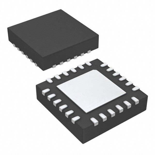
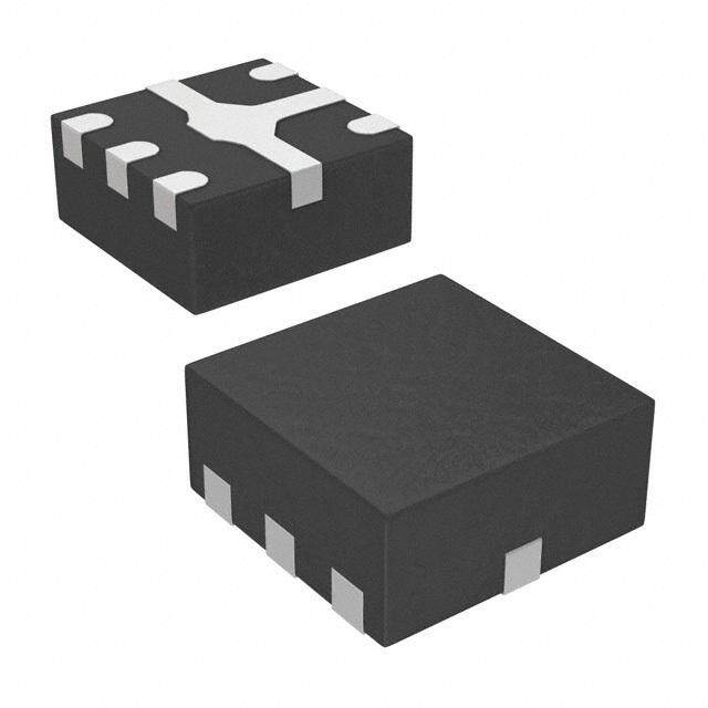
ICGOO电子元器件商城为您提供PE42442A-Z由Peregrine设计生产,在icgoo商城现货销售,并且可以通过原厂、代理商等渠道进行代购。 PE42442A-Z价格参考。PeregrinePE42442A-Z封装/规格:RF 开关, 射频开关 IC 3G/4G SP4T 6GHz 50 欧姆 24-QFN(4x4)。您可以下载PE42442A-Z参考资料、Datasheet数据手册功能说明书,资料中有PE42442A-Z 详细功能的应用电路图电压和使用方法及教程。
PE42442A-Z 是 pSemi 公司推出的一款射频(RF)开关,属于高性能单刀双掷(SPDT)开关。其主要应用场景包括:

1. 5G 和 4G 无线通信:
   PE42442A-Z 适用于蜂窝基站、小基站和用户设备中的射频信号切换。它支持高频段操作,适合用于毫米波和 Sub-6GHz 的 5G 应用,同时也能满足 4G LTE 网络的需求。

2. 物联网(IoT)设备:
   在低功耗物联网设备中,这款开关可以用于天线分集或频段切换,优化信号质量和能效表现。

3. 卫星通信与导航系统:
   该型号支持高线性度和低插入损耗的特性,使其成为卫星通信终端(如 VSAT 或 GNSS 接收器)的理想选择,用于信号路径切换。

4. 雷达和无人机技术:
   在雷达系统和无人机通信模块中,PE42442A-Z 可以实现快速高效的射频信号切换,确保系统的实时性和可靠性。

5. 测试与测量设备:
   这款开关可用于自动化测试设备(ATE)以及频谱分析仪等仪器中,提供稳定且精确的信号路由功能。

6. 工业无线通信:
   包括工业自动化、远程监控和其他需要高可靠射频性能的应用场景,PE42442A-Z 能够胜任复杂的工业环境要求。

总结来说,PE42442A-Z 凭借其卓越的射频性能、紧凑的设计和宽广的工作频率范围,在现代通信、航空航天、国防以及消费电子领域均具有广泛的应用价值。
| 参数 | 数值 |
| 产品目录 | |
| 描述 | IC RF SWITCH SP4T 24QFN |
| 产品分类 | |
| IIP3 | 58dBm (标准) |
| 品牌 | Peregrine Semiconductor |
| 数据手册 | |
| 产品图片 |
|
| P1dB | - |
| 产品型号 | PE42442A-Z |
| RF类型 | 3G/4G |
| rohs | 无铅 / 符合限制有害物质指令(RoHS)规范要求 |
| 产品系列 | UltraCMOS® |
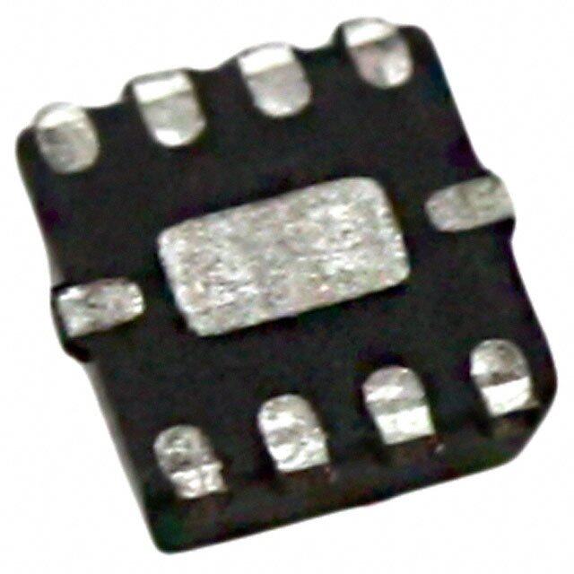
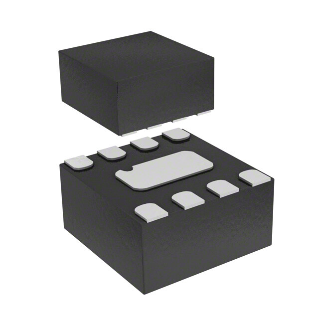
| 供应商器件封装 | 24-QFN(4x4) |
| 其它名称 | 1046-1096-1 |
| 包装 | 剪切带 (CT) |
| 封装/外壳 | 24-WFQFN 裸露焊盘 |
| 工作温度 | -40°C ~ 105°C |
| 拓扑 | 吸收性 |
| 插损@频率 | 1.1dB @ 900MHz |
| 标准包装 | 1 |
| 特性 | - |
| 电压-电源 | 3.3V |
| 电路 | SP4T |
| 配用 | /product-detail/zh/EK42442-01/1046-1095-ND/4747402 |
| 阻抗 | 50 欧姆 |
| 隔离@频率 | 61dB @ 900MHz(标准) |
| 频率 -上 | 6GHz |
| 频率 -下 | 30MHz |


- 商务部:美国ITC正式对集成电路等产品启动337调查
- 曝三星4nm工艺存在良率问题 高通将骁龙8 Gen1或转产台积电
- 太阳诱电将投资9.5亿元在常州建新厂生产MLCC 预计2023年完工
- 英特尔发布欧洲新工厂建设计划 深化IDM 2.0 战略
- 台积电先进制程称霸业界 有大客户加持明年业绩稳了
- 达到5530亿美元!SIA预计今年全球半导体销售额将创下新高
- 英特尔拟将自动驾驶子公司Mobileye上市 估值或超500亿美元
- 三星加码芯片和SET,合并消费电子和移动部门,撤换高东真等 CEO
- 三星电子宣布重大人事变动 还合并消费电子和移动部门
- 海关总署:前11个月进口集成电路产品价值2.52万亿元 增长14.8%


PDF Datasheet 数据手册内容提取
Product Specification PE42442 UltraCMOS® SP4T RF Switch 30 MHz–6 GHz Product Description Features The PE42442 is a HaRP™ technology-enhanced absorptive SP4T RF switch designed for use in 3G/4G Four symmetric, absorptive RF ports wireless infrastructure and other high performance RF High isolation applications. 61 dB @ 900 MHz This switch is a pin-compatible four throw version of the 55 dB @ 2100 MHz PE42451 with a wider frequency and power supply range. 52 dB @ 2700 MHz It is comprised of four symmetric RF ports with very high isolation up to 6 GHz. An integrated CMOS decoder 43 dB @ 4000 MHz facilitates a two- or three-pin 1.8V CMOS control 32 dB @ 6000 MHz interface. In addition, no external blocking capacitors are High linearity required if 0 VDC is present on the RF ports. IIP2 of 97 dBm The PE42442 is manufactured on Peregrine’s IIP3 of 58 dBm UltraCMOS® process, a patented variation of silicon-on- 1.8V control logic compatible insulator (SOI) technology on a sapphire substrate. 105 °C operating temperature Peregrine’s HaRP technology enhancements deliver high Fast switching time of 255 ns linearity and excellent harmonics performance. It is an Two- or three-pin CMOS logic control innovative feature of the UltraCMOS process, offering the External negative supply option performance of GaAs with the economy and integration of conventional CMOS. ESD performance 4 kV HBM on RF pins to GND 2 kV HBM on all pins Figure 1. Functional Diagram Figure 2. Package Type 24-lead 4 4 mm QFN DOC-59069 Document No. DOC-33414-7 │ www.psemi.com ©2013-2017 Peregrine Semiconductor Corp. All rights reserved. Page 1 of 11
PE42442 Product Specification Table 1. Electrical Specifications @ +25 °C (Z = Z = 50Ω) unless otherwise noted S L Normal mode1: V = 3.3V, V = 0V or Bypass mode2: V = 3.3V, V = –3.3V DD SS_EXT DD SS_EXT Parameter Path Condition Min Typ Max Unit Operating frequency 30 6000 MHz 450 MHz 0.85 1.00 dB 900 MHz 0.90 1.05 dB 2100 MHz 1.10 1.35 Insertion loss RFC–RFX dB 2700 MHz 1.15 1.40 dB 4000 MHz 1.25 1.50 dB 6000 MHz 1.90 2.35 450 MHz 62 67 dB 900 MHz 55 61 dB 2100 MHz 52 55 Isolation RFC–RFX dB 2700 MHz 50 52 dB 4000 MHz 42 43 dB 6000 MHz 27 32 450 MHz 61 65 dB 900 MHz 56 61 dB 2100 MHz 51 54 Isolation RFX–RFX dB 2700 MHz 50 52 dB 4000 MHz 41 44 dB 6000 MHz 29 32 30–4000 MHz 17 dB Return loss (active port) RFX 4000–6000 MHz 12 dB 30–4000 MHz 22 dB Return loss (terminated port) RFX 4000–6000 MHz 19 dB Input 0.1 dB compression point3 RFC–RFX 900 MHz 35 dBm Input IP2 RFC–RFX 1900 MHz 97 dBm Input IP3 RFC–RFX 1900 MHz 58 dBm Switching time 50% control to 90% or 10% RF 255 330 ns Notes: 1. Normal mode: single external positive supply used. 2. Bypass mode: both external positive supply and external negative supply used. 3. The input 0.1 dB compression point is a linearity figure of merit. Refer to Table 3 for the operating RF input power (50Ω). ©2013-2017 Peregrine Semiconductor Corp. All rights reserved. Document No. DOC-33414-7 │ UltraCMOS® RFIC Solutions Page 2 of 11
PE42442 Product Specification Figure 3. Pin Configuration (Top View) Table 3. Operating Ranges T Parameter Symbol Min Typ Max Unit D D C D EX GN GN RF GN Vss V3 Normal mode1 24 23 22 21 20 19 Supply voltage VDD 2.3 5.5 V Supply current I 110 µA DD Bypass mode2 Supply voltage V 2.7 5.5 V DD Supply current I 50 µA DD Negative supply V –3.6 –3.2 V voltage SS_EXT Normal or Bypass mode 7 8 9 10 11 12 Digital input high V 1.17 3.6 V D 3 D D 2 D (V1, V2, V3) IH N F N N F N G R G G R G Digital input low V –0.3 0.6 V (V1, V2, V3) IL Table 2. Pin Descriptions Digital input current3 I 1 µA CTRL Pin # Name Description RF input power, CW PMAX,CW 33 dBm RF input power into 1-3, 4, 6, 7, 9, P 24 dBm terminated ports, CW MAX,TERM 10, 12, 13, GND Ground 15, 21, 23, 24 Operating T –40 +105 °C 5 RF41 RF port 4 temperature range OP 8 RF31 RF port 3 Notes: 1. Normal mode: connect pin 20 to GND to enable internal negative voltage generator. 11 RF21 RF port 2 2. Bypass mode: apply a negative voltage to VSS_EXT (pin 20) to bypass and disable internal negative voltage generator. 14 RF11 RF port 1 3. The pull-down resistor in the EVK schematic may increase control current. 16 V Supply voltage DD 17 V1 Digital control logic input 1 Table 4. Absolute Maximum Ratings 18 V2 Digital control logic input 2 Parameter/Condition Symbol Min Max Unit 19 V32 Digital control logic input 3 Supply voltage V –0.3 5.5 V External Vss negative voltage control/ DD 20 V 3 SS_EXT ground Voltage on any DC input V –0.3 3.6 V I 22 RFC1 RF common Maximum input power P 34 dBm MAX_ABS Pad GND Exposed pad: Ground for proper operation Storage temperature range T –65 +150 °C Notes: 1. RF pins 5, 8, 11, 14 and 22 must be at 0 VDC. The RF pins do not ST require DC blocking capacitors for proper operation if the 0 VDC ESD voltage HBM1 requirement is met. All pins V 2.0 kV 2. Pin 19 must be grounded for 2-pin control, refer to Table 5A. ESD_HBM 3. Use VSS_EXT (pin 20, refer to Table 3) to bypass and disable internal RF pins to ground 4.0 kV enengaabtleiv ein vteorlntaagl en eggeanteivrea tvoor.l tCagoen ngeecnte VraSSto_Er.X T (pin 20, VSS_EXT = GND) to ESD voltage MM2, all pins VESD_MM 150 V ESD voltage CDM3, all pins V 250 V ESD_CDM Exceeding absolute maximum ratings may cause permanent damage. Operation should be Notes: 1. Human Body Model (MIL_STD 883 Method 3015) 2. Machine Model (JEDEC JESD22-A115) restricted to the limits in the Operating Ranges 3. Charged Device Model (JEDEC JESD22-C101D) table. Operation between operating range maximum and absolute maximum for extended periods may reduce reliability. Document No. DOC-33414-7 │www.psemi.com ©2013-2017 Peregrine Semiconductor Corp. All rights reserved. Page 3 of 11
PE42442 Product Specification Electrostatic Discharge (ESD) Precautions Table 5. Truth Table (3-pin control)* When handling this UltraCMOS device, observe Mode V3 V2 V1 the same precautions that you would use with Unsupported 0 0 0 other ESD-sensitive devices. Although this device RF1 on 0 0 1 contains circuitry to protect it from damage due to RF2 on 0 1 0 ESD, precautions should be taken to avoid exceeding the rating specified. RF3 on 0 1 1 RF4 on 1 0 0 Latch-Up Avoidance All off 1 0 1 Unlike conventional CMOS devices, UltraCMOS All off 1 1 0 devices are immune to latch-up. Unsupported 1 1 1 Note: * 3-pin control intended for legacy product support to PE42450 and Switching Frequency PE42451 or if All Off mode is required. Logic States 000 and 111 are unsupported and should not be used under any operating conditions. The PE42442 has a maximum 25 kHz switching rate in normal mode (pin 20 = GND). A faster Table 5A. Truth Table (2-pin control1)2 switching rate is available in bypass mode (pin 20 Mode V2 V1 = V ). The rate at which the PE42442 can be SS_EXT switched is then limited to the switching time as RF4 on 0 0 specified in Table 1. RF1 on 0 1 RF2 on 1 0 Switching frequency describes the time duration RF3 on 1 1 between switching events. Switching time is the time duration between the point the control signal Notes: 1. Pin 19 = V3 must be grounded. 2. 2-pin control is recommended for new product designs if All Off reaches 50% of the final value and the point the mode is not required. output signal reaches within 10% or 90% of its Optional External V Control (V ) target value. SS SS_EXT For applications the require a faster switching rate Moisture Sensitivity Level or spur-free performance, this part can be operated in bypass mode. Bypass mode requires The Moisture Sensitivity Level rating for the an external negative voltage in addition to an PE42442 in the 24-lead 4 4 mm QFN package external V supply voltage. is MSL1. DD As specified in Table 3, the external negative voltage (V ) when applied to pin 20 will SS_EXT disable and bypass the internal negative voltage generator. Spurious Performance The typical low-frequency spurious performance of the PE42442 in normal mode is –120 dBm (pin 20 = GND). If spur-free performance is desired, the internal negative voltage generator can be disabled by applying a negative voltage to V (pin 20). SS_EXT ©2013-2017 Peregrine Semiconductor Corp. All rights reserved. Document No. DOC-33414-7 │ UltraCMOS® RFIC Solutions Page 4 of 11
PE42442 Product Specification Typical Performance Data @ 25 °C and V = 3.3V unless otherwise noted DD Figure 4. Insertion Loss (All Paths) 0 −0.5 −1 B) d s ( s o L−1.5 n o erti s n I −2 −2.5 RF1 RF2 RF3 RF4 −3 0 1 2 3 4 5 6 Frequency (GHz) Figure 5. Insertion Loss vs Temp (RFC–RFX) Figure 6. Insertion Loss vs V (RFC–RFX) DD 0 0 −0.5 −0.5 −1 −1 B) B) d d oss ( oss ( n L−1.5 n L−1.5 o o erti erti ns ns I −2 I −2 −2.5 − 40 C −2.5 +25 C 2.3 V +85 C 3.3 V +105 C 5.5 V −3 −3 0 1 2 3 4 5 6 0 1 2 3 4 5 6 Frequency (GHz) Frequency (GHz) Document No. DOC-33414-7 │www.psemi.com ©2013-2017 Peregrine Semiconductor Corp. All rights reserved. Page 5 of 11
PE42442 Product Specification Typical Performance Data @ 25 °C and V = 3.3V unless otherwise noted DD Figure 7. Isolation vs Temp (RFC–RFX) Figure 8. Isolation vs V (RFC–RFX) DD 0 0 −10 −10 −20 −20 −30 −30 B) B) n (d−40 n (d−40 o o olati−50 olati−50 Is Is −60 −60 −70 −70 − 40 C +25 C 2.3 V −80 +85 C −80 3.3 V +105 C 5.5 V −90 −90 0 1 2 3 4 5 6 0 1 2 3 4 5 6 Frequency (GHz) Frequency (GHz) Figure 9. Isolation vs Temp (RFX–RFX) Figure 10. Isolation vs V (RFX–RFX) DD 0 0 −10 −10 −20 −20 −30 −30 B) B) n (d−40 n (d−40 o o olati−50 olati−50 Is Is −60 −60 −70 −70 − 40 C +25 C 2.3 V −80 +85 C −80 3.3 V +105 C 5.5 V −90 −90 0 1 2 3 4 5 6 0 1 2 3 4 5 6 Frequency (GHz) Frequency (GHz) ©2013-2017 Peregrine Semiconductor Corp. All rights reserved. Document No. DOC-33414-7 │ UltraCMOS® RFIC Solutions Page 6 of 11
PE42442 Product Specification Typical Performance Data @ 25 °C and V = 3.3V unless otherwise noted DD Figure 11. Active Port Return Loss vs Temp Figure 12. Active Port Return Loss vs V DD 0 0 −5 −5 −10 −10 B) B) d d s ( s ( s s Lo−15 Lo−15 n n ur ur et et R R −20 −20 −25 − 40 C −25 +25 C 2.3 V +85 C 3.3 V +105 C 5.5 V −30 −30 0 1 2 3 4 5 6 0 1 2 3 4 5 6 Frequency (GHz) Frequency (GHz) Figure 13. RFC Port Return Loss vs Temp Figure 14. RFC Port Return Loss vs V DD 0 0 −5 −5 −10 −10 B) B) d d Loss (−15 Loss (−15 n n ur ur et et R R −20 −20 −25 − 40 C −25 +25 C 2.3 V +85 C 3.3 V +105 C 5.5 V −30 −30 0 1 2 3 4 5 6 0 1 2 3 4 5 6 Frequency (GHz) Frequency (GHz) Figure 15. Return Loss (All Ports Terminated) Figure 16. IIP3 vs Frequency 0 70 −5 60 −10 50 −15 s (dB)−20 m) 40 eturn Los−−3205 IIP3(dB 30 R −35 20 RF1 −40 RF1 RF2 RF2 10 RF3 −45 RF3 RF4 RF4 −50 0 0 1 2 3 4 5 6 0 1 2 3 4 5 6 Frequency (GHz) Frequency (GHz) Document No. DOC-33414-7 │www.psemi.com ©2013-2017 Peregrine Semiconductor Corp. All rights reserved. Page 7 of 11
PE42442 Product Specification Evaluation Kit Figure 17. Evaluation Board Layout The SP4T switch Evaluation Board was designed to ease customer evaluation of Peregrine’s PE42442. The RF common port is connected through a 50Ω transmission line via the top SMA connector. RF1, RF2, RF3, and RF4 are connected through 50Ω transmission lines via side SMA connectors. A through 50Ω transmission is available via SMA connectors RFCAL1 and RFCAL2. This transmission line can be used to estimate the loss of the PCB over the environmental conditions being evaluated. The EVK board is constructed with four metal layers on dielectric materials of Rogers 4003C and 4450 with a total thickness of 32 mils. Layer 1 and layer 3 provide ground for the 50Ω transmission lines. The 50Ω transmission lines are designed in layer 2 for high isolation purpose and use a stripline waveguide design with a trace width of 9.4 mils and trace metal thickness of 1.8 mils. The board stack up for 50Ω transmission lines has 8 mil thickness of Rogers 4003C between layer 1 and layer 2, and 10 mil thickness of Rogers 4450 between layer 2 and layer 3. Please consult manufacturer's guidelines for proper board material properties in your application. The PCB should be designed in such a way that RF transmission lines and sensitive DC I/O traces such as V are heavily isolated SS_EXT from one another, otherwise the true performance of the PE42442 will not be yielded. DOC-59282 ©2013-2017 Peregrine Semiconductor Corp. All rights reserved. Document No. DOC-33414-7 │ UltraCMOS® RFIC Solutions Page 8 of 11
PE42442 Product Specification Figure 18. Evaluation Board Schematic DOC-33427 Document No. DOC-33414-7 │www.psemi.com ©2013-2017 Peregrine Semiconductor Corp. All rights reserved. Page 9 of 11
PE42442 Product Specification Figure 19. Package Drawing 24-lead 4 4 mm QFN 0.10 C A 4.00 (2X) 2.70±0.05 0.60 0.30 B 0.40±0.05(x24) (x24) 0.50 (x24) (x20) 0.50 13 18 (x20) 12 19 4.00 2.70±0.05 2.75 4.40 0.25±0.05 7 24 (x24) 0.10 C 6 1 Chamfer 0.30 x 45° (2X) 2.50 2.75 Ref. Pin #1 Corner 4.40 BOTTOM VIEW RECOMMENDED LAND PATTERN TOP VIEW DOC-58197 0.10 C 0.10 C A B 0.05 C 0.75±0.05 0.05 C ALL FEATURES SEATING PLANE 0.203 0.05 C Ref. SIDE VIEW Figure 20. Marking Specifications 42442 YYWW = Pin 1 designator ZZZZZ YYWW = Date code ZZZZZ = Las five digits of the lot number DOC-51207 ©2013-2017 Peregrine Semiconductor Corp. All rights reserved. Document No. DOC-33414-7 │ UltraCMOS® RFIC Solutions Page 10 of 11
PE42442 Product Specification Figure 21. Tape and Reel Drawing A = 4.35 0 B = 4.35 0 K = 1.1 0 Tape Feed Direction Pin 1 Top of Device Device Orientation in Tape Table 6. Ordering Information Ordering Code Description Package Shipping Method PE42442A-Z PE42442 SP4T RF switch Green 24-lead 4 4 mm QFN 3000 units/T&R EK42442-01 PE42442 Evaluation kit Evaluation kit 1/Box Sales Contact and Information For sales and contact information please visit www.psemi.com. Advance Information: The product is in a formative or design stage. The datasheet contains design target No patent rights or licenses to any circuits described in this datasheet are implied or granted to any third party. specifications for product development. Specifications and features may change in any manner without notice. Peregrine’s products are not designed or intended for use in devices or systems intended for surgical implant, Preliminary Specification: The datasheet contains preliminary data. Additional data may be added at a later or in other applications intended to support or sustain life, or in any application in which the failure of the date. Peregrine reserves the right to change specifications at any time without notice in order to supply the best Peregrine product could create a situation in which personal injury or death might occur. Peregrine assumes no possible product. Product Specification: The datasheet contains final data. In the event Peregrine decides to liability for damages, including consequential or incidental damages, arising out of the use of its products in change the specifications, Peregrine will notify customers of the intended changes by issuing a CNF (Customer such applications. Notification Form). The Peregrine name, logo, UltraCMOS and UTSi are registered trademarks and HaRP, MultiSwitch and DuNE The information in this datasheet is believed to be reliable. However, Peregrine assumes no liability for the use are trademarks of Peregrine Semiconductor Corp. Peregrine products are protected under one or more of the of this information. Use shall be entirely at the user’s own risk. following U.S. Patents: http://patents.psemi.com. Document No. DOC-33414-7 │www.psemi.com ©2013-2017 Peregrine Semiconductor Corp. All rights reserved. Page 11 of 11