ICGOO在线商城 > 射频/IF 和 RFID > RF 开关 > ADG936BRUZ-R
 Datasheet下载
- 型号: ADG936BRUZ-R
- 制造商: Analog
- 库位|库存: xxxx|xxxx
- 要求:
| 数量阶梯 | 香港交货 | 国内含税 |
| +xxxx | $xxxx | ¥xxxx |
查看当月历史价格
查看今年历史价格
ADG936BRUZ-R产品简介:
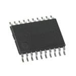
ICGOO电子元器件商城为您提供ADG936BRUZ-R由Analog设计生产,在icgoo商城现货销售,并且可以通过原厂、代理商等渠道进行代购。 ADG936BRUZ-R价格参考¥26.36-¥26.36。AnalogADG936BRUZ-R封装/规格:RF 开关, 射频开关 IC 通用 2 x SPDT 2GHz 50 欧姆 20-TSSOP。您可以下载ADG936BRUZ-R参考资料、Datasheet数据手册功能说明书,资料中有ADG936BRUZ-R 详细功能的应用电路图电压和使用方法及教程。
ADG936BRUZ-R 是由 Analog Devices Inc.(ADI)生产的一款 RF 开关,属于 ADG936 系列。该器件主要用于射频(RF)信号切换场景,具有低插入损耗、高隔离度和快速切换时间的特点,适用于多种无线通信和射频系统应用。

 应用场景:
1. 无线通信设备
   - 用于基站、中继器和小型蜂窝网络中的射频信号切换。
   - 支持多频段、多模式的无线通信系统,例如 LTE、5G NR 和 Wi-Fi。

2. 测试与测量仪器
   - 在频谱分析仪、矢量网络分析仪和其他射频测试设备中,用于切换不同的输入/输出通道。
   - 提供高精度和稳定的信号路径选择。

3. 雷达系统
   - 在军事或民用雷达中,用于天线波束切换或接收/发射信号的分离。
   - 满足高性能要求的射频信号路由需求。

4. 物联网(IoT)设备
   - 用于支持多频段或多协议的 IoT 设备,如 Zigbee、Bluetooth 和 LoRa。
   - 实现灵活的射频信号路径管理。

5. 卫星通信
   - 在卫星地面站或用户终端中,用于切换不同的射频链路。
   - 支持宽带和窄带信号的高效传输。

6. 医疗设备
   - 在超声波成像或射频消融设备中,用于信号路径的选择和优化。
   - 确保低噪声和高可靠性的射频信号处理。

7. 汽车电子
   - 在车载通信模块中,用于切换不同的射频天线或信号源。
   - 支持车联网(V2X)和 GPS 定位功能。

ADG936BRUZ-R 的典型工作频率范围为 DC 至 4 GHz,能够满足大多数射频应用的需求。其小型化的封装形式(RUG 封装)也使其非常适合空间受限的设计环境。此外,该器件的低功耗特性还适合电池供电的便携式设备。
| 参数 | 数值 |
| 产品目录 | |
| 描述 | IC SW DUAL SPDT REFLECT 20TSSOPRF 开关 IC WB 4GHz 36dB Iso CMOS Dual SPDT |
| 产品分类 | |
| IIP3 | 32dBm (标准) |
| 品牌 | Analog Devices Inc |
| 产品手册 | |
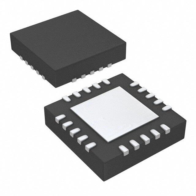
| 产品图片 |
|
| rohs | 符合RoHS无铅 / 符合限制有害物质指令(RoHS)规范要求 |
| 产品系列 | RF集成电路,RF 开关 IC,Analog Devices ADG936BRUZ-R- |
| 数据手册 | |
| P1dB | 16dBm (标准) P1dB |
| 产品型号 | ADG936BRUZ-R |
| RF类型 | 通用 |
| 产品培训模块 | http://www.digikey.cn/PTM/IndividualPTM.page?site=cn&lang=zhs&ptm=15131 |
| 产品目录页面 | |
| 产品种类 | RF 开关 IC |
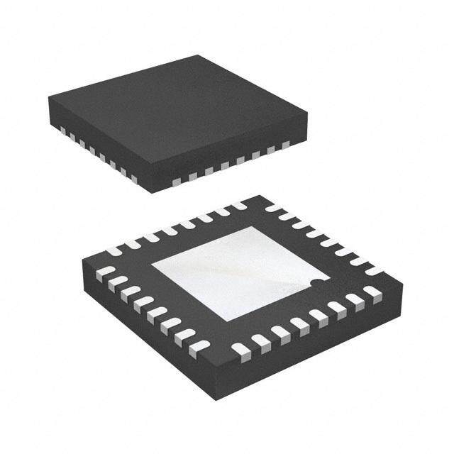
| 供应商器件封装 | 20-TSSOP |
| 其它名称 | ADG936BRUZR |
| 包装 | 管件 |
| 商标 | Analog Devices |
| 安装风格 | SMD/SMT |
| 封装 | Tube |
| 封装/外壳 | 20-TSSOP(0.173",4.40mm 宽) |
| 封装/箱体 | TSSOP-20 |
| 工作温度 | -40°C ~ 85°C |
| 工厂包装数量 | 75 |
| 开关数量 | Dual |
| 开关配置 | SPDT |
| 拓扑 | 反射 |
| 插损@频率 | 0.9dB @ 1GHz |
| 最大功率耗散 | 2.75 uW |
| 最大工作温度 | + 85 C |
| 最小工作温度 | - 40 C |
| 标准包装 | 75 |
| 特性 | - |
| 电压-电源 | 1.65 V ~ 2.75 V |
| 电源电压-最大 | 2.75 V |
| 电源电压-最小 | 0 V |
| 电路 | 2 x SPDT |
| 空闲时间—最大值 | 10 ns |
| 系列 | ADG936 |
| 视频文件 | http://www.digikey.cn/classic/video.aspx?PlayerID=1364138032001&width=640&height=505&videoID=2245193150001 |
| 运行时间—最大值 | 11 ns |
| 阻抗 | 50 欧姆 |
| 隔离@频率 | 36dB @ 1GHz (标准) |
| 频率 -上 | 2GHz |
| 频率 -下 | DC |


.jpg)


- 商务部:美国ITC正式对集成电路等产品启动337调查
- 曝三星4nm工艺存在良率问题 高通将骁龙8 Gen1或转产台积电
- 太阳诱电将投资9.5亿元在常州建新厂生产MLCC 预计2023年完工
- 英特尔发布欧洲新工厂建设计划 深化IDM 2.0 战略
- 台积电先进制程称霸业界 有大客户加持明年业绩稳了
- 达到5530亿美元!SIA预计今年全球半导体销售额将创下新高
- 英特尔拟将自动驾驶子公司Mobileye上市 估值或超500亿美元
- 三星加码芯片和SET,合并消费电子和移动部门,撤换高东真等 CEO
- 三星电子宣布重大人事变动 还合并消费电子和移动部门
- 海关总署:前11个月进口集成电路产品价值2.52万亿元 增长14.8%


PDF Datasheet 数据手册内容提取
Wideband 4 GHz, 36 dB Isolation at 1 GHz, CMOS, 1.65 V to 2.75 V, Dual SPDT Data Sheet ADG936/ADG936-R FEATURES FUNCTIONAL BLOCK DIAGRAMS Wideband switch: −3 dB @ 4 GHz ADG936 absorptive dual SPDT RF1A RF1A ADG936-R reflective dual SPDT RFCA RFCA High off isolation (36 dB @ 1 GHz) 50 Low insertion loss (0.9 dB dc to 1 GHz) RF2A RF2A Single 1.65 V to 2.75 V power supply INA INA CMOS/LVTTL control logic ADG936 50 ADG936-R 20-lead TSSOP and 4 mm × 4 mm LFCSP packages RF1B RF1B Low power consumption (1 μA maximum) RFCB RFCB APPLICATIONS 50 RF2B RF2B Wireless communications INB INB General-purpose RF switching DHiugahl- sbpaenedd a fpilptelirc saetlieocntsi on 50 04503-001 04503-012 Figure 1. Figure 2. Digital transceiver front end switch IF switching Tuner modules Antenna diversity switching GENERAL DESCRIPTION compatible. The low power consumption of these CMOS The ADG936/ADG936-R are wideband analog switches that devices makes them ideally suited for wireless applications and comprise two independently selectable SPDT switches using a general-purpose high frequency switching. CMOS process to provide high isolation and low insertion loss to 1 GHz. The ADG936 is an absorptive/matched dual SPDT PRODUCT HIGHLIGHTS with 50 Ω terminated shunt legs; the ADG936-R is a reflective 1. –36 dB off isolation @ 1 GHz. dual SPDT. These devices are designed such that the isolation is high over the dc to 1 GHz frequency range. They have on-board 2. 0.9 dB insertion loss @ 1 GHz. CMOS control logic, eliminating the need for external controlling circuitry. The control inputs are both CMOS and LVTTL 3. 20-lead TSSOP and 4 mm × 4 mm LFCSP packages. –10 –0.3 VDD = 2.5V ––00..45 TA = 25°C –0.6 –20 –0.7 –0.8 –0.9 –1.0 F ISOLATION (dB) –––345000 S21 ERTION LOSS (dB) –––––––––––11111111122...........12345678901 VDD= 2.5V OF –60 INS ––22..23 –2.4 –70 S12 ––22..56 –2.7 –2.8 –8010k 100k 1MFREQU1E0NMCY (Hz1)00M 1G 10G 04503-027 ––23..9010kTA = 251°0C0k 1MFREQU1E0NMCY (Hz1)00M 1G 10G 04503-015 Figure 3. Off Isolation vs. Frequency Figure 4. Insertion Loss vs. Frequency Rev. B Document Feedback Information furnished by Analog Devices is believed to be accurate and reliable. However, no responsibility is assumed by Analog Devices for its use, nor for any infringements of patents or other One Technology Way, P.O. Box 9106, Norwood, MA 02062-9106, U.S.A. rights of third parties that may result from its use. Specifications subject to change without notice. No license is granted by implication or otherwise under any patent or patent rights of Analog Devices. Tel: 781.329.4700 ©2004–2013 Analog Devices, Inc. All rights reserved. Trademarks and registered trademarks are the property of their respective owners. Technical Support www.analog.com
ADG936/ADG936-R Data Sheet TABLE OF CONTENTS Features .............................................................................................. 1 Typical Performance Characteristics ..............................................7 Applications ....................................................................................... 1 Test Circuits ........................................................................................9 Functional Block Diagrams ............................................................. 1 Applications ..................................................................................... 11 General Description ......................................................................... 1 Absorptive vs. Reflective ........................................................... 11 Product Highlights ........................................................................... 1 Filter Selection ............................................................................ 11 Revision History ............................................................................... 2 Tx/Rx Switching ......................................................................... 11 Specifications ..................................................................................... 3 Antenna Diversity Switch .......................................................... 11 Absolute Maximum Ratings ............................................................ 4 Evaluation Board ............................................................................ 12 ESD Caution .................................................................................. 4 Outline Dimensions ....................................................................... 13 Pin Configurations and Function Descriptions ........................... 5 Ordering Guide .......................................................................... 14 Terminology ...................................................................................... 6 REVISION HISTORY 4/13—Rev. A to Rev. B Changed CP-20-1 to CP-20-6 ........................................... Universal Added EPAD Note ............................................................................ 5 Updated Outline Dimensions ....................................................... 13 Changes to Ordering Guide .......................................................... 14 8/05—Rev. 0 to Rev. A Changes to Table 1 ............................................................................ 3 Changes to Figure 6 .......................................................................... 5 Changes to Ordering Guide .......................................................... 14 7/04—Revision 0: Initial Version Rev. B | Page 2 of 16
Data Sheet ADG936/ADG936-R SPECIFICATIONS V = 1.65 V to 2.75 V, GND = 0 V, input power = 0 dBm, all specifications T to T , unless otherwise noted.1 DD MIN MAX Table 1. B Version Parameter Symbol Conditions Min Typ2 Max Unit AC ELECTRICAL CHARACTERISTICS Operating Frequency3 DC 2 GHz 3 dB Frequency4 4 GHz Input Power4 0 V dc bias 7 dBm 0.5 V dc bias 16 dBm Insertion Loss S , S DC to 100 MHz; V = 2.5 V ± 10% 0.4 0.5 dB 21 12 DD 500 MHz; V = 2.5 V ± 10% 0.6 0.8 dB DD 1000 MHz; V = 2.5 V ± 10% 0.9 1.25 dB DD Isolation—RFCx to RF1x/RF2x S , S 100 MHz 52 60 dB 21 12 500 MHz 40 47 dB 1000 MHz 31 36 dB Crosstalk—RF1x to RF2x S , S 100 MHz 53 69 dB 21 12 500 MHz 42 45 dB 1000 MHz 34 37 dB Return Loss (On Channel)4 S , S DC to 100 MHz 20 25 dB 11 22 500 MHz 19 23 dB 1000 MHz 16 24 dB Return Loss (Off Channel)4 S , S DC to 100 MHz 18 24 dB 11 22 500 MHz 17 23 dB 1000 MHz 16 21 dB On Switching Time4 t 50% CTRL to 90% RF 11 14 ns ON Off Switching Time4 t 50% CTRL to 10% RF 10 13 ns OFF Rise Time4 t 10% to 90% RF 6.1 8 ns RISE Fall Time4 t 90% to 10% RF 6 8 ns FALL 1 dB Compression4 P 1000 MHz 16 dBm –1 dB Third-Order Intermodulation Intercept IP 900 MHz/901 MHz, 4 dBm 27.5 32 dBm 3 Video Feedthrough5 3 mV p-p DC ELECTRICAL CHARACTERISTICS Input High Voltage V V = 2.25 V to 2.75 V 1.7 V INH DD V V = 1.65 V to 1.95 V 0.65 V V INH DD CC Input Low Voltage V V = 2.25 V to 2.75 V 0.7 V INL DD V V = 1.65 V to 1.95 V 0.35 V V INL DD CC Input Leakage Current I 0 ≤ V ≤ 2.75 V ± 0.1 ± 1 µA I IN CAPACITANCE4 RF Port On Capacitance C ON f = 1 MHz 2.5 pF RF Digital Input Capacitance C f = 1 MHz 2 pF DIG POWER REQUIREMENTS V 1.65 2.75 V DD Quiescent Power Supply Current I Digital inputs = 0 V or V 0.1 1 µA DD DD 1 Temperature range of B Version: −40°C to +85°C. 2 Typical values are at VDD = 2.5 V and 25°C, unless otherwise noted. 3 Operating frequency is the point at which insertion loss degrades by 1 dB. 4 Guaranteed by design, not subject to production test. 5 Video feedthrough is the dc transience at the output of any port of the switch when the control voltage is switched from high to low or from low to high in a 50 Ω test setup, measured with 1 ns rise time pulses and a 500 MHz bandwidth. Rev. B | Page 3 of 16
ADG936/ADG936-R Data Sheet ABSOLUTE MAXIMUM RATINGS T = 25°C, unless otherwise noted. A Table 2. Stresses above those listed under Absolute Maximum Ratings Parameter Rating may cause permanent damage to the device. This is a stress V to GND –0.5 V to +4 V DD rating only; functional operation of the device at these or any Inputs to GND –0.5 V to V + 0.3 V1 DD other conditions above those indicated in the operational Continuous Current 30 mA section of this specification is not implied. Exposure to absolute Input Power 18 dBm maximum rating conditions for extended periods may affect Operating Temperature Range device reliability. Industrial (B Version) –40°C to +85°C Storage Temperature Range –65°C to +150°C Only one absolute maximum rating may be applied at any one Junction Temperature 150°C time. TSSOP Package θ Thermal Impedance 143°C/W JA LFCSP Package Table 3. Truth Table θ Thermal Impedance (4-Layer Board) 30.4°C/W JA INx RF1x RF2x Lead Temperature, Soldering (10 sec) 300°C 0 Off On IR Reflow, Peak Temperature (<20 sec) 235°C 1 On Off ESD 1 kV 1 RF1x/RF2x off port inputs to ground = –0.5 V to VDD – 0.5 V. ESD CAUTION ESD (electrostatic discharge) sensitive device. Electrostatic charges as high as 4000 V readily accumulate on the human body and test equipment and can discharge without detection. Although this product features proprietary ESD protection circuitry, permanent damage may occur on devices subjected to high energy electrostatic discharges. Therefore, proper ESD precautions are recommended to avoid performance degradation or loss of functionality. Rev. B | Page 4 of 16
Data Sheet ADG936/ADG936-R PIN CONFIGURATIONS AND FUNCTION DESCRIPTIONS A RFCA 1 20 GND DNGVDDCFRDNGANI 09876 21111 VDD 2 19 INA GND 3 ADG936 18 GND GND 1 15 GND RF1A 4 ADG936-R 17 RF2A RF1A 2 ADG936 14 RF2A GND 5 TOP VIEW 16 GND GND 3 ADG936-R 13 GND (Not to Scale) GND 4 TOP VIEW 12 GND GND 6 15 GND RF1B 5 (Not to Scale) 11 RF2B RF1B 7 14 RF2B GND 8 13 GND 678901 DDBDB GND 9 12 INB NNCNN RFCB 10 11 GND 04503-002 N1.O ETXEPSOSED PAGD TGIEFRD TGO SIUBSTATE, GND. 04503-003 Figure 5. 20-Lead TSSOP (RU-20) Figure 6. 20-Lead 4 mm × 4 mm LFCSP (CP-20-1) Table 4. Pin Function Descriptions Pin No. 20-Lead 20-Lead TSSOP LFCSP Mnemonic Description 1 18 RFCA Common RF Port for Switch A. 2 19 V Power Supply Input. These parts can operate from 1.65 V to 2.75 V. V should be decoupled DD DD to GND. 3, 5, 6, 8, 9, 1, 3, 4, 6, 7, GND Ground Reference Point for All Circuitry on the Part. 11, 13, 15, 9, 12, 13, 16, 18, 20 15, 17, 20 4 2 RF1A RF1A Port. 7 5 RF1B RF1B Port. 10 8 RFCB Common RF Port for Switch B. 12 10 INB Logic Control Input. 14 11 RF2B RF2B Port. 17 14 RF2A RF2A Port. 19 16 INA Logic Control Input. EP EP Exposed Pad. The exposed pad must be tied to substrate, GND. Rev. B | Page 5 of 16
ADG936/ADG936-R Data Sheet TERMINOLOGY Table 5. Parameter Description V Most Positive Power Supply Potential. DD I Positive Supply Current. DD GND Ground (0 V) Reference. INx Logic Control Input. V Maximum Input Voltage for Logic 0. INL V Minimum Input Voltage for Logic 1. INH I (I ) Input Current of the Digital Input. INL INH C Digital Input Capacitance. IN t Delay Between Applying the Digital Control Input and the Output Switching On. ON t Delay Between Applying the Digital Control Input and the Output Switching Off. OFF t Rise Time. Time for the RF signal to rise from 10% of the on level to 90% of the on level. RISE t Fall Time. Time for the RF signal to fall from 90% of the on level to 10% of the on level. FALL Off Isolation The Attenuation Between Input and Output Ports of the Switch When the Switch Control Voltage Is in the Off Condition. Insertion Loss The Attenuation Between Input and Output Ports of the Switch When the Switch Control Voltage Is in the On Condition. Crosstalk Measure of Unwanted Signal Coupled Through from One Channel to Another as a Result of Parasitic Capacitance. P 1 dB Compression Point. The RF input power level at which the switch insertion loss increases by 1 dB over its low level –1 dB value. P is a measure of how much power the on switch can handle before the insertion loss increases by 1 dB. –1 dB IP Third-Order Intermodulation Intercept. This is a measure of the power in false tones that occurs when closely spaced 3 tones are passed through a switch, whereby the nonlinearity of the switch causes these false tones to be generated. Return Loss The Amount of Reflected Power Relative to the Incident Power at a Port. Large return loss indicates good matching. By measuring return loss, the voltage standing wave ratio (VSWR) can be calculated from conversion charts. VSWR indicates the degree of matching present at a switch RF port. Video Feedthrough Spurious Signals Present at the RF Ports of the Switch When the Control Voltage Is Switched from High to Low or from Low to High Without an RF Signal Present. Rev. B | Page 6 of 16
Data Sheet ADG936/ADG936-R TYPICAL PERFORMANCE CHARACTERISTICS –0.3 –0.3 –0.4 –0.4 –0.5 –0.5 –0.6 –0.6 –0.7 –0.7 –0.8 –0.8 TA =–40°C –0.9 –0.9 S (dB) –––––11111.....01234 VDD= 2.75V S (dB) –––––11111.....21043 TA = +25°C S –1.5 S –1.5 ON LO –––111...678 VDD= 2.50V ON LO –––111...786 TA = +85°C RTI ––12..90 RTI ––21..09 E –2.1 E –2.1 INS ––22..23 INS ––22..23 –2.4 VDD= 2.25V –2.4 –2.5 –2.5 –2.6 –2.6 –2.7 –2.7 –2.8 –2.8 ––23..9010kTA = 251°0C0k 1MFREQU1E0NMCY (Hz1)00M 1G 10G 04503-015 ––23..9010kVDD = 21.50V0k 1MFREQU1E0NMCY (Hz1)00M 1G 10G 04503-018 Figure 7. Insertion Loss vs. Frequency over Supplies Figure 10. Insertion Loss vs. Frequency over Temperature (S12 and S21) (S12 and S21) –0.3 –10 VDD = 1.65V TO 2.75V TA = 25°C –0.4 –20 –0.5 –30 LOSS (dB) –0.6 VVDDDD== 22..5705VV TION (dB) –40 ERTION –0.7 VDD= 2.25V F ISOLA –50 S21 S F N –0.8 O –60 I S12 –0.9 –70 –1.010kTA = 25°1C00k 1MFREQU1E0NMCY (Hz1)00M 1G 10G 04503-016 –8010k 100k 1MFREQU1E0NMCY (Hz1)00M 1G 10G 04503-019 Figure 8. Insertion Loss vs. Frequency over Supplies Figure 11. Isolation vs. Frequency over Supplies (S12 and S21) (Zoomed Figure 7) –0.3 –10 ––00..54 VDD = 2.5V –0.6 –20 –0.7 –0.8 –30 –0.9 –1.0 VDD= 1.95V ERTION LOSS (dB) –––––––––––11122111111...........21710986543 VVDDDD== 11..6850VV F ISOLATION (dB) ––––54760000 TA = +25°CTA = +85°C INS ––22..23 OF –80 –2.4 –2.5 –90 –2.6 –2.7 –100 ––22..98 TA = 25°C TA =–40°C –3.010k 100k 1MFREQU1E0NMCY (Hz1)00M 1G 10G 04503-017 –11010k 100k 1MFREQU1E0NMCY (Hz1)00M 1G 10G 04503-020 Figure 9. Insertion Loss vs. Frequency over Supplies Figure 12. Isolation vs. Frequency over Temperature (S12 and S21) Rev. B | Page 7 of 16
ADG936/ADG936-R Data Sheet TEK RUN [T] TRIG'D 0 VDD = 2.5V T : 2.20mV TA = 25°C –5 INx B) –10 S (d 1 S O –15 L N R U ET –20 3 R RFCx OFF SWITCH –25 ON SWITCH –3010k 100k 1MFREQU1E0NMCY (Hz1)00M 1G 10G 04503-021 CCHH31 11..0000mVV 20.0ns 04503-024 Figure 13. Return Loss vs. Frequency ( S11) Figure 16. Video Feedthrough –10 35 –20 30 –30 25 B) –40 STALK (d –50 P (dB)3 2105 S I O –60 R C 10 –70 –80 5 VDD = 2.5V VDD = 2.5V –9010kTA = 251°C00k 1MFREQU1E0NMCY (Hz1)00M 1G 10G 04503-022 0100TA = 22050°C 300 F40R0EQUE5N0C0Y (M6H0z0) 700 800 900 04503-028 Figure 14. Crosstalk vs. Frequency (S12 and S21) Figure 17. IP3 vs. Frequency TEK RUN: 5.00GS/s ET ENVELOPE [ T ] 18 INx 16 14 1 12 m) 10 3 dB RFx P (–1dB 8 6 4 2 VDD = 2.5V CCHH13 1010.0m0VV CH2 100mV 5.00ns 04503-023 00TA = 25°2C50 500FREQUE7N5C0Y (MHz1)000 1250 1500 04503-025 Figure 15. Switch Timing Figure 18. P–1 dB vs. Frequency Rev. B | Page 8 of 16
Data Sheet ADG936/ADG936-R TEST CIRCUITS Similar setup for the ADG936. Additional pins omitted for clarity. VDD 10F 10F VDD RL VOUT VDD ADG936-R 50 VDD RF1x NETWORK 50 ANALYZER RFCx RFx VOUT RFCx 50% 50% VS INx 5R0L VINx INx RF2x 50 VS 90% 10% VOUT GND VINx GND tON tOFF 04503-004 INSERTION LOSS = 20logVVOSUT 04503-007 Figure 19. Switch Timing: tON, tOFF Figure 22. Insertion Loss VDD 10F 10F VDD VDD ADG936-R ANNEATWLYOZREKR RF1x 50 VDD RFCx VS VS INx RFCx RFx VR5O0LUT VINx 10% 50%90% 90% 50%10% 50INx RF2x R50LVOUT VOUT VINx GND GND tRISE tFALL 04503-005 CROSSTALK = 20logVVOSUT 04503-008 Figure 20. Switch Timing: tRISE, tFALL Figure 23. Crosstalk VDD 10F VDD 10F 50 VDD ADG936-R VS VDD ADG936-R VOUT RF1x RL NC 50 RF1x RFC RFCx OSCILLOSCOPE INx RF2x 50 NAENTAWLYOZREKR RF2x NC INx VINx GND VINx OFF ISOLATION = 20logVVOSUT 04503-006 GND 04503-009 Figure 21. Off Isolation Figure 24. Video Feedthrough Rev. B | Page 9 of 16
ADG936/ADG936-R Data Sheet VDD VDD 10F 10F VDD ADG936-R VDD ADG936-R RF1x 50 RF RF1x 50 SPECTRUM RFCx SOURCE SPECTRUM RFCx ANALYZER ANALYZER COMBINER RF INx RF2x INx RF2x SOURCE VS RF SOURCE VINx GND 04503-010 VINx GND 04503-011 Figure 25. IP3 Figure 26. P–1 dB Rev. B | Page 10 of 16
Data Sheet ADG936/ADG936-R APPLICATIONS The ADG936/ADG936-R are ideal solutions for low power, FILTER SELECTION high frequency applications. The low insertion loss, high The ADG936 and ADG936-R can be used to switch high isolation between ports, low distortion, and low current frequency signals between different filters and to multiplex the consumption of these parts make them excellent solutions for signal to the output. These dual SPDT switches are also ideal for many high frequency switching applications. They can be used high speed signal routing and for switching high speed differential in applications such as switchable filters, transmitters and signals. receivers for radar systems, and communication systems from base stations to cell phones. RF1A RF1A The ADG9xx family of wideband switches is designed to meet the demands of devices transmitting at ISM band frequencies to RFIN RFOUT RFCA RF2A RF2A RFCA 1 GHz and higher. The low insertion loss, high isolation ADG936 ADG936 between ports, single pin control interface, no requirement for RFINRFCB RF1B RF1B RFCBRFOUT dthce bmlo ccoksitn-ge fcfeacptaicviet oarnsd, aenadsy T-tToL-i nintetegrrfaatcee s cwoimtchpaintigb isloitlyu tmioankse f or RF2B RF2B 04503-013 many high frequency switching and low power applications, Figure 27. Filter Selection because the parts can handle up to 16 dBm of power. Tx/Rx SWITCHING ABSORPTIVE VS. REFLECTIVE The low insertion loss and high isolation between ports ensure The ADG936 is an absorptive (matched) switch with 50 Ω that the ADG936/ADG936-R are suitable transmit/receive terminated shunt legs; the ADG936-R is a reflective switch with switches for all ISM band and wireless LAN applications, 0 Ω terminated shunts to ground. The ADG936 absorptive providing the required isolation between the transmit and switch has a good VSWR on each port, regardless of the switch receive signals. mode. An absorptive switch should be used when there is a need for a good VSWR that is looking into the port but not LNA passing the through-signal to the common port. The ADG936 is, therefore, ideal for applications that require minimum ANTENNA PA RFCA reflections back to the RF source. It also ensures that the ADG936 maximum power is transferred to the load. RFCB RF1B RF1B Twhheic Ah DhiGgh93 o6f-fR-p roerftl eVcStiWveR s wdiotcehs niso st umitaatbtleer .f oTrh aep spwliictcahti oanlsso i nh as RF2B RF2B 04504-014 some other desired performance features. It can be used in Figure 28. Tx/Rx Switching many applications, including high speed filter selection. In most ANTENNA DIVERSITY SWITCH cases, an absorptive switch can be used instead of a reflective switch, but not vice versa. The ADG936/ADG936-R are ideal for use as antenna diversity switches, switching in different antennas to the tuner. The low insertion loss, which ensures minimum signal loss and high isolation between channels, makes these dual SPDT switches suitable for switching applications in tuner modules and set-top boxes. Rev. B | Page 11 of 16
ADG936/ADG936-R Data Sheet EVALUATION BOARD The ADG936 and ADG936-R evaluation board allows designers to evaluate these high performance wideband switches with minimal effort. To prove that these devices meet the user’s requirements, only a power supply and a network analyzer, along with the evaluation board, are required. An application note available with the evaluation board gives complete information on operating the evaluation board. The RFCA port is connected through a 50 Ω transmission line to SMA Connector J3. The RFCB port is connected through a 50 Ω transmission line to SMA Connector J4. RF1A, RF2A, RF1B, and RF2B are connected through 50 Ω transmission lines to SMA Connectors J5, J6, J7, and J8, respectively. A through transmission line connects J9 and J10; this transmission line is used to estimate the loss of the PCB over the environmental conditions being evaluated. The board is constructed of a 4-layer FR4 material with a 04503-029 dielectric constant of 4.3 and an overall thickness of 0.062 in. Figure 29. ADG936 and ADG936-R Evaluation Board Top View Two ground layers with grounded planes provide ground for the RF transmission lines. The transmission lines were designed using a coplanar waveguide with a ground plane model using a trace width of 0.024 in, a clearance to ground plane of 0.008 in, a dielectric thickness of 0.02 in, and a metal thickness of 0.0021 in. Rev. B | Page 12 of 16
Data Sheet ADG936/ADG936-R OUTLINE DIMENSIONS 6.60 6.50 6.40 20 11 4.50 4.40 4.30 6.40 BSC 1 10 PIN 1 0.65 BSC 0.15 1.20 MAX 0.20 0.05 0.09 0.75 0.30 8° 0.60 COPLANARITY 0.19 SEATING 0° 0.45 0.10 PLANE COMPLIANT TO JEDEC STANDARDS MO-153-AC Figure 30. 20-Lead Thin Shrink Small Outline Package [TSSOP] (RU-20) Dimensions shown in millimeters 4.10 0.30 4.00SQ 0.25 PIN1 3.90 0.18 INDICATOR PIN1 16 20 INDICATOR 0.50 BSC 15 1 EXPOSED 2.30 PAD 2.10SQ 2.00 11 5 0.65 10 6 0.20MIN TOPVIEW 0.60 BOTTOMVIEW 0.55 0.80 FORPROPERCONNECTIONOF 0.75 THEEXPOSEDPAD,REFERTO 0.05MAX THEPINCONFIGURATIONAND 0.70 0.02NOM FUNCTIONDESCRIPTIONS SECTIONOFTHISDATASHEET. COPLANARITY SEATING 0.08 PLANE COMPLIANTTOJED0E.2C0SRTEAFNDARDSMO-220-WGGD-1. 08-16-2010-B Figure 31. 20-Lead Lead Frame Chip Scale Package [LFCSP_WQ] 4 mm × 4 mm Body, Very Very Thin Quad (CP-20-6) Dimensions shown in millimeters Rev. B | Page 13 of 16
ADG936/ADG936-R Data Sheet ORDERING GUIDE Model1 Temperature Range Package Description Package Option2 ADG936BRU –40°C to +85°C 20-Lead Thin Shrink Small Outline Package (TSSOP) RU-20 ADG936BRU-500RL7 –40°C to +85°C 20-Lead Thin Shrink Small Outline Package (TSSOP) RU-20 ADG936BRUZ –40°C to +85°C 20-Lead Thin Shrink Small Outline Package (TSSOP) RU-20 ADG936BRUZ-REEL –40°C to +85°C 20-Lead Thin Shrink Small Outline Package (TSSOP) RU-20 ADG936BRUZ-REEL7 –40°C to +85°C 20-Lead Thin Shrink Small Outline Package (TSSOP) RU-20 ADG936BCPZ –40°C to +85°C 20-Lead Lead Frame Chip Scale Package (LFCSP_WQ) CP-20-6 ADG936BCPZ-RL –40°C to +85°C 20-Lead Lead Frame Chip Scale Package (LFCSP_WQ) CP-20-6 ADG936BCPZ-RL7 –40°C to +85°C 20-Lead Lead Frame Chip Scale Package (LFCSP_WQ) CP-20-6 EVAL-ADG936EBZ Evaluation Board RU-20 ADG936BRU-R –40°C to +85°C 20-Lead Thin Shrink Small Outline Package (TSSOP) RU-20 ADG936BRU-R-500RL7 –40°C to +85°C 20-Lead Thin Shrink Small Outline Package (TSSOP) RU-20 ADG936BRU-R-REEL –40°C to +85°C 20-Lead Thin Shrink Small Outline Package (TSSOP) RU-20 ADG936BRU-R-REEL7 –40°C to +85°C 20-Lead Thin Shrink Small Outline Package (TSSOP) RU-20 ADG936BRUZ-R –40°C to +85°C 20-Lead Thin Shrink Small Outline Package (TSSOP) RU-20 ADG936BCPZ-R –40°C to +85°C 20-Lead Lead Frame Chip Scale Package (LFCSP_WQ) CP-20-6 ADG936BCPZ-R-REEL –40°C to +85°C 20-Lead Lead Frame Chip Scale Package (LFCSP_WQ) CP-20-6 EVAL-ADG936REBZ Evaluation Board RU-20 1 Z = RoHS Compliant Part. 2 CP-20-6 package was formerly CP-20-1 package Rev. B | Page 14 of 16
Data Sheet ADG936/ADG936-R NOTES Rev. B | Page 15 of 16
ADG936/ADG936-R Data Sheet NOTES © 2004–2013 Analog Devices, Inc. All rights reserved. Trademarks and registered trademarks are the property of their respective owners. D04503–0–4/13(B) Rev. B | Page 16 of 16
Mouser Electronics Authorized Distributor Click to View Pricing, Inventory, Delivery & Lifecycle Information: A nalog Devices Inc.: EVAL-ADG936EBZ EVAL-ADG936REBZ ADG936BRUZ ADG936BRUZ-R ADG936BCPZ ADG936BRUZ-REEL7 ADG936BCPZ-RL7