ICGOO在线商城 > 射频/IF 和 RFID > RF 开关 > PE42721MLBA-Z
 Datasheet下载
- 型号: PE42721MLBA-Z
- 制造商: Peregrine
- 库位|库存: xxxx|xxxx
- 要求:
| 数量阶梯 | 香港交货 | 国内含税 |
| +xxxx | $xxxx | ¥xxxx |
查看当月历史价格
查看今年历史价格
PE42721MLBA-Z产品简介:
ICGOO电子元器件商城为您提供PE42721MLBA-Z由Peregrine设计生产,在icgoo商城现货销售,并且可以通过原厂、代理商等渠道进行代购。 PE42721MLBA-Z价格参考。PeregrinePE42721MLBA-Z封装/规格:RF 开关, 射频开关 IC CATV SPDT 2.2GHz 75 欧姆 12-QFN(3x3)。您可以下载PE42721MLBA-Z参考资料、Datasheet数据手册功能说明书,资料中有PE42721MLBA-Z 详细功能的应用电路图电压和使用方法及教程。
pSemi品牌的RF开关型号PE42721MLBA-Z是一款高性能的射频单刀双掷(SPDT)开关,广泛应用于各种无线通信和射频系统中。以下是其主要应用场景:

 1. 蜂窝通信设备
   - 用于基站、小基站和用户终端设备中的射频信号切换。
   - 支持多频段操作,适用于4G LTE、5G NR等现代通信标准。

 2. 无线基础设施
   - 在宏基站和微基站中实现发射与接收路径的切换。
   - 提供低插入损耗和高隔离度,确保信号传输质量。

 3. 物联网(IoT)设备
   - 应用于低功耗广域网(LPWAN)设备,如LoRa、NB-IoT和Sigfox模块。
   - 实现不同工作模式下的射频路径选择。

 4. 卫星通信
   - 用于卫星地面站设备,支持天线波束切换或频率转换。
   - 在VSAT(甚小口径终端)系统中优化信号传输效率。

 5. 雷达与导航系统
   - 在车载雷达、无人机避障雷达中实现快速路径切换。
   - 适用于GPS、GLONASS等导航系统的射频前端设计。

 6. 测试与测量设备
   - 在频谱分析仪、网络分析仪中作为信号路由控制的关键组件。
   - 提供稳定的性能以满足精确测量需求。

 7. 消费电子
   - 集成于智能手机和平板电脑,用于Wi-Fi、蓝牙和蜂窝信号的切换。
   - 支持多模多频(MIMO)天线架构,提升数据传输速率和覆盖范围。

 8. 医疗设备
   - 在超声波设备和其他无线医疗监测系统中提供可靠的射频信号管理。

PE42721MLBA-Z以其卓越的射频性能(如低插损、高线性度和宽带支持)、小型化封装以及低功耗特性,成为上述应用的理想选择。它特别适合需要高效射频信号切换和严格性能要求的场景。
| 参数 | 数值 |
| 产品目录 | |
| 描述 | IC RF SWITCH SPDT 75 OHM 12QFN |
| 产品分类 | |
| IIP3 | 60dBm (标准) |
| 品牌 | Peregrine Semiconductor |
| 数据手册 | |
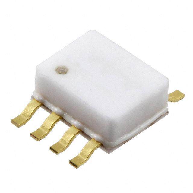
| 产品图片 | |
| P1dB | - |
| 产品型号 | PE42721MLBA-Z |
| RF类型 | CATV |
| rohs | 无铅 / 符合限制有害物质指令(RoHS)规范要求 |
| 产品系列 | UltraCMOS®,HaRP™ |
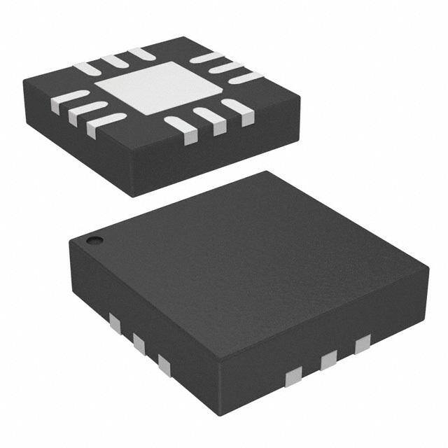
| 供应商器件封装 | 12-QFN(3x3) |
| 其它名称 | 1046-1089-6 |
| 包装 | Digi-Reel® |
| 封装/外壳 | 12-WQFN 裸露焊盘 |
| 工作温度 | -40°C ~ 85°C |
| 拓扑 | 吸收性 |
| 插损@频率 | 0.65dB @ 2.2GHz |
| 标准包装 | 1 |
| 特性 | - |
| 电压-电源 | 2.3 V ~ 5.5 V |
| 电路 | SPDT |
| 阻抗 | 75 欧姆 |
| 隔离@频率 | 55dB @ 2.2GHz (标准) |
| 频率 -上 | 2.2GHz |
| 频率 -下 | 5MHz |


PDF Datasheet 数据手册内容提取
Product Specification PE42721 UltraCMOS® SPDT RF Switch 5–2200 MHz Product Description Features The PE42721 is a HaRP™ technology-enhanced absorptive 75Ω SPDT RF switch developed on the HaRP™ technology enhanced UltraCMOS® process technology. High linearity CTB of -99 dBc PE42721 is a highly linear device delivering high isolation and very low insertion loss performance. It is CSO better than -105 dBc designed for broadband applications such as TV Supports +1.8V control logic tuner modules, CATV signal switching and Low insertion loss distribution, DTV, multi-tuner digital video recorders 0.40 dB @ 220 MHz (DVRs) and set-top boxes. 0.50 dB @ 870 MHz PE42721 supports +1.8V control logic and offers high 0.65 dB @ 2200 MHz ESD protection. PE42721 is pin compatible to High isolation PE42750. In addition, no blocking capacitors are 85 dB @ 220 MHz required if DC voltage is not present on the RF ports. 68 dB @ 870 MHz Peregrine’s HaRP™ technology enhancement is an 53 dB @ 2200 MHz innovative feature of the UltraCMOS® process, ESD performance offering the performance of GaAs with the economy 3kV HBM on RF pins to GND and integration of conventional CMOS. 2kV HBM on all other pins 1kV CDM on all pins Figure 1. Functional Diagram Figure 2. Package Type RFC 12-lead 3x3 mm QFN D S E RF1 RF2 ESD ESD 75 75 CMOS Control Driver and ESD CTRL1 CTRL2 DOC-78344 Document No. DOC-13814-4 │ www.psemi.com ©2013-2016 Peregrine Semiconductor Corp. All rights reserved. Page 1 of 12
PE42721 Product Specification Table 1. Electrical Specifications Temp = +25°C, V = 3.3V (Z = Z = 75Ω) DD S L Parameter Path Condition Min Typ Max Unit Operational frequency 5 2200 MHz 5–220 MHz 0.40 0.55 dB Insertion loss RFC–RFX 221–870 MHz 0.50 0.70 dB 871–2200 MHz 0.65 0.85 dB 5–220 MHz 81 85 dB Isolation RFX–RFX 221–870 MHz 65 68 dB 871–2200 MHz 52 53 dB 5–220 MHz 68 70 dB Isolation RFC–RFX 221–870 MHz 57 59 dB 871–2200 MHz 53 55 dB 870 MHz 18 dB Return loss All ports 2200 MHz 15 dB Input 0.1 dB compression1,2 RFC–RFX 45–1000 MHz 27 dBm IIP23 RFX 45–2200 MHz 110 dBm IIP3 RFX 5–2200 MHz 60 dBm CTB 159 channels; 42 dBmV per channel output power -99 dBc CSO 159 channels; 42 dBmV per channel output power < -105 dBc Cross modulation distortion 159 channels; 42 dBmV per channel output power -89.5 dBc Video feedthrough DC measurement 4 mV PP Switching time 50% CTRL to 90% or 10% RF 1 1.5 μs Notes: 1. The input 0.1 dB compression point (P0.1dB) is a linearity figure of merit. Refer to Table 3 for the RF input power PIN 2. P0.1dB = 25 dBm @ 2.2 GHz 3. IIP2 = 83 dBm @ 5 MHz ©2013-2016 Peregrine Semiconductor Corp. All rights reserved. Document No. DOC-13814-4 │ UltraCMOS® RFIC Solutions Page 2 of 12
PE42721 Product Specification Figure 3. Pin Configuration (Top View) Table 3. Operating Ranges 1 2 RL RL Parameter Symbol Min Typ Max Unit Pin 1 Dot DD T T Marking V C C Supply voltage VDD 2.3 3.3 5.5 V 2 1 0 1 1 1 Supply current IDD 110 200 µA Digital input high GND 1 9 GND (CTRL1, CTRL2) VIH 1.17 3.6 V Exposed RF1 2 Ground 8 RF2 D(CigTiRtaLl 1in, pCuTt RloLw2 ) VIL -0.3 0.6 V Pad GND 3 7 GND Digital input current I 1 µA CTRL RF input power (RFC–RFX)1 4 5 6 5 ≤ 45 MHz P 18 dBm IN D C D 45 ≤ 2200 MHz 22 dBm N F N G R G RF input power into terminated ports (RFX)1 Table 2. Pin Descriptions 5 ≤ 45 MHz P 16 dBm IN,TERM Pin # Pin Name Description 45 ≤ 2200 MHz 16 dBm 1 GND RF Ground Operating temperature range TOP -40 +25 +85 °C 2 RF11 RF Port 1 Note 1: 100% duty cycle, all bands, 75Ω 3 GND RF Ground 4 GND RF Ground Table 4. Absolute Maximum Ratings 5 RFC1 RF Common Parameter/Condition Symbol Min Max Unit 6 GND RF Ground 7 GND RF Ground Supply voltage VDD -0.3 5.5 V 8 RF21 RF Port 2 Digital input voltage VCTRL -0.3 3.6 V 9 GND RF Ground RF input power (RFC–RFX)1 10 CTRL2 Digital control logic input 2 5 ≤ 45 MHz P 18 dBm IN 11 CTRL1 Digital control logic input 1 45 ≤ 2200 MHz 22 dBm 12 V Supply Voltage DD RF input power into terminated Pad GND Exposed pad: Ground for proper operation ports (RFX)1 5 ≤ 45 MHz P 16 dBm IN,TERM Note 1: RF pins 2, 5, and 8 must be at 0V DC. The RF pins do not require DC 45 ≤ 2200 MHz 16 dBm blocking capacitors for proper operation if the 0V DC requirement is met Storage temperature range TST -65 +150 °C ESD voltage HBM2 Exceeding absolute maximum ratings may cause RF pins to GND VESD,HBM 3000 V permanent damage. Operation should be restricted All other pins 2000 V to the limits in the Operating Ranges table. ESD voltage MM3, all pins V 100 V ESD,MM Operation between operating range maximum and ESD Voltage CDM4, all pins V 1000 V ESD,CDM absolute maximum for extended periods may Notes: 1. 100% duty cycle, all bands, 75Ω reduce reliability. 2. Human Body Model (MIL-STD-883 Method 3015) 3. Machine Model (JEDEC JESD22-A115) 4. Charged Device Model (JEDEC JESD22-C101) Document No. DOC-13814-4 │ www.psemi.com ©2013-2016 Peregrine Semiconductor Corp. All rights reserved. Page 3 of 12
PE42721 Product Specification Electrostatic Discharge (ESD) Precautions Table 5. Truth Table1 When handling this UltraCMOS® device, observe C1 C2 RFC – RF1 RFC – RF2 the same precautions that you would use with Low Low ON OFF other ESD-sensitive devices. Although this device Low High OFF ON contains circuitry to protect it from damage due to High Low OFF ON ESD, precautions should be taken to avoid High High ON OFF exceeding the specified rating. Note 1: A versatile logic table has been established to allow either C1 or C2 to act as a single pin control and in either polarity Latch-Up Avoidance Unlike conventional CMOS devices, UltraCMOS® Spurious Performance devices are immune to latch-up. The typical spurious performance of the PE42721 is –124 dBm. Switching Frequency Moisture Sensitivity Level The PE42721 has a maximum 25 kHz switching The Moisture Sensitivity Level rating for the rate. PE42721 in the 12-lead 3x3 mm QFN package is MSL1. Switching frequency describes the time duration between switching events. Switching time is the time duration between the point the control signal reaches 50% of the final value and the point the output signal reaches within 10% or 90% of its target value. Switching time is provided in Table 1. ©2013-2016 Peregrine Semiconductor Corp. All rights reserved. Document No. DOC-13814-4 │ UltraCMOS® RFIC Solutions Page 4 of 12
PE42721 Product Specification Typical Performance Data @ 25°C and V = 3.3V unless otherwise specified DD Figure 4. Insertion Loss (RFC-RFX) Figure 5. Insertion Loss vs. Temp (RFC-RFX) Figure 6. Insertion Loss vs. V (RFC-RFX) DD Document No. DOC-13814-4 │ www.psemi.com ©2013-2016 Peregrine Semiconductor Corp. All rights reserved. Page 5 of 12
PE42721 Product Specification Typical Performance Data @ 25°C and V = 3.3V unless otherwise specified DD Figure 7. RFC Port Return Loss vs. Temp Figure 8. RFC Port Return Loss vs. V DD (RF1 Active) (RF1 Active) Figure 9. RFC Port Return Loss vs. Temp Figure 10. RFC Port Return Loss vs. V DD (RF2 Active) (RF2 Active) ©2013-2016 Peregrine Semiconductor Corp. All rights reserved. Document No. DOC-13814-4 │ UltraCMOS® RFIC Solutions Page 6 of 12
PE42721 Product Specification Typical Performance Data @ 25°C and V = 3.3V unless otherwise specified DD Figure 11. Active Port Return Loss vs. Temp Figure 12. Active Port Return Loss vs. V DD (RF1 Active) (RF1 Active) Figure 13. Active Port Return Loss vs. Temp Figure 14. Active Port Return Loss vs. V DD (RF2 Active) (RF2 Active) Document No. DOC-13814-4 │ www.psemi.com ©2013-2016 Peregrine Semiconductor Corp. All rights reserved. Page 7 of 12
PE42721 Product Specification Typical Performance Data @ 25°C and V = 3.3V unless otherwise specified DD Figure 15. Isolation vs. Temp (RFX-RFX) Figure 16. Isolation vs. V (RFX-RFX) DD Figure 17. Isolation vs. Temp (RFC-RFX) Figure 18. Isolation vs. V (RFC-RFX) DD ©2013-2016 Peregrine Semiconductor Corp. All rights reserved. Document No. DOC-13814-4 │ UltraCMOS® RFIC Solutions Page 8 of 12
PE42721 Product Specification Evaluation Board Figure 19. Evaluation Board Layout The SPDT switch evaluation board was designed to ease customer evaluation of Peregrine’s PE42721. The RF common port is connected through a 75Ω transmission line via the F-Type connector, J2. RF1 and RF2 ports are connected through 75Ω transmission lines via F-Type connectors J1 and J3, respectively. A 75Ω through transmission line is available via F-Type connectors J4 and J5, which can be used to de-embed the loss of the PCB. J6 provides DC and digital inputs to the device. PRT-51234 Document No. DOC-13814-4 │ www.psemi.com ©2013-2016 Peregrine Semiconductor Corp. All rights reserved. Page 9 of 12
PE42721 Product Specification Figure 20. Evaluation Board Schematic DOC-02571 ©2013-2016 Peregrine Semiconductor Corp. All rights reserved. Document No. DOC-13814-4 │ UltraCMOS® RFIC Solutions Page 10 of 12
PE42721 Product Specification Figure 21. Package Drawing 12-lead 3x3 mm QFN DOC-53275 Figure 22. Top Marking Specifications 42721 = Pin 1 designator YYWW YY = Last two digits of assembly year ZZZZZZ WW = Assembly work week ZZZZZZ = Assembly lot code (maximum six characters) DOC-64916 Document No. DOC-13814-4 │ www.psemi.com ©2013-2016 Peregrine Semiconductor Corp. All rights reserved. Page 11 of 12
PE42721 Product Specification Figure 23. Tape and Reel Drawing Tape Feed Direction Ao = 3.30 ± 0.1 mm Pin 1 Bo = 3.30 ± 0.1 mm Ko = 1.10 ± 0.1 mm Top of Device Device Orientation in Tape Table 6. Ordering Information Order Code Description Package Shipping Method PE42721MLBA-Z PE42721 SPDT RF switch Green 12-lead 3x3 mm QFN 3000 units/T&R EK42721-02 PE42721 Evaluation kit Evaluation kit 1/Box Sales Contact and Information For sales and contact information please visit www.psemi.com. Advance Information: The product is in a formative or design stage. The datasheet contains design target No patent rights or licenses to any circuits described in this datasheet are implied or granted to any third party. specifications for product development. Specifications and features may change in any manner without notice. Peregrine’s products are not designed or intended for use in devices or systems intended for surgical implant, Preliminary Specification: The datasheet contains preliminary data. Additional data may be added at a later or in other applications intended to support or sustain life, or in any application in which the failure of the date. Peregrine reserves the right to change specifications at any time without notice in order to supply the best Peregrine product could create a situation in which personal injury or death might occur. Peregrine assumes no possible product. Product Specification: The datasheet contains final data. In the event Peregrine decides to liability for damages, including consequential or incidental damages, arising out of the use of its products in change the specifications, Peregrine will notify customers of the intended changes by issuing a CNF (Customer such applications. Notification Form). The Peregrine name, logo, UltraCMOS and UTSi are registered trademarks and HaRP, MultiSwitch and DuNE The information in this datasheet is believed to be reliable. However, Peregrine assumes no liability for the use are trademarks of Peregrine Semiconductor Corp. Peregrin e products are protected under one or more of of this information. Use shall be entirely at the user’s own risk. the following U.S. Patents: http://patents.psemi.com. ©2013-2016 Peregrine Semiconductor Corp. All rights reserved. Document No. DOC-13814-4 │ UltraCMOS® RFIC Solutions Page 12 of 12