ICGOO在线商城 > 射频/IF 和 RFID > RF 开关 > UPG2406TK-E2-A
 Datasheet下载
- 型号: UPG2406TK-E2-A
- 制造商: CEL
- 库位|库存: xxxx|xxxx
- 要求:
| 数量阶梯 | 香港交货 | 国内含税 |
| +xxxx | $xxxx | ¥xxxx |
查看当月历史价格
查看今年历史价格
UPG2406TK-E2-A产品简介:
ICGOO电子元器件商城为您提供UPG2406TK-E2-A由CEL设计生产,在icgoo商城现货销售,并且可以通过原厂、代理商等渠道进行代购。 UPG2406TK-E2-A价格参考。CELUPG2406TK-E2-A封装/规格:RF 开关, 射频开关 IC 蓝牙,WLAN SPDT 3GHz 50 欧姆 6-迷你型模塑。您可以下载UPG2406TK-E2-A参考资料、Datasheet数据手册功能说明书,资料中有UPG2406TK-E2-A 详细功能的应用电路图电压和使用方法及教程。
CEL品牌的UPG2406TK-E2-A是一款RF(射频)开关,广泛应用于通信和射频系统中。该器件为GaAs MMIC(单片微波集成电路)制成,具备低插入损耗、高隔离度和快速切换速度等特性,适用于需要高频信号控制的场景。

其主要应用场景包括:

1. 无线通信设备:用于基站、无线接入点和通信模块中,实现射频信号路径的切换,如收发切换或天线切换。

2. 测试与测量仪器:在射频测试系统中,作为信号路径控制元件,用于自动测试设备(ATE)或频谱分析仪中。

3. 工业控制系统:用于远程监控和控制系统中的射频信号管理,如工业物联网(IIoT)设备。

4. 雷达与安防系统:在雷达接收/发射切换、安防监控设备中实现信号路由控制。

5. 消费类电子产品:如高端路由器、智能天线系统等需要射频信号切换的场合。

该器件采用小型TSSOP封装,适合高密度PCB布局,工作温度范围宽,适用于工业级环境。
| 参数 | 数值 |
| 产品目录 | |
| 描述 | IC SPDT 10MHZ-3GHZ 6-MINIMOLD |
| 产品分类 | |
| IIP3 | 60dBm (标准) |
| 品牌 | CEL |
| 数据手册 | |
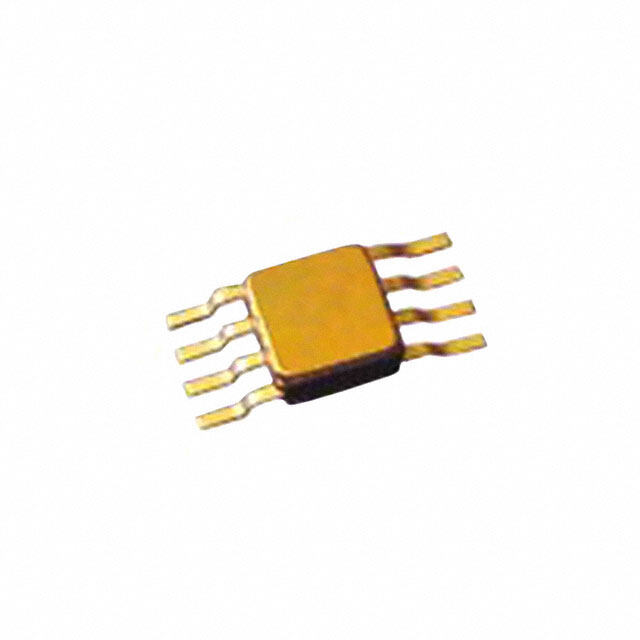
| 产品图片 |
|
| P1dB | 30.5dBm (标准) IP1dB |
| 产品型号 | UPG2406TK-E2-A |
| RF类型 | Bluetooth,WLAN |
| rohs | 无铅 / 符合限制有害物质指令(RoHS)规范要求 |
| 产品系列 | - |
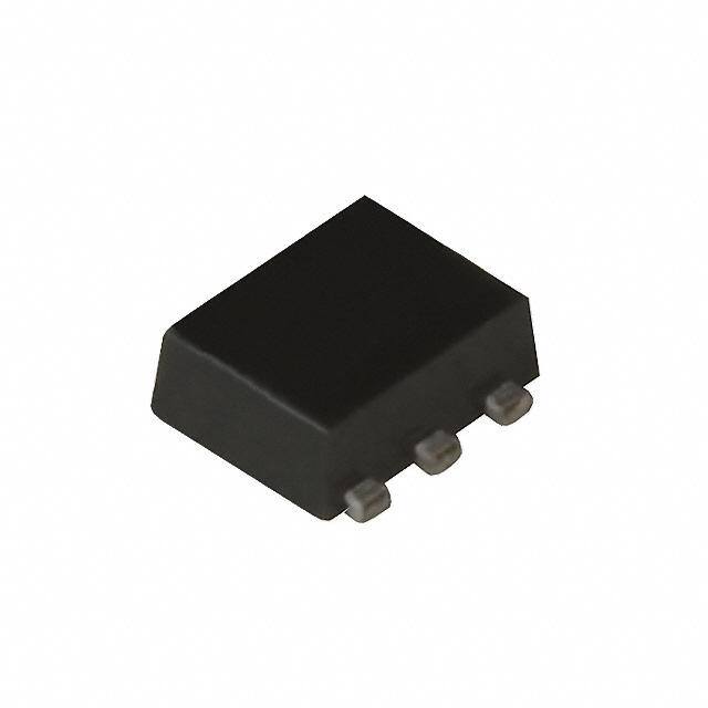
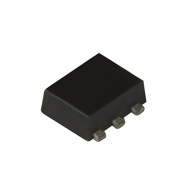
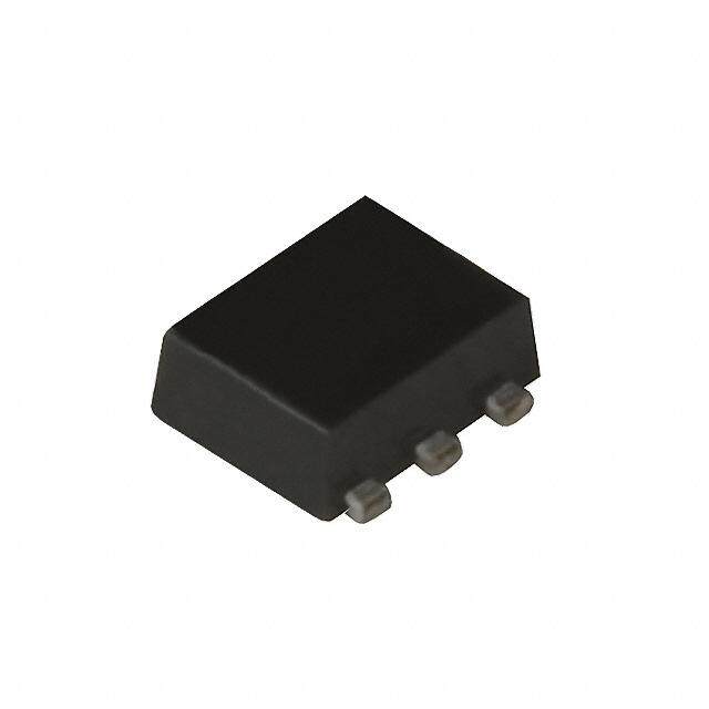
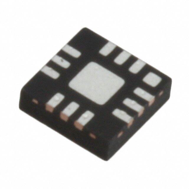
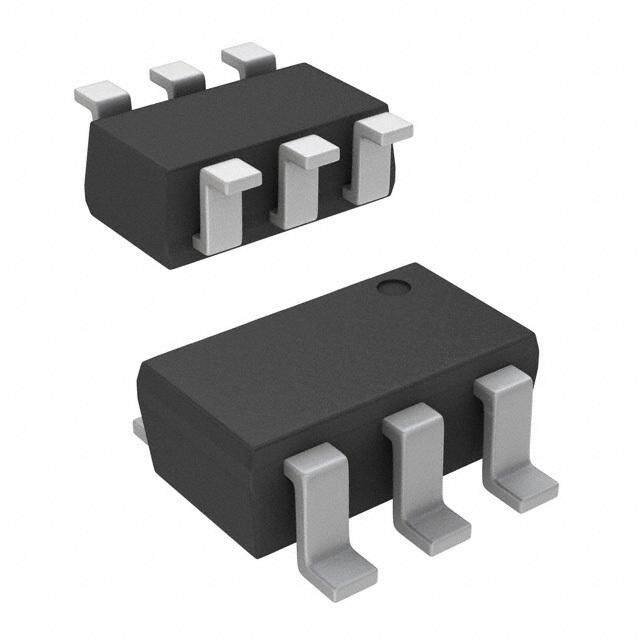
| 供应商器件封装 | 6-迷你型模塑 |
| 其它名称 | UPG2406TK-E2-ADKR |
| 包装 | Digi-Reel® |
| 封装/外壳 | 6-SMD,扁平引线 |
| 工作温度 | -45°C ~ 85°C |
| 拓扑 | 反射 |
| 插损@频率 | 0.53dB @ 3GHz |
| 标准包装 | 1 |
| 特性 | - |
| 电压-电源 | - |
| 电路 | SPDT |
| 阻抗 | 50 欧姆 |
| 隔离@频率 | 17dB @ 3GHz (标准) |
| 频率 -上 | 3GHz |
| 频率 -下 | 10MHz |


- 商务部:美国ITC正式对集成电路等产品启动337调查
- 曝三星4nm工艺存在良率问题 高通将骁龙8 Gen1或转产台积电
- 太阳诱电将投资9.5亿元在常州建新厂生产MLCC 预计2023年完工
- 英特尔发布欧洲新工厂建设计划 深化IDM 2.0 战略
- 台积电先进制程称霸业界 有大客户加持明年业绩稳了
- 达到5530亿美元!SIA预计今年全球半导体销售额将创下新高
- 英特尔拟将自动驾驶子公司Mobileye上市 估值或超500亿美元
- 三星加码芯片和SET,合并消费电子和移动部门,撤换高东真等 CEO
- 三星电子宣布重大人事变动 还合并消费电子和移动部门
- 海关总署:前11个月进口集成电路产品价值2.52万亿元 增长14.8%


PDF Datasheet 数据手册内容提取
GaAs INTEGRATED CIRCUIT PG2406TK D 6 0.01 to 3.0 GHz SPDT SWITCH E M 6 DESCRIPTION U The PG2406TK is a GaAs MMIC for L, S-band SPDT (Single Pole Double Throw) switch 0which were designed for mobile phone and another L, S-band application. 4 This device can operate 2 control switching by control voltage 1.8 to 5.3 V. This device can operate frequency N from 0.01 to 3.0 GHz, having the low insertion loss and high isolation. 2 This device is housed in a 6-pin lead-less minimold package. And this package is able to high-density surface mounting. G FEATURES I C • Switch control voltage : Vcont (H) = 1.8 to 5T.3 V (2.7 V TYP.) : Vcont (L) = 0.2 to +0.2 V (0 V TYP.) : • Low insertion loss : Lins = 0.40 dB TYP. @ f = 1.0 GHzt, Vcont (H) = 2.7 V, Vcont (L) = 0 V : Lins = 0.47 dB TYP. @ f = 2.5 GHnz, Vcont (H) = 2.7 V, Vcont (L) = 0 V N • High isolation : ISL = 27 dB TYP. @ f = 1.0 GHz, Vcont (H) = 2.7 V, Vcont (L) = 0 V : ISL = 17 dB TYP. @ f = 2.5 eGHz, Vcont (H) = 2.7 V, Vcont (L) = 0 V • Handling power : Pin (0.1 dB) = +29.0 dBm TYmP. @ f = 2.0/2.5 GHz, Vcont (H) = 2.7 V, Vcont (L) = 0 V : Pin (1 dB) = +30.5 dBm TYP. @ f = 0.5 to 3.0 GHz, Vcont (H) = 2.7 V, Vcont (L) = 0 V O • High-density surface mounting : 6-pin lead-less minimold package (1.5 1.1 0.55 mm) e APPLICATIONS c • L, S-band digital cellular or cordless telephone a • W-LAN, WLL and BlCuetoothTM etc. l ORDERING INFORMATION p e Part Number Order Number Package Marking Supplying Form S PG2406TK-E2 PG2406TK-E2-A R6-pin lead-less minimold G5K Embossed tape 8 mm wide (1511 PKG) (Pb-Free) Pin 1, 6 face the perforation side of the tape Qty 5 kpcs/reel n I Remark To order evaIluation samples, contact your nearby sales office. D Part numb-er for sample order: PG2406TK-A p o r CDaution Although this device is designed to be as robust as possible, ESD (Electrostatic Discharge) can damage this device. This device must be protected at all times from ESD. Static charges may easily produce potentials of several kilovolts on the human body or equipment, which can discharge without detection. Industry-standard ESD precautions must be employed at all times. Document No. PG10746EJ01V0DS (1st edition) Date Published January 2009 NS
PG2406TK PIN CONNECTIONS AND INTERNAL BLOCK DIAGRAM D Pin No. Pin Name 6 1 RF1 E 2 GMND 3 RF2 4 6Vcont2 U 5 RFC 0 6 Vcont1 4 SW TRUTH TABLE N 2 ON Path Vcont1 Vcont2 G RFC-RF1 High Low RFC-RF2 Low High I C T ABSOLUTE MAXIMUM RATINGS (TA = +25C, unless otherwise specified) : t Parameter Symbol Ratings Unit n N Switch Control Voltage Vcont +6.0 Note V e Input Power f = 0.01 to 0.5 GHz Pin1 +24.0 dBm m f = 0.5 to 3.0 GHz Pin2 +31.0 O Operating Ambient Temperature TA 45 to +85 C e Storage Temperature Tstg 55 to +150 C c Note Vcont1 Vcont2 6.0 V a C RECOMMENDED OPERATING RANGlE (TA = +25C, unless otherwise specified) p Parameter Symbol MIN. TYP. MAX. Unit e Switch ControlS Voltage (H) Vcont (H) 1.8 2.7 5.3 V R Switch Control Voltage (L) Vcont (L) 0.2 0 0.2 V n I I D - p o r D 2 Data Sheet PG10746EJ01V0DS
PG2406TK ELECTRICAL CHARACTERISTICS D (TA = +25C, Vcont (H) = 2.7 V, Vcont (L) = 0 V, DC blocking capacitors = 56 pF, unless otherwise specified) 6 Parameter Symbol Test Conditions MINE. TYP. MAX. Unit Insertion Loss 1 Lins1 f = 0.01 to 0.05 GHz Note 1 0.40 M dB Insertion Loss 2 Lins2 f = 0.05 to 0.5 GHz Note 2 0.40 0.45 dB 6 Insertion Loss 3 Lins3 f = 0.5 to 1.0 GHz U 0.40 0.45 dB Insertion Loss 4 Lins4 f = 1.0 to 2.0 GHz 0.450 0.50 dB Insertion Loss 5 Lins5 f = 2.0 to 2.5 GHz 0.47 0.55 dB 4 Insertion Loss 6 Lins6 f = 2.5 to 3.0 GHz 0.53 0.60 dB N Isolation 1 ISL1 f = 0.01 to 0.05 GHz Note 1 227 dB Isolation 2 ISL2 f = 0.05 to 0.5 GHz Note 2 23 27 dB G Isolation 3 ISL3 f = 0.5 to 1.0 GHz 23 27 dB Isolation 4 ISL4 f = 1.0 to 2.0I GHz C16 19 dB Isolation 5 ISL5 f = 2.0 toT 2.5 GHz 14 17 dB Isolation 6 ISL6 f = 2.5 to 3.0 GHz 14 17 dB : Input Return Loss 1 RLin1 f = 0.01 to 0.05 GHz Note 1 t 20 dB n Input Return Loss 2 RLin2 Nf = 0.05 to 0.5 GHz Note 2 15 20 dB Input Return Loss 3 RLin3 f = 0.5 to 3.0 GHz e 15 20 dB Output Return Loss 1 RLout1 f = 0.01 to 0.05 GmHz Note 1 20 dB Output Return Loss 2 ORLout2 f = 0.05 to 0.5 GHz Note 2 15 20 dB Output Return Loss 3 RLout3 f = 0.5 to 3e.0 GHz 15 20 dB 0.1 dB Loss Compression Pin (0.1 dB) f = 2.0c/2.5 GHz +26.0 +29.0 dBm Input Power Note 3 f = 0.5 to 3.0 GHz +29.0 dBm a C 1 dB Loss Compression Pin (1 dB) f = 0.5 to 3.0 GHz +30.5 dBm l Input Power Note 4 p 2nd Harmonics 2f0 f = 2.0/2.5 GHz, Pin = +20 dBm 65 75 dBc e 3rd HarmonicsS 3f0 f = 2.0/2.5 GHz, Pin = +20 dBm 65 75 dBc R Intermodulation Intercept Point IIP3 f = 0.5 to 3.0 GHz, 2 tone, +60 dBm 5 MHz spicing Switch Control Current n Icont No RF input 0.2 20 A I Switch Control Speed I tSW 50% CTL to 90/10% RF 50 500 ns D - Notes 1. DC blockping capacitors = 10 000 pF at f = 0.01 to 0.05 GHz 2. DC blocking capacitors = 1 000 pF at f = 0.05 to 0.5 GHz 3. Pin (0o.1 dB) is measured the input power level when the insertion loss increases more 0.1 dB than that of linear range. r 4. Pin (1 dB) is measured the input power level when the insertion loss increases more 1 dB than that of D linear range. Caution This device is used it is necessary to use DC blocking capacitors. The value of DC blocking capacitors should be chosen to accommodate the frequency of operation, bandwidth, switching speed and the condition with actual board of your system. The range of recommended DC blocking capacitor value is less than 56 pF. 3 Data Sheet PG10746EJ01V0DS
PG2406TK ELECTRICAL CHARACTERISTICS D (TA = +25C, Vcont (H) = 1.8 V, Vcont (L) = 0 V, DC blocking capacitors = 56 pF, unless otherwise specified) 6 Parameter Symbol Test Conditions MINE. TYP. MAX. Unit Insertion Loss 7 Lins7 f = 0.01 to 0.05 GHz Note 1 0.40 M dB Insertion Loss 8 Lins8 f = 0.05 to 0.5 GHz Note 2 0.40 0.46 dB 6 Insertion Loss 9 Lins9 f = 0.5 to 1.0 GHz U 0.40 0.47 dB Insertion Loss 10 Lins10 f = 1.0 to 2.0 GHz 0.460 0.52 dB Insertion Loss 11 Lins11 f = 2.0 to 2.5 GHz 0.48 0.57 dB 4 Insertion Loss 12 Lins12 f = 2.5 to 3.0 GHz 0.54 0.62 dB N Isolation 7 ISL7 f = 0.01 to 0.05 GHz Note 1 227 dB Isolation 8 ISL8 f = 0.05 to 0.5 GHz Note 2 23 27 dB G Isolation 9 ISL9 f = 0.5 to 1.0 GHz 23 27 dB Isolation 10 ISL10 f = 1.0 to 2.0I GHz C16 19 dB Isolation 11 ISL11 f = 2.0 toT 2.5 GHz 14 17 dB Isolation 12 ISL12 f = 2.5 to 3.0 GHz 14 17 dB : Input Return Loss 4 RLin4 f = 0.01 to 0.05 GHz Note 1 t 20 dB n Input Return Loss 5 RLin5 Nf = 0.05 to 0.5 GHz Note 2 15 20 dB Input Return Loss 6 RLin6 f = 0.5 to 3.0 GHz e 15 20 dB Output Return Loss 4 RLout4 f = 0.01 to 0.05 GmHz Note 1 20 dB Output Return Loss 5 ORLout5 f = 0.05 to 0.5 GHz Note 2 15 20 dB Output Return Loss 6 RLout6 f = 0.5 to 3e.0 GHz 15 20 dB 0.1 dB Loss Compression Pin (0.1 dB) f = 2.0c/2.5 GHz +19.0 +22.0 dBm Input Power Note 3 f = 0.5 to 3.0 GHz +22.0 dBm a C 1 dB Loss Compression Pin (1 dB) f = 0.5 to 3.0 GHz +25.0 dBm l Input Power Note 4 p Switch Control Current Icont No RF input 0.2 20 A e Switch ControlS Speed tSW 50% CTL to 90/10% RF 50 500 ns R Notes 1. DC blocking capacitors = 10 000 pF at f = 0.01 to 0.05 GHz 2. DC blocking capnacitors = 1 000 pF at f = 0.05 to 0.5 GHz I 3. Pin (0.1 dB) is measured the input power level when the insertion loss increases more 0.1 dB than that of I D linear rang-e. 4. Pin (1 dB) ips measured the input power level when the insertion loss increases more 1 dB than that of linear range. o Caution This device is used it is necessary to use DC blocking capacitors. r The value of DC blocking capacitors should be chosen to accommodate the frequency of D operation, bandwidth, switching speed and the condition with actual board of your system. The range of recommended DC blocking capacitor value is less than 56 pF. 4 Data Sheet PG10746EJ01V0DS
PG2406TK EVALUATION CIRCUIT D 6 E M 6 U 0 4 N 2 G Note C1 : 0.01 to 0.05 GHz 10 000 pF : 0.05 to 0.5 GHz 1 000 pF I C : 0.5 to 3.0 GHz 56 pF T C2 : 1 000 pF The application circuits and their parameters are for reference only a:nd are not intended for use in actual design-ins. t N n APPLICATION INFORMATION e m O e c a C • LESD provides a means to increase the ESD protection on a specific RF port, typically the port attached to the l antenna. p • The value may be tailored to provide specific electrical responses. • The RF ground connections shoueld be kept as short as possible and connected to directly to a good RF ground S for best performance. R n I I D - p o r D 5 Data Sheet PG10746EJ01V0DS
PG2406TK ILLUSTRATION OF THE TEST CIRCUIT ASSEMBLED ON EVALUATION BOADRD 6 E M 6 U 0 4 N 2 G I C T : t n N e m O e c a C l p e USING THE EVALUATION BOARD S R Symbol Test Conditions Values C1 f = 0.01 to 0.05 GH z 10 000 pF n If = 0.05 to 0.5 GHz 1 000 pF I D f = 0.5 to 3-.0 GHz 56 pF C2 p 1 000 pF o r D 6 Data Sheet PG10746EJ01V0DS
PG2406TK TYPICAL CHARACTERISTICS (TA = +25C, DC blocking capacitors = 56 pF, unless othDerwise specified) 6 E M 6 U 0 4 N 2 G I C T : t n N e m O e c a C l p e S R n I I D - p o r D Remark The graphs indicate nominal characteristics. 7 Data Sheet PG10746EJ01V0DS
PG2406TK D 6 E M 6 U 0 4 N 2 G I C T : t n N e m O e c a C l p e S R n I I D - p o r D Remark The graphs indicate nominal characteristics. 8 Data Sheet PG10746EJ01V0DS
PG2406TK MOUNTING PAD LAYOUT DIMENSIONS D 6-PIN LEAD-LESS MINIMOLD (1511 PKG) (UNIT: mm) 6 E M 6 U 0 4 N 2 G I C Remark The mounting pad layout in this document is for reference only. T : t n N e m O e c a C l p e S R n I I D - p o r D 9 Data Sheet PG10746EJ01V0DS
PG2406TK PACKAGE DIMENSIONS D 6-PIN LEAD-LESS MINIMOLD (1511 PKG) (UNIT: mm) 6 E M 6 U 0 4 N 2 G I C T : t n N e m O e c a C l p e S R n I I D - p o r D 10 Data Sheet PG10746EJ01V0DS
PG2406TK RECOMMENDED SOLDERING CONDITIONS D This product should be soldered and mounted under the following recommended conditions. For soldering methods and conditions other than those recommended below, contact your nearby sales office. 6 Soldering Method Soldering Conditions E Condition Symbol M Infrared Reflow Peak temperature (package surface temperature) : 260C or below IR260 Time at peak temperature : 10 seconds or less Time at temperature of 220C or higher : 60 seconds or less 6 Preheating time at 120 to 180C :U 12030 seconds Maximum number of reflow processes : 3 times 0 Maximum chlorine content of rosin flux (% mass) : 0.2%(Wt.) or below Wave Soldering Peak temperature (molten solder temperature) : 260C or below 4 WS260 Time at peak temperature N: 10 seconds or less Preheating temperature (package surface temperature) : 120C or belo2w Maximum number of flow processes : 1 time G Maximum chlorine content of rosin flux (% mass) : 0.2%(Wt.) or below Partial Heating Peak temperature (terminal temperature) : 350C or below HS350 I C Soldering time (per side of device) : 3 seconds or less Maximum chlorine content of rosTin flux (% mass) : 0.2%(Wt.) or below : Caution Do not use different soldering methods together (except for partial heating). t n N e m O e c a C l p e S R n I I D - p o r D 11 Data Sheet PG10746EJ01V0DS
PG2406TK This product uses gallium arsenide (GaAs). D Caution GaAs Products GaAs vapor and powder are hazardous to human health if inhaled or ingested, so please observe the following points. • Follow related laws and ordinances when disposing of the product. If there are no applicable laws 6 and/or ordinances, dispose of the product as recommended below. E 1. Commission a disposal company able to (with a license to) collect, transport and dispose of M materials that contain arsenic and other such industrial waste materials. 2. Exclude the product from general industrial waste and household garbage, and ensure that the product is controlled (as industrial waste subject to special control) up until final d6isposal. U • Do not burn, destroy, cut, crush, or chemically dissolve the product. 0 • Do not lick the product or in any way allow it to enter the mouth. 4 N 2 G I C T : t n N e m O e c a C l p e S R n I I D - p o r D 12 Data Sheet PG10746EJ01V0DS
NOTICE D 1. Descriptions of circuits, software and other related information in this document are provided only to illustrate the operation of semiconductor products and application examples. You are fully responsible for the incorporation of these circuits, software, and information in the design of your equipment. California Eastern Laboratories and Renesas Electronics assumes no responsibility for any losses incurred by you or third parties arising from the use of 6these circuits, software, or information. E 2. California Eastern Laboratories has used reasonable care in preparing the information included in this document, but California Eastern Laboratories does M not warrant that such information is error free. California Eastern Laboratories and Renesas Electronics assumes no liability whatsoever for any damages incurred by you resulting from errors in or omissions from the information included herein. 3. California Eastern Laboratories and Renesas Electronics do not assume any liability for infringement of patents, copyrights, or other intellectual property rights of third parties by or arising from the use of Renesas Electronics products or technical information described in this docum6ent. No license, express, implied or otherwise, is granted hereby under any patents, copyrights or other intellectual propertyU rights of California Eastern Laboratories or Renesas Electronics or others. 0 4. You should not alter, modify, copy, or otherwise misappropriate any Renesas Electronics product, whether in whole or in part. California Eastern Laboratories and Renesas Electronics assume no responsibility for any losses incurred by you or third parties arising from such alteration, modification, copy or otherwise misappropriation of Renesas Electronics product. 4 5. Renesas Electronics products are classified according to the following two quality grades: “Standard” and “High Quality”. The recommended applications N for each Renesas Electronics product depends on the product’s quality grade, as indicated below. “Standard”: Computers; office equipment; communications 2 equipment; test and measurement equipment; audio and visual equipment; home electronic appliances; machine tools; personal electronic equipment; and industrial robots etc. “High Quality”: Transportation equipment (automobiles, trains, ships, etc.); traffic control systems; anti-disaster systems; anti-crime systems; and safety equipment etc. Renesas Electronics products are neither intended nor authorized for useG in products or systems that may pose a direct threat to human life or bodily injury (artificial life support devices or systems, surgical implantations etc.), or may cause serious property damages (nuclear reactor control systems, military equipment etc.). You must check the quality grade of each Renesas Electronics product before using it in a particular application. You may not use any Renesas Electronics product for any apIplication for which it is not inCtended. California Eastern Laboratories and Renesas Electronics shall not be in any way liable for any damages or losses incurred by you or thir d parties arising from the use of any Renesas Electronics product for which the product is not intended by California Eastern LaboratoTries or Renesas Electronics. 6. You should use the Renesas Electronics products described in this document within the range specified by California Eastern Laboratories, especially with respect to the maximum rating, operating supply voltage range, movement power voltage ran:ge, heat radiation characteristics, installation and other product characteristics. California Eastern Laboratories shall have no liability for malfunctions or dtamages arising out of the use of Renesas Electronics products beyond such specified ranges. n N 7. Although Renesas Electronics endeavors to improve the quality and reliability of its products, semiconductor products have specific characteristics such as the occurrence of failure at a certain rate and malfunctions under certain use conditions. Further, Renesas Electronics products are not subject to radiation e resistance design. Please be sure to implement safety measures to guard them against the possibility of physical injury, and injury or damage caused by fire in the event of the failure of a Renesas Electronics product, such as safety design for hardware and software including but not limited to redundancy, m fire control and malfunction prevention, appropriate treatment for aging degradation or any other appropriate measures. Because the evaluation of microcomputer software alone is very difficult, please evaluate the safety of the final products or systems manufactured by you. O 8. Please contact a California Eastern Laboratories sales office for details as to environmental matters such as the environmental compatibility of each Renesas Electronics product. Please use Renesas Electronics products in compleiance with all applicable laws and regulations that regulate the inclusion or use of controlled substances, including without limitation, the EU RoHS Directive. California Eastern Laboratories and Renesas Electronics assume no liability for damages or losses occurring as a result of your noncompliance wicth applicable laws and regulations. 9. Renesas Electronics products and technology may not be used for or incorporated into any products or systems whose manufacture, use, or sale is prohibited under any applicable domestic or foreign laws or regulations. aYou should not use Renesas Electronics products or technology described in this document C for any purpose relating to military applications or use by the military, including but not limited to the development of weapons of mass destruction. When exporting the Renesas Electronics products or technologyl described in this document, you should comply with the applicable export control laws and regulations and follow the procedures required by suchp laws and regulations. 10. It is the responsibility of the buyer or distributor of California Eastern Laboratories, who distributes, disposes of, or otherwise places the Renesas Electronics product with a third party, to notify such third party in advance of the contents and conditions set forth in this document, California Eastern Laboratories and e Renesas Electronics assume no responsibility for any losses incurred by you or third parties as a result of unauthorized use of Renesas Electronics products. S 11. This document may not be reproduced or duplicated in any form, in whole or in part, without prior written consent of California Eastern Laboratories. 12. Please contact a California Eastern LaboratorRies sales office if you have any questions regarding the information contained in this document or Renesas Electronics products, or if you have any other inquiries. NOTE 1: “Renesas Electronics” as used in nthis document means Renesas Electronics Corporation and also includes its majority-owned subsidiaries. NOTE 2: “RIenesas Electronics product(s)” means any product developed or manufactured by or for Renesas Electronics. NOTE 3: Products and product informIation are subject to change without notice. D - p CEL Headquarters • 4590 Patrick Henry Drive, Santa Clara, CA 95054 • Phone (408) 919-2500 • www.cel.com o For a complete list of sales offices, representatives and distributors, r Please visit our website: www.cel.com/contactus D