ICGOO在线商城 > 射频/IF 和 RFID > RF 开关 > UPG2214TB-E4-A
 Datasheet下载
- 型号: UPG2214TB-E4-A
- 制造商: CEL
- 库位|库存: xxxx|xxxx
- 要求:
| 数量阶梯 | 香港交货 | 国内含税 |
| +xxxx | $xxxx | ¥xxxx |
查看当月历史价格
查看今年历史价格
UPG2214TB-E4-A产品简介:
ICGOO电子元器件商城为您提供UPG2214TB-E4-A由CEL设计生产,在icgoo商城现货销售,并且可以通过原厂、代理商等渠道进行代购。 UPG2214TB-E4-A价格参考。CELUPG2214TB-E4-A封装/规格:RF 开关, RF Switch IC 802.11a/b/g/WiFi, 802.16/WiMax, WLAN SPDT 3GHz 50Ohm 6-SuperMiniMold。您可以下载UPG2214TB-E4-A参考资料、Datasheet数据手册功能说明书,资料中有UPG2214TB-E4-A 详细功能的应用电路图电压和使用方法及教程。
CEL的UPG2214TB-E4-A是一款RF(射频)开关,属于半导体射频前端器件,广泛应用于需要高频信号切换的电子系统中。该器件适用于工作频率范围较宽的无线通信设备,典型应用场景包括移动通信设备、智能手机、平板电脑、无线局域网(Wi-Fi)、蓝牙模块和物联网(IoT)终端等。

UPG2214TB-E4-A采用小型化封装,适合高密度集成设计,具备低插入损耗和高隔离度特性,能够有效提升射频信号传输质量。它常用于天线切换、多频段射频路径选择以及收发通道切换等场景,例如在手机中实现蜂窝网络(如LTE、5G)与Wi-Fi/蓝牙之间的信号通路切换,确保不同通信模式间互不干扰。

此外,该RF开关还适用于便携式设备,因其低功耗和高可靠性,有助于延长电池续航时间。其稳定的性能也使其可用于工业无线通信模块、车载信息娱乐系统及智能家居设备中的无线连接方案。

总之,UPG2214TB-E4-A凭借其优异的射频性能和紧凑设计,是现代无线通信系统中实现高效信号路由管理的关键元件之一。
| 参数 | 数值 |
| 产品目录 | |
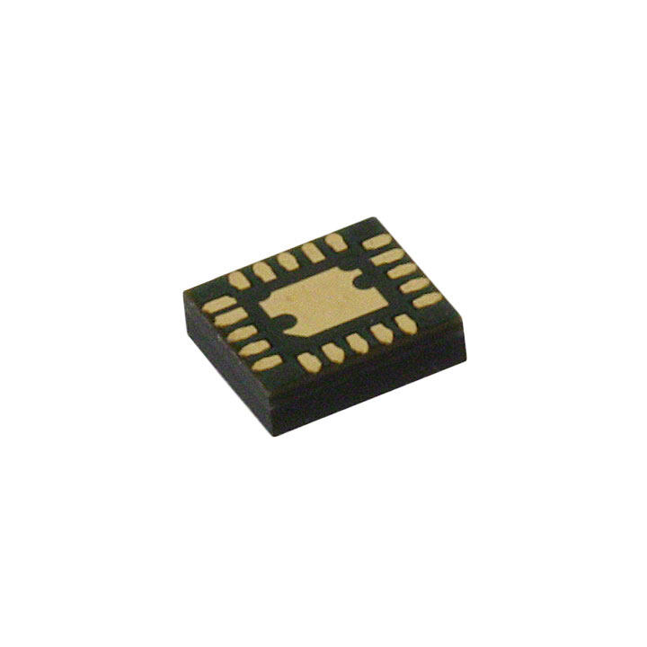
| 描述 | IC SWITCH SPDT 6-SMINIRF 开关 IC 3.0V L S Band SPDT |
| 产品分类 | |
| IIP3 | 58dBm (标准) |
| 品牌 | CEL |
| 产品手册 | |
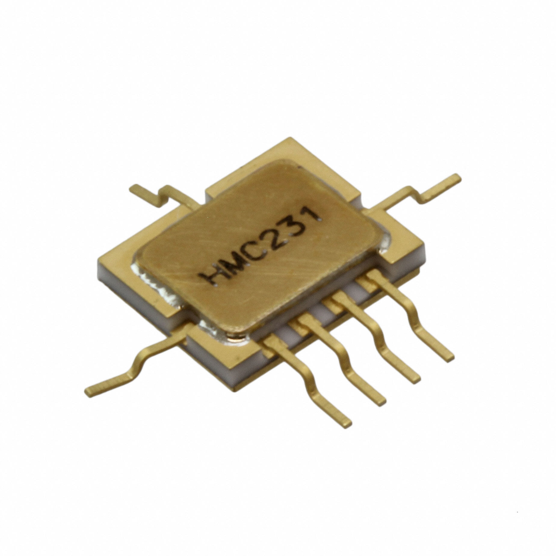
| 产品图片 |
|
| rohs | 符合RoHS无铅 / 符合限制有害物质指令(RoHS)规范要求 |
| 产品系列 | RF集成电路,RF 开关 IC,CEL UPG2214TB-E4-A- |
| 数据手册 | |
| P1dB | 27dBm (标准) IP1dB |
| 产品型号 | UPG2214TB-E4-A |
| RF类型 | 802.11a/b/g/WiFi, 802.16/WiMax, WLAN |
| 产品种类 | RF 开关 IC |
| 介入损耗 | 0.45 dB |
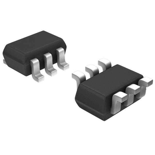
| 供应商器件封装 | 6-SuperMiniMold |
| 关闭隔离—典型值 | 32 dB |
| 其它名称 | UPG2214TB-E4-ACT |
| 包装 | 剪切带 (CT) |
| 商标 | CEL |
| 安装风格 | SMD/SMT |
| 封装 | Reel |
| 封装/外壳 | 6-TSSOP,SC-88,SOT-363 |
| 封装/箱体 | S06 |
| 工作温度 | -45°C ~ 85°C |
| 工厂包装数量 | 3000 |
| 带宽 | 50 MHz to 3000 MHz |
| 开关数量 | Single |
| 开关配置 | SPDT |
| 拓扑 | 反射 |
| 插损@频率 | 0.35dB @ 3GHz |
| 最大工作温度 | + 85 C |
| 最小工作温度 | - 45 C |
| 标准包装 | 1 |
| 特性 | - |
| 电压-电源 | - |
| 电源电压-最大 | 5.3 V |
| 电源电压-最小 | 1.8 V |
| 电路 | SPDT |
| 阻抗 | 50 欧姆 |
| 隔离@频率 | 24dB @ 3GHz (标准) |
| 频率 | 0.05 GHz to 3 GHz |
| 频率 -上 | 3GHz |
| 频率 -下 | 50MHz |
| 高控制电压 | 5.3 V |


- 商务部:美国ITC正式对集成电路等产品启动337调查
- 曝三星4nm工艺存在良率问题 高通将骁龙8 Gen1或转产台积电
- 太阳诱电将投资9.5亿元在常州建新厂生产MLCC 预计2023年完工
- 英特尔发布欧洲新工厂建设计划 深化IDM 2.0 战略
- 台积电先进制程称霸业界 有大客户加持明年业绩稳了
- 达到5530亿美元!SIA预计今年全球半导体销售额将创下新高
- 英特尔拟将自动驾驶子公司Mobileye上市 估值或超500亿美元
- 三星加码芯片和SET,合并消费电子和移动部门,撤换高东真等 CEO
- 三星电子宣布重大人事变动 还合并消费电子和移动部门
- 海关总署:前11个月进口集成电路产品价值2.52万亿元 增长14.8%


PDF Datasheet 数据手册内容提取
A Business Partner of Renesas Electronics Corporation. Preliminary μ Data Sheet PG2214TB R09DS0050EJ0400 Rev.4.00 GaAs Integrated Circuit for L, S-Band SPDT Switch Sep 10, 2012 2 T DESCRIPTION M The μPG2214TB is a GaAs MMIC for L, S-band SPDT (Single Pole Double Throw) switch which was developed for mobile phone and another L, S-band application. This device can operate 2 control switching by control voltage 1.8 to 5.3 V.U This device can opera9te frequency from 0.05 to 3.0 GHz, having the low insertion loss and high isolation. This device is housed in a 6-pin super minimold package. And this package is able to high-dens7ity surface mounting. FEATURES 1 • Switch control voltage : Vcont (H) = 1.8 to 5.3 V (3.0 V TYPO.) : Vcont (L) = −0.2 to +0.2 V (0 V TYP.) 2 • Low insertion loss : Lins1 = 0.25 dB TYP. @ f = 0.05 to 0.5 GHz, Vcont (H) = 3.0 V, Vcont (L) = 0 V G : Lins2 = 0.25 dB TYP. @ f = 0.5 to 1.0 GHz, Vcont (H) = 3.0 V, Vcont (L) = 0 V : Lins3 = 0.30 dB TYP. @ f = 1.0 to 2.0 GHz, Vcont (H) = 3.0 V, Vcont (L) = 0 V C : Lins4 = 0.35 dB TYP. @- f = 2.0 to 2.5 GHz, Vcont (H) = 3.0 V, Vcont (L) = 0 V : Lins5 = 0.35 dB TYP. @ f = 2.5 to 3.0 GHz, Vcont (H) = 3.0 V, Vcont (L) = 0 V • High isolation : ISL1 = 32 dB TYEP. @ f = 0.05 to 0.5 GHz, Vcont (H) = 3.0 V, Vcont (L) = 0 V : : ISL2 = 28 dB TYP. @ f = 0.5 to 1.0 GHz, Vcont (H) = 3.0 V, Vcont (L) = 0 V t : ISL3 = 27 dB TYP. @ f = 1.0 to 2.0 GHz, Vcont (H) = 3.0 V, Vcont (L) = 0 V n : ISL4 = 26 dB TYP. @ f = 2.0 to 2.5 GHz, Vcont (H) = 3.0 V, Vcont (L) = 0 V : ISL5 =S 24 dB TYP. @ f = 2.5 teo 3.0 GHz, Vcont (H) = 3.0 V, Vcont (L) = 0 V • Handling power : Pin (1 dB) = +27.0 dBm TYP. @ f = 0.5 to 3.0 GHz, Vcont (H) = 3.0 V, Vcont (L) = 0 V : Pin (1 dB) = +20.0 dBm TYP.m @ f = 0.5 to 3.0 GHz, Vcont (H) = 1.8 V, Vcont (L) = 0 V • High-density surface mounting : 6-pin super minimold package (2.0 × 1.25 × 0.9 mm) e APPLICATIONS A • L, S-band digital cellular or cordless telephone c • W-LAN, WLL and BluetoothTM etc. a <R> ORDERING INFORMATION l H p Part Number Package Marking Supplying Form e μPG2214TB-E4 6-pin super minimold (2012) G4J • Embossed tape 8 mm wide R • Pin 4, 5, 6 face the perforation side of the tape (Pb-Free) P • Qty 3 kpcs/reel n Remark To order evaluation samples, contact your nearby sales office. Part number for sample order: μPG2214TB -A I - Caution Observe pprecautions when handling because these devices are sensitive to electrostatic discharge. o r D The mark <R> shows major revised points. The revised points can be easily searched by copying an "<R>" in the PDF file and specifying it in the "Find what:" field. R09DS0050EJ0400 Rev.4.00 Page 1 of 12 Sep 10, 2012
A Business Partner of Renesas Electronics Corporation. μPG2214TB PIN CONNECTIONS AND INTERNAL BLOCK DIAGRAM (Top View) (Top View) (Bottom View) Pin No. Pin Name 1 OUTPUT1 2 1 6 1 6 6 1 G T2 GND M 3 OUTPUT2 2 4 5 2 5 5 2 J 4 Vcont2 3 4 3 4 4 U3 5 9INPUT 6 7 Vcont1 1 TRUTH TABLE O 2 Vcont1 Vcont2 INPUT−OUTPUT1 INPUT−OUTPUT2 Low High ON OFF G High Low OFF ON C - ABSOLUTE MAXIMUM RATINGS (TA = +25°C, unless otherwise specified) E : Parameter Symbol Ratings tUnit Switch Control Voltage Vcont +6.0 Note n V Input Power Pin S +30 e dBm Operating Ambient Temperature TA −45 to +8m5 °C Storage Temperature Tstg −55 to +150 °C e Note (cid:31)Vcont1− Vcont2(cid:31)≤ 6.0 V A c RECOMMENDED OPERATING RANGE (TaA = +25°C, unless otherwise specified) ParameteHr Symbol lMIN. TYP. MAX. Unit p Switch Control Voltage (H) Vcont (H) 1.8 3.0 5.3 V Switch Control Voltage (L) Vcoent (L) −0.2 0 0.2 V R P n I - p o r D R09DS0050EJ0400 Rev.4.00 Page 2 of 12 Sep 10, 2012
A Business Partner of Renesas Electronics Corporation. μPG2214TB ELECTRICAL CHARACTERISTICS (TA = +25°C, Vcont (H) = 3.0 V, Vcont (L) = 0 V, DC cut capacitors = 100 pF, unless otherwise specified) Parameter Symbol Test Conditions MIN. TYP. MAX. Unit Insertion Loss 1 Lins1 f = 0.05 to 0.5 GHz Note 1 − 0.25 0.45 d2B T Insertion Loss 2 Lins2 f = 0.5 to 1.0 GHz − 0.25 0.45 dB M Insertion Loss 3 Lins3 f = 1.0 to 2.0 GHz − 0.30 0.50 dB Insertion Loss 4 Lins4 f = 2.0 to 2.5 GHz − 0.35 0.55 dB U 9 Insertion Loss 5 Lins5 f = 2.5 to 3.0 GHz − 0.35 0.60 dB 7 Isolation 1 ISL1 f = 0.05 to 0.5 GHz Note 1 29 32 − dB Isolation 2 ISL2 f = 0.5 to 1.0 GHz 25 218 − dB Isolation 3 ISL3 f = 1.0 to 2.0 GHz O 24 27 − dB 2 Isolation 4 ISL4 f = 2.0 to 2.5 GHz 23 26 − dB Isolation 5 ISL5 f = 2.5 to 3.0 GHz 21G 24 − dB Input Return Loss 1 RLin1 f = 0.05 to 0.5 GHz Note 1 15 20 − dB C - Input Return Loss 2 RLin2 f = 0.5 to 3.0 GHz 15 20 − dB Output Return Loss 1 RLout1 f = 0.05E to 0.5 GHz Note 1 15 20 − dB : Output Return Loss 2 RLout2 f = 0.5 to 3.0 GHz t 15 20 − dB 0.1 dB Loss Compression Pin (0.1 dB) f = 2.0/2.5 GHz n +21.0 +23.0 − dBm Input Power Note 2 f = 0.5 to 3.0 GHz − +23.0 − dBm S e 1 dB Loss Compression Pin (1 dB) f = 0.5 to 3.0 GHz − +27.0 − dBm Input Power Note 3 m 2nd Harmonics 2f0 f = 2.0 GHz, Pin = +15 dBm − −55 −47 dBc e A f = 2.5 GHz, Pin = +15 dBm − −55 −47 dBc 3rd Harmonics 3f0 f = 2.0 GcHz, Pin = +15 dBm − −55 −47 dBc f = 2a.5 GHz, Pin = +15 dBm − −55 −47 dBc Intermodulation Intercept Point IIP3 lf = 0.5 to 3.0 GHz, 2 tone, − +58 − dBm H pPin = +16 dBm, 5 MHz spicing Switch Control Current Icont − 4 20 μA e Switch Control Speed tSW 50% CTL to 90/10% RF − 20 200 ns R P Notes 1. DC cut capacitors = 1 000 pF at f = 0.05 to 0.5 GHz 2. Pin (0.1 dB) is measunred the input power level when the insertion loss increases more 0.1 dB than that of linear range. I 3. Pin (1 dB) is m-easured the input power level when the insertion loss increases more 1 dB than that of linear range. p o r D R09DS0050EJ0400 Rev.4.00 Page 3 of 12 Sep 10, 2012
A Business Partner of Renesas Electronics Corporation. μPG2214TB ELECTRICAL CHARACTERISTICS (TA = +25°C, Vcont (H) = 1.8 V, Vcont (L) = 0 V, DC cut capacitors = 100 pF, unless otherwise specified) Parameter Symbol Test Conditions MIN. TYP. MAX. Unit Insertion Loss 6 Lins6 f = 0.05 to 0.5 GHz Note 1 − 0.25 0.50 d2B T Insertion Loss 7 Lins7 f = 0.5 to 1.0 GHz − 0.25 0.50 dB M Insertion Loss 8 Lins8 f = 1.0 to 2.0 GHz − 0.30 0.55 dB Insertion Loss 9 Lins9 f = 2.0 to 2.5 GHz − 0.35 0.60 dB U 9 Insertion Loss 10 Lins10 f = 2.5 to 3.0 GHz − 0.35 0.65 dB 7 Isolation 6 ISL6 f = 0.05 to 0.5 GHz Note 1 27 30 − dB Isolation 7 ISL7 f = 0.5 to 2.0 GHz 23 217 − dB Isolation 8 ISL8 f = 2.0 to 2.5 GHz O 21 25 − dB 2 Isolation 9 ISL9 f = 2.5 to 3.0 GHz 20 24 − dB Input Return Loss 3 RLin3 f = 0.05 to 3.0 GHz Note 1 15G 20 − dB Output Return Loss 3 RLout3 f = 0.05 to 3.0 GHz Note 1 15 20 − dB C - 0.1 dB Loss Compression Pin (0.1 dB) f = 2.0/2.5 GHz +14.0 +17.0 − dBm Input Power Note 2 f = 0.5 to 3.0 GHz − +17.0 − dBm E : 1 dB Loss Compression Pin (1 dB) f = 0.5 to 3.0 GHz t − +20.0 − dBm Input Power Note 3 n Switch Control Current Icont − 4 20 μA S e Switch Control Speed tSW 50% CTL to 90/10% RF − 20 200 ns m Notes 1. DC cut capacitors = 1 000 pF at f = 0.05 to 0.5 GHz 2. Pin (0.1 dB) is measured the input power level when the insertion loss increases more 0.1 dB than that of linear e A range. c 3. Pin (1 dB) is measured the input power level when the insertion loss increases more 1 dB than that of linear range. a l H Caution This device is used it is necespsary to use DC cut capacitors. The value of DC cut capacitors should be chosen to accommodate the frequency of operation, e bandwidth, switching speed and the condition with actual board of your system. The range of recommended DC cut Rcapacitor value is less than 100 pF. P n I - p o r D R09DS0050EJ0400 Rev.4.00 Page 4 of 12 Sep 10, 2012
A Business Partner of Renesas Electronics Corporation. μPG2214TB EVALUATION CIRCUIT OUTPUT2 OUTPUT1 2 T C0 C0 Note M U 9 3 2 1 7 1 O 2 G 4 5 6 C - E : t C0 1 000 pF n 1 000 pF S e Vcont2 INPUmT Vcont1 Note C0 : 0.05 to 0.5 GHz 1 000 pF e : 0.5 to 3.0 GHz 100A pF c The application circuits and their parameters are for reference only and are not intended for use in actual design-ins. a l H p e R P n I - p o r D R09DS0050EJ0400 Rev.4.00 Page 5 of 12 Sep 10, 2012
A Business Partner of Renesas Electronics Corporation. μPG2214TB <R> ILLUSTRATION OF THE TEST CIRCUIT ASSEMBLED ON EVALUATION BOARD Vcont2 6pin SMM SPDT SW 2 T M Vc2 U 9 OUTPUT2 7 OUT 2 1 O C4 C2 2 C2 C1 G J INPUT C3 G4 C C1 - C1 IN E C1 C5 C2 : t n OUT 1 S e OUTPUT1 m Vc1 e A c a HVcont1 l p USING THE NEC EVALUATION BOARD e Symbol Values R P C1, C2, C3 100 pF n C4, C5 1 000 pF I - p o r D R09DS0050EJ0400 Rev.4.00 Page 6 of 12 Sep 10, 2012
A Business Partner of Renesas Electronics Corporation. μPG2214TB TYPICAL CHARACTERISTICS (TA = +25°C, Vcont (H) = 3.0 V, Vcont (L) = 0 V, DC cut capacitors = 100 pF, unless otherwise specified) INPUT-OUTPUT1 INPUT-OUTPUT2 INSERTION LOSS vs. FREQUENCY INSERTION LOSS vs. FREQUENCY 2 5 5 T 1: –0.533 dB 1: –0.533 dB 4 1.0 GHz 4 1.M0 GHz 2: –0.674 dB 2: –0.688 dB B) 3 3: –01.8.53 0G dHBz B) 3 3: –01.8.56 0G dHBz oss L (dins 210 1 45:: ––01223..91...05034 92GGG ddHHHBBzzz oss L (dins 210 1U 7945:: ––01223..91...05045 92GGG ddHHHBBzzz L L on –1 on –1 erti –2 2 3 4 5 erti –2 2 314 5 s s n n O I –3 I –3 2 –4 –4 –5 –5 G 0.5 1.0 1.5 2.0 2.5 3.0 3.5 0.5 1.0 1.5 2.0 2.5 3.0 3.5 Frequency f (GHz) CFrequency f (GHz) - Remark The graphs indicate nominal characteristics. E : Caution These characteristics values include the losses of the NtEC evaluation board. n S e m e A c a l H p e R P n I - p o r D R09DS0050EJ0400 Rev.4.00 Page 7 of 12 Sep 10, 2012
A Business Partner of Renesas Electronics Corporation. μPG2214TB INPUT-OUTPUT1 INPUT-OUTPUT2 <R> ISOLATION vs. FREQUENCY ISOLATION vs. FREQUENCY 50 50 1: –28.87 dB 1: –29.12 dB 40 1.0 GHz 40 1.0 GHz 2: –27.81 dB 2: –27.81 dB 30 3: –217..55 4G dHBz 30 3: –217..55 4G dHBz2 B) 20 2.0 GHz B) 20 T 2.0 GHz d 4: –26.74 dB d 4: –26.56 dB L ( 10 2.5 GHz L ( 10 2.M5 GHz S 5: –25.04 dB S 5: –24.88 dB n I 0 3.0 GHz n I 0 3.0 GHz o o ati–10 ati–10 U 9 Isol–20 1 2 33 4 5 Isol–20 1 2 33 4 5 7 –30 –30 –40 –40 1 –50 –50 0.5 1.0 1.5 2.0 2.5 3.0 3.5 O0.5 1.0 1.5 2.0 2.5 33..00 3.5 2 Frequency f (GHz) Frequency f (GHz) G INPUT-OUTPUT1 INPUT-OUTPUT2 INPUT RETURN LOSS vs. FREQUENCY INPUT RETURN LOSS vs. FREQUENCY C - 50 50 1: –28.279 dB 1: –29.277 dB 40 1.0 GHz 40 1.0 GHz 2: –22.334 dB 2: –22.261 dB RL (dB)in 3200 34:: ––119912..38..5044 13GG ddHHBBzz E RL (dB)in 3200 t: 34:: ––119912..04..5026 18GG ddHHBBzz ss 10 5: –242.3.55 5G dHBz ss 1n0 5: –242.9.51 4G dHBz Lo 0 3.0 GHz Lo 0 3.0 GHz n S n e ur–10 ur–10 et et R mR Input ––3200 1 2 3 4 5 Input ––3200 1 2 3 4 5 –40 e –40 A –50 –50 0.5 1.0 1.5 2.0 2.5 3.0 3.5 c 0.5 1.0 1.5 2.0 2.5 3.0 3.5 Frequency f (GHz) a Frequency f (GHz) INPUT-OUTPUT1 l INPUT-OUTPUT2 H p OUTPUT RETURN LOSS vs. FREQUENCY OUTPUT RETURN LOSS vs. FREQUENCY 50 50 e1: –30.808 dB 1: –29.853 dB 40 1.0 GHz 40 1.0 GHz B) 2: –22.826 dB B) 2: –22.191 dB (dLout 3200 P R3: –1912.5..509 6GG dHHBzz (dLout 3200 3: –1812.8..506 3GG dHHBzz R 4: –19.41 dB R 4: –18.563 dB s 10 n 2.5 GHz s 10 2.5 GHz s 5: –22.554 dB s 5: –23.874 dB Lo 0 3.0 GHz Lo 0 3.0 GHz eturn –10 -I eturn –10 R R ut –20 1 p ut –20 1 p 3 4 p 3 4 ut–30 2 5 ut–30 2 5 O O o –40 –40 –50 –50 0.5 1r.0 1.5 2.0 2.5 3.0 3.5 0.5 1.0 1.5 2.0 2.5 3.0 3.5 D Frequency f (GHz) Frequency f (GHz) Remark The graphs indicate nominal characteristics. R09DS0050EJ0400 Rev.4.00 Page 8 of 12 Sep 10, 2012
A Business Partner of Renesas Electronics Corporation. μPG2214TB OUTPUT POWER vs. INPUT POWER 30 f = 2 GHz m) 25 B d 2 P (out 20 T er M w o P 15 ut p U 9 ut O 10 7 5 10 12 14 16 18 20 22 24 26 28 30 1 O Input Power Pin (dBm) 2 Remark The graph indicate nominal characteristics. G C - E : t n S e m e A c a l H p e R P n I - p o r D R09DS0050EJ0400 Rev.4.00 Page 9 of 12 Sep 10, 2012
A Business Partner of Renesas Electronics Corporation. μPG2214TB PACKAGE DIMENSIONS 6-PIN SUPER MINIMOLD (UNIT: mm) 2.1±0.1 2 T 1.25±0.1 M +0.1 2–0.05 5 U0. 9 2 6 0. 0. ± 3 0 1. 7 2. 65 0. 1 O 0.1 MIN. 2 G 1 0. 0.9± 0.7 - C+0.1 5–0.05 1 1 0. E 0. o : 0 t t n S e m e A c a l H p e R P n I - p o r D R09DS0050EJ0400 Rev.4.00 Page 10 of 12 Sep 10, 2012
A Business Partner of Renesas Electronics Corporation. μPG2214TB RECOMMENDED SOLDERING CONDITIONS This product should be soldered and mounted under the following recommended conditions. For soldering methods and conditions other than those recommended below, contact your nearby sales office. Soldering Method Soldering Conditions Condition Symb2ol T Infrared Reflow Peak temperature (package surface temperature) : 260°C or below IR260 M Time at peak temperature : 10 seconds or less Time at temperature of 220°C or higher : 60 seconds or less Preheating time at 120 to 180°C : 120±30 seconds U 9 Maximum number of reflow processes : 3 times Maximum chlorine content of rosin flux (% mass) : 0.2%(Wt.) or below 7 VPS Peak temperature (package surface temperature) : 215°C or below VP215 Time at temperature of 200°C or higher : 25 to 40 seconds 1 Preheating time at 120 to 150°C O: 30 to 60 seconds 2 Maximum number of reflow processes : 3 times Maximum chlorine content of rosin flux (% mass) : 0.2%(Wt.) or below G Wave Soldering Peak temperature (molten solder temperature) : 260°C or below WS260 Time at peak temperature : 10 seconds or less C Preheating temperature (package s-urface temperature) : 120°C or below Maximum number of flow processes : 1 time Maximum chlorine content of Erosin flux (% mass) : 0.2%(Wt.) or below : Partial Heating Peak temperature (pin temperature) t: 350°C or below HS350 Soldering time (per side of device) n : 3 seconds or less Maximum chlorine content of rosin flux (% mass) : 0.2%(Wt.) or below S e Caution Do not use different soldering methods together (except for partial heating). m e A c a l H p e R P n I - p o r D R09DS0050EJ0400 Rev.4.00 Page 11 of 12 Sep 10, 2012
A Business Partner of Renesas Electronics Corporation. μPG2214TB This product uses gallium arsenide (GaAs). Caution GaAs Products GaAs vapor and powder are hazardous to human health if inhaled or ingested, so please observe the following points. • Follow related laws and ordinances when disposing of the product. If there are no applicable laws 2 and/or ordinances, dispose of the product as recommended beTlow. 1. Commission a disposal company able to (with a license to) collect, transport and disMpose of materials that contain arsenic and other such industrial waste materials. 2. Exclude the product from general industrial waste and household garbage, and ensure that the product is controlled (as industrial waste subject toU special control) up until fin9al disposal. • Do not burn, destroy, cut, crush, or chemically dissolve the product. 7 • Do not lick the product or in any way allow it to enter the mouth. 1 O 2 G C - E : t n S e m e A c a l H p e R P n I - p o r D R09DS0050EJ0400 Rev.4.00 Page 12 of 12 Sep 10, 2012
Revision History μPG2214TB Data Sheet Description Rev. Date Page Summary 1.00 Mar 10, 2004 – First edition issued 2.00 Apr 12, 2004 pp.3,4 Modification of ELECTRICAL CHARACTERISTICS 2 T 3.00 Oct 20, 2004 p.1 Modification of ORDERING INFORMATION M pp.7 to 9 Addition of TYPICAL CHARACTERISTICS 4.00 Sep 10, 2012 p.1 Modification of ORDERING INFORMATION U 9 Modification of ILLUSTRATION OF THE TEST CIRCUIT ASSEMBLED ON p.6 EVALUATION BOARD 7 p.8 Modification of TYPICAL CHARACTERISTICS 1 O 2 G C - E : t n S e m e A c a H l p e R P n I - p o r D All trademarks and registered trademarks are the property of their respective owners. C - 1
NOTICE 1. Descriptions of circuits, software and other related information in this document are provided only to illustrate the operation of semiconductor products and application examples. You are fully responsible for the incorporation of these circuits, software, and information in the design of your equipment. California Eastern Laboratories and Renesas Electronics assumes no responsibility for any losses incurred by you or third parties arising from the use of 2these circuits, software, or information. T 2. California Eastern Laboratories has used reasonable care in preparing the information included in this document, but California Eastern Laboratories does M not warrant that such information is error free. California Eastern Laboratories and Renesas Electronics assumes no liability whatsoever for any damages incurred by you resulting from errors in or omissions from the information included herein. 3. California Eastern Laboratories and Renesas Electronics do not assume any liability for infringement of patents, copyrights, or other intellectual property rights of third parties by or arising from the use of Renesas Electronics products or technical informUation described in this docum9ent. No license, express, implied or otherwise, is granted hereby under any patents, copyrights or other intellectual property rights of California Eastern Laboratories or Renesas Electronics or others. 7 4. You should not alter, modify, copy, or otherwise misappropriate any Renesas Electronics product, whether in whole or in part. California Eastern Laboratories and Renesas Electronics assume no responsibility for any losses incurred by you or third parties arising from such alteration, modification, copy or otherwise misappropriation of Renesas Electronics product. 1 5. Renesas Electronics products are classified according to the following two quality grades: “Standard” and “High Quality”. The recommended applications O for each Renesas Electronics product depends on the product’s quality grade, as indicated below. “Standard”: Computers; office equipment; communications 2 equipment; test and measurement equipment; audio and visual equipment; home electronic appliances; machine tools; personal electronic equipment; and industrial robots etc. “High Quality”: Transportation equipment (automobiles, trains, ships, etc.); traffic control systems; anti-disaster systems; anti-crime systems; and safety equipment etc. Renesas Electronics products are neither intended nor authorized for useG in products or systems that may pose a direct threat to human life or bodily injury (artificial life support devices or systems, surgical implantations etc.), or may cause serious property damages (nuclear reactor control systems, military equipment etc.). You must check the quality grade of each Renesas Electronics product before using it in a particular application. You may not use any Renesas Electronics product for any a-pplication for which it is not inCtended. California Eastern Laboratories and Renesas Electronics shall not be in any way liable for any damages or losses incurred by you or thir d parties arising from the use of any Renesas Electronics product for which the product is not intended by California Eastern Laboratories or Renesas Electronics. 6. You should use the Renesas Electronics products described in thisE document within the range specified by California Eastern Laboratories, especially with respect to the maximum rating, operating supply voltage range, movement power voltage ran:ge, heat radiation characteristics, installation and other product characteristics. California Eastern Laboratories shall have no liability for malfunctions or dtamages arising out of the use of Renesas Electronics products beyond such specified ranges. n 7. Although Renesas Electronics endeavors to improve the quality and reliability of its products, semiconductor products have specific characteristics such as the occurrence of failure at a certain rate and malfunctions under certain use conditions. Further, Renesas Electronics products are not subject to radiation resistance design. Please be sure to implement safetyS measures to guard them againest the possibility of physical injury, and injury or damage caused by fire in the event of the failure of a Renesas Electronics product, such as safety design for hardware and software including but not limited to redundancy, m fire control and malfunction prevention, appropriate treatment for aging degradation or any other appropriate measures. Because the evaluation of microcomputer software alone is very difficult, please evaluate the safety of the final products or systems manufactured by you. 8. Please contact a California Eastern Laboratories sales office for details as to environmental matters such as the environmental compatibility of each Renesas Electronics product. Please use Renesas Electronics products in compleiance with all applicable laws and regulations that regulate the inclusion or use of A controlled substances, including without limitation, the EU RoHS Directive. California Eastern Laboratories and Renesas Electronics assume no liability for damages or losses occurring as a result of your noncompliance wicth applicable laws and regulations. 9. Renesas Electronics products and technology may not be used for or incorporated into any products or systems whose manufacture, use, or sale is prohibited under any applicable domestic or foreign laws or regulations. aYou should not use Renesas Electronics products or technology described in this document for any purpose relating to military applications or use by the military, including but not limited to the development of weapons of mass destruction. When exporting the Renesas Electronics products or technologyl described in this document, you should comply with the applicable export control laws and H regulations and follow the procedures required by suchp laws and regulations. 10. It is the responsibility of the buyer or distributor of California Eastern Laboratories, who distributes, disposes of, or otherwise places the Renesas Electronics product with a third party, to notify such third party in advance of the contents and conditions set forth in this document, California Eastern Laboratories and e Renesas Electronics assume no responsibility for any losses incurred by you or third parties as a result of unauthorized use of Renesas Electronics products. 11. This document may not be reproduced or duplicated in any form, in whole or in part, without prior written consent of California Eastern Laboratories. 12. Please contact a California Eastern LaboratorRies sales office if you have any questions regarding the information contained in this document or Renesas Electronics prPoducts, or if you have any other inquiries. NOTE 1: “Renesas Electronics” as used in nthis document means Renesas Electronics Corporation and also includes its majority-owned subsidiaries. NOTE 2: “Renesas Electronics product(s)” means any product developed or manufactured by or for Renesas Electronics. NOTE 3: Products and product informIation are subject to change without notice. - p CEL Headquarters • 4590 Patrick Henry Drive, Santa Clara, CA 95054 • Phone (408) 919-2500 • www.cel.com o For a complete list of sales offices, representatives and distributors, r Please visit our website: www.cel.com/contactus D