ICGOO在线商城 > 分立半导体产品 > 晶体管 - 双极 (BJT) - 单 > 2SD1898T100Q

 Datasheet下载
- 型号: 2SD1898T100Q
- 制造商: ROHM Semiconductor
- 库位|库存: xxxx|xxxx
- 要求:
| 数量阶梯 | 香港交货 | 国内含税 |
| +xxxx | $xxxx | ¥xxxx |
查看当月历史价格
查看今年历史价格
2SD1898T100Q产品简介:
ICGOO电子元器件商城为您提供2SD1898T100Q由ROHM Semiconductor设计生产,在icgoo商城现货销售,并且可以通过原厂、代理商等渠道进行代购。 2SD1898T100Q价格参考¥2.35-¥5.52。ROHM Semiconductor2SD1898T100Q封装/规格:晶体管 - 双极 (BJT) - 单, 双极 (BJT) 晶体管 NPN 80V 1A 100MHz 2W 表面贴装 MPT3。您可以下载2SD1898T100Q参考资料、Datasheet数据手册功能说明书,资料中有2SD1898T100Q 详细功能的应用电路图电压和使用方法及教程。
2SD1898T100Q 是由罗姆半导体(Rohm Semiconductor)制造的单个双极结型晶体管(BJT)。这款晶体管属于NPN类型,具有较高的电流增益和良好的频率特性,适用于多种电子电路中。以下是其主要应用场景:

 1. 音频放大器
   2SD1898T100Q 可用于音频放大器的设计,特别是在前置放大器或功率放大器的驱动级。由于其高增益特性,能够有效地放大微弱的音频信号,确保输出信号的质量和稳定性。它还可以用于消除噪声和失真,提升音频设备的整体性能。

 2. 开关电源
   在开关电源(SMPS)中,2SD1898T100Q 可以作为开关元件使用。它能够在高频条件下快速切换导通和截止状态,从而提高电源转换效率,减少能量损耗。此外,该晶体管的低饱和电压有助于降低功耗,延长设备的使用寿命。

 3. 电机驱动
   对于小型直流电机或步进电机的驱动电路,2SD1898T100Q 可以作为驱动晶体管。它能够承受较大的电流波动,并且在高速切换时保持稳定的工作状态,确保电机运行平稳。同时,其良好的散热性能也有助于防止过热损坏。

 4. 信号放大与处理
   在通信设备、传感器接口等应用中,2SD1898T100Q 可用于信号放大和处理。它可以将微弱的模拟信号放大到适合后续处理的水平,同时保持较低的噪声水平,确保信号的完整性和准确性。

 5. 保护电路
   2SD1898T100Q 还可以用于设计过流保护、短路保护等安全电路。通过检测电流的变化,该晶体管可以在异常情况下迅速切断电路,保护其他敏感元件免受损坏。

 总结:
2SD1898T100Q 晶体管凭借其优异的电气特性,在音频放大、开关电源、电机驱动、信号处理以及保护电路等多种应用场景中表现出色。它不仅能够满足高性能需求,还具备良好的可靠性和耐用性,是许多电子产品设计中的理想选择。
| 参数 | 数值 |
| 产品目录 | |
| 描述 | TRANSISTOR NPN 80V 1A SOT-89两极晶体管 - BJT NPN 80V 1A |
| 产品分类 | 晶体管(BJT) - 单路分离式半导体 |
| 品牌 | Rohm Semiconductor |
| 产品手册 | |
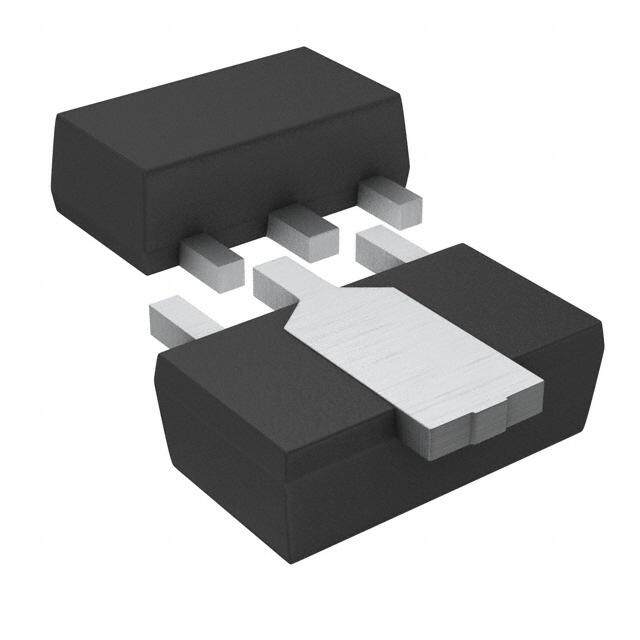
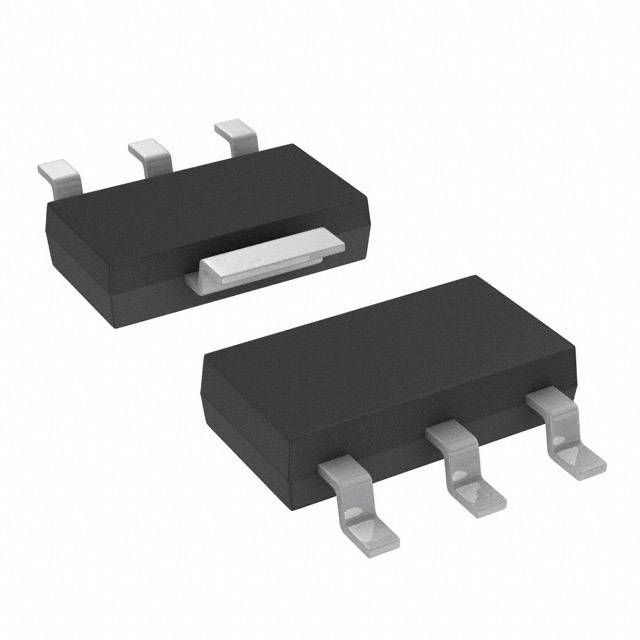
| 产品图片 |
|
| rohs | 符合RoHS无铅 / 符合限制有害物质指令(RoHS)规范要求 |
| 产品系列 | 晶体管,两极晶体管 - BJT,ROHM Semiconductor 2SD1898T100Q- |
| 数据手册 | |
| 产品型号 | 2SD1898T100Q |
| 不同 Ib、Ic时的 Vce饱和值(最大值) | 400mV @ 20mA,500mA |
| 不同 Ic、Vce 时的DC电流增益(hFE)(最小值) | 120 @ 500mA,3V |
| 产品目录绘图 |
|
| 产品目录页面 | |
| 产品种类 | 两极晶体管 - BJT |
| 供应商器件封装 | MPT3 |
| 其它名称 | 2SD1898T100QDKR |
| 功率-最大值 | 2W |
| 包装 | Digi-Reel® |
| 发射极-基极电压VEBO | 5 V |
| 商标 | ROHM Semiconductor |
| 增益带宽产品fT | 100 MHz |
| 安装类型 | 表面贴装 |
| 安装风格 | SMD/SMT |
| 封装 | Reel |
| 封装/外壳 | TO-243AA |
| 封装/箱体 | SOT-89 |
| 工厂包装数量 | 1000 |
| 晶体管极性 | NPN |
| 晶体管类型 | NPN |
| 最大功率耗散 | 0.5 W |
| 最大工作温度 | + 150 C |
| 最大直流电集电极电流 | 1 A |
| 最小工作温度 | - 55 C |
| 标准包装 | 1 |
| 电压-集射极击穿(最大值) | 80V |
| 电流-集电极(Ic)(最大值) | 1A |
| 电流-集电极截止(最大值) | - |
| 直流电流增益hFE最大值 | 390 |
| 直流集电极/BaseGainhfeMin | 82 |
| 配置 | Single |
| 集电极—发射极最大电压VCEO | 80 V |
| 集电极—基极电压VCBO | 120 V |
| 集电极连续电流 | 1 A |
| 频率-跃迁 | 100MHz |


- 商务部:美国ITC正式对集成电路等产品启动337调查
- 曝三星4nm工艺存在良率问题 高通将骁龙8 Gen1或转产台积电
- 太阳诱电将投资9.5亿元在常州建新厂生产MLCC 预计2023年完工
- 英特尔发布欧洲新工厂建设计划 深化IDM 2.0 战略
- 台积电先进制程称霸业界 有大客户加持明年业绩稳了
- 达到5530亿美元!SIA预计今年全球半导体销售额将创下新高
- 英特尔拟将自动驾驶子公司Mobileye上市 估值或超500亿美元
- 三星加码芯片和SET,合并消费电子和移动部门,撤换高东真等 CEO
- 三星电子宣布重大人事变动 还合并消费电子和移动部门
- 海关总署:前11个月进口集成电路产品价值2.52万亿元 增长14.8%


PDF Datasheet 数据手册内容提取
2SD1898 / 2SD1733 NPN 1.0A 80V Middle Power Transistor Datasheet lOutline Parameter Value MPT3 CPT3 Collector V 80V CEO Base r IC 1.0A Collector o Emitter Base Emitter f 2SD1898 2SD1733 lFeatures (SC-62) (SC-63) 1) Suitable for Middle Power Driver <SOT-89> d <SOT-428> 2) Complementary PNP Types : 2SB1260 / 2SB1181 e 3) Low V CE(sat) V = 0.4V Max. (I /I =500mA/20mA) CE(sat) C B d 4) Lead Free/RoHS Compliant. s n n e g lInner circuit m Collector i lApplicsations m Motor driver , LED driver Base e Power supply o D Emitter c w e R lPackaging specifications e Package Basic N Taping Reel size Tape width Part Nto. Package size ordering Marking code (mm) (mm) (mm) unit (pcs) o 2SD1898 MPT3 4540 T100 180 12 1,000 DF N 2SD1733 CPT3 6595 TL 330 16 2,500 D1733 www.rohm.com © 2013 ROHM Co., Ltd. All rights reserved. 1/7 2013.05 - Rev.F
2SD1898 / 2SD1733 Data Sheet lAbsolute maximum ratings (Ta = 25°C) Parameter Symbol Values Unit Collector-base voltage V 120 V CBO Collector-emitter voltage V 80 V CEO Emitter-base voltage V 5 V EBO r DC IC 1.0 o A Collector current Pulsed I *1 2.0 A CP f 0.5 *2 W 2SD1898 d 2.0 *3 W Power dissipation P D e 1 *4 W 2SD1733 d 10 *5 W Junction temperature Tj n 150s °C Range of storage temperature T -55 to +150 °C stg n e *1 Pw=20ms , duty=1/2 *2 Each terminal mounted on a reference land m g *3 Mounted on a ceramic board (40×40×0.7 mm) i *4 Mounted on a substrate s m *5 T =25°C C e lElectrical characteristics (Ta = 25°C) o D Parameter Symbol Conditions Min. Typ. Max. Unit c Collector-emitter BV I = 1mA 80 - - V breakdown voltage CEO Cw e Collector-base BV I = 50mA 120 - - V breakdown voltage R CBO C e Emitter-base BV I = 50mA 5 - - V breakdown vol tage EBO E N t Collector cut-off current I V = 100V - - 1 mA CBO CB o Emitter cut-off current I V = 4V - - 1 mA N EBO EB Collector-emitter V I = 500mA, I = 20mA - 0.15 0.40 V saturation voltage CE(sat) C B DC current gain h *6 V = 3V, I = 0.5A 120 - 390 - FE CE C V = 10V, I = -50mA Transition frequency f CE E - 100 - MHz T f=100MH Z V = 10V, I = 0A Output capacitance C CB E - 20 - pF ob f = 1MHz lh rank categories FE Rank Q R h 120 to 270 180 to 390 FE www.rohm.com © 2013 ROHM Co., Ltd. All rights reserved. 2/7 2013.05 - Rev.F
2SD1898 / 2SD1733 Data Sheet lElectrical characteristic curves(Ta = 25°C) Fig.1 Ground Emitter Propagation Characteristics Fig.2 Typical Output Characteristics 1000 r mA] VPCuEls=e 5dV A] o T : I[C 100 NT : I[C f N E E R R d R R U 10 U C OR C Ta=10205ººCC OR e CT -40ºC CT d E 1 E L L L OL O n s C C 0.1 0 0.5 1 1.5 e n g m BASE TO EMITTER VOLTAGE : V [V] COLECTOR TO EMITTE VOLTAGE : V [V] BE CE i s m e o Fig.3 DC Current Gain vs. Collector Current(I) FDig.4 DC Current Gain vs. Collector Current(II) c 1000 1000 VCE= 3V e w Ta=25ºC Pulsed Pulsed E E F F h R h N : e N : AI AI G G N NT 100 t NT 100 E E V = 3V R o Ta=100ºC R CE 1V R 25ºC R U U C -40ºC C N C C D D 10 10 1 10 100 1000 10000 1 10 100 1000 10000 COLLECTOR CURRENT : I [mA] COLLECTOR CURRENT : I [mA] C C www.rohm.com © 2013 ROHM Co., Ltd. All rights reserved. 3/7 2013.05 - Rev.F
2SD1898 / 2SD1733 Data Sheet lElectrical characteristic curves(Ta = 25°C) Fig.5 Collector-Emitter Saturation Voltage Fig.6 Collector-Emitter Saturation Voltage vs. Collector Current (I) vs. Collector Current (II) 1 1 r V] IC / IB = 20 V] Ta=25ºC [at) [at) o s s E( E( VC VC f R GE : R GE : d EA Ta=100ºC EA TTLT 0.1 25ºC TTLT 0.1 IC / IB =20/1 MIO -40ºC MIO e10/1 EV EV -N -N R R O O O O d TTI TTI CA CA ER ER s LU LU n LT LT OA OA CS CS n 0.01 0.e01 1 10 100 1000 10000 1 10 100 1000 10000 g m COLLECTOR CURRENT : I [mA] COLLECTOR CURRENT : I [mA] C C i s m e o Fig.7 Base-Emitter Saturation Voltage DFig.8 Gain Bandwidth Product vs. Collector Current vs. Emitter Current c 10 V] e w Hz] V [BE(sat) R e Y : f[MT E : Ta= -4250ººCC NC G E A 100ºC N U T 1 t Q L E R VO o FR EN N TO O MITTIN TI -ERA NSI EU A ASAT IC / IB = 20 TR BS 0.1 1 10 100 1000 10000 COLLECTOR CURRENT : I [mA] EMITTER CURRENT : I [mA] C E www.rohm.com © 2013 ROHM Co., Ltd. All rights reserved. 4/7 2013.05 - Rev.F
2SD1898 / 2SD1733 Data Sheet lElectrical characteristic curves(Ta = 25°C) Fig.9 Emitter input capacitance vs. Emitter-Base Voltage F] Collector output capacitance vs. Fig.10 Safe Operating Area p Collector-Base Voltage b [ 10 CE : Cob [pF] [A] C 2SD1898 1mos1 0mrs CITANCE : Ci NT : I 1 f AN E PA R d AT R UT CPACI R CU 0.1 100ems PA O DC TC T OUUT EC 0.01 d(reMfoeurenntecde olann da) R P LL ON O n s TR I C Ta=25ºC CE Single non repetitive pulse LETT 0.0e01 n OLMI 0.1 1 10 100 CE g COLLECTOR - BASE VOLTAGE : V [V] m CB COLLECTOR TO EMITTER VOLTAGE : V [V] EMITTER - BASE VOLTAGE : V [V] CE EB i s m e o Fig.11 Safe Operating Area D c 10 2SD1733 1ms A] e w [C 10ms T : I 1 R e N E R R N U 0.1 t C 100ms R o O T C DC EN 0.01 L L O C Ta=25ºC Single non repetitive pulse 0.001 0.1 1 10 100 COLLECTOR TO EMITTER VOLTAGE : V [V] CE www.rohm.com © 2013 ROHM Co., Ltd. All rights reserved. 5/7 2013.05 - Rev.F
2SD1898 / 2SD1733 Data Sheet lDimensions (Unit : mm) D b1 A MPT3 HE E r o E p L L f b2 c b x S A db4 e1 e e d β 3 l s n 1 l n e A b3 m g b5 2 l y S i e1 S s m e e Pattern of terminal position areas [Not a recommended pattern of soldering pads] o D cMILIMETERS INCHES DIM MIN MAX MIN MAX A e 1.40 1w.50 0.055 0.059 b 0.30 0.50 0.012 0.020 b1 1.50 1.70 0.059 0.067 R b2 0.40 e 0.60 0.016 0.024 c 0.35 0.50 0.014 0.020 D 4.40 4.70 0.173 0.185 N E 2.40 2.70 0.094 0.106 t e 3.00 0.118 o e1 1.50 0.059 HE 3.70 4.30 0.146 0.169 LE 0.80 1.20 0.031 0.047 N Lp 1.01 1.41 0.040 0.056 x - 0.15 - 0.006 y - 0.10 - 0.004 MILIMETERS INCHES DIM MIN MAX MIN MAX b3 - 0.65 - 0.026 b4 - 1.70 - 0.067 b5 - 0.75 - 0.030 l1 - 1.71 - 0.067 l2 - 0.58 - 0.023 l3 - 3.72 - 0.146 β 45° 45° Dimension in mm / inches www.rohm.com © 2013 ROHM Co., Ltd. All rights reserved. 6/7 2013.05 - Rev.F
2SD1898 / 2SD1733 Data Sheet lDimensions (Unit : mm) A2 D B A b1 c1 CPT3 2 L 3 L r E H A1 o 4 b2 L f b3 L dL1 Lp c e e b x B A A3 d l3 l2 l1n s e b5 n g 6 m b ie s m Pattern of terminal position areas [Not a recommended pattern of soeldering pads] o DIM MILIMETERS D INCHES MIN MAX MIN MAX A1 0c.00 0.15 0.000 0.006 A2 2.20 2.50 0.087 0.098 A3 0.25 0.010 w b e 0.55 0.75 0.022 0.030 b1 5.00 5.30 0.197 0.209 b2R 5.00 0.197 b3 0e.75 0.030 c 0.40 0.60 0.016 0.024 c1 0.40 0.60 0.016 0.024 N D 6.30 6.70 0.248 0.264 t E 5.40 5.80 0.213 0.228 o e 2.30 0.091 HE 9.00 10.00 0.354 0.394 L 2.20 2.80 0.087 0.110 N L1 0.80 1.40 0.031 0.055 L2 1.20 1.80 0.047 0.071 L3 5.30 0.209 L4 0.90 0.035 Lp 1.00 1.60 0.039 0.063 x - 0.25 - 0.010 MILIMETERS INCHES DIM MIN MAX MIN MAX b5 - 1.00 - 0.04 b6 - 5.20 - 0.205 l1 - 2.50 - 0.098 l2 - 5.50 - 0.217 l3 - 10.00 - 0.394 Dimension in mm / inches www.rohm.com © 2013 ROHM Co., Ltd. All rights reserved. 7/7 2013.05 - Rev.F
Notice Notes 1) The information contained herein is subject to change without notice. 2) Before you use our Products, please contact our sales representativeand verify the latest specifica- r tions : o 3) Although ROHM is continuously working to improve product reliability and quality, semicon- ductors can break down and malfunction due to various factors. Therefore, in order to prevent personal injury or fire arising from failure, please take fsafety measures such as complying with the derating characteristics, implementing redundant and fire prevention designs, and utilizing backups and fail-safe procedures. ROHM shall have no responsibility for any damages arising out of the use of our Poducts beyond the ratindg specified by ROHM. 4) Examples of application circuits, circuit constants and any other informatione contained herein are provided only to illustrate the standard usage and operations of the Products. The peripheral conditions must be taken into account when designing circuits for mass production. d 5) The technical information specified herein is intended only to show the typical functions of and examples of application circuits for the Products. ROHM does not grant you, explicitly or implicitly, any license to use or exercise intellectual property or othern rights held by ROHM or asny other parties. ROHM shall have no responsibility whatsoever for any dispute arising out of the use of such technical information. n e 6) The Products are intended for use in general electronic equipment (i.e. AV/OA devices, communi- cation, consumer systems, gaming/entertainment sets) as well as the applications indicated in this document. m g 7) The Products specified in this document are not designed to be radiation tolerant. i 8) For use of our Products in applications requiring a high desgree of reliability (as exemplified below), please contact and consult m with a ROHM representative : transportation equipment (i.e. cars, ships, trains), primary communication equipment, traffic lights, fire/crime prevention, safety equipment, medical systems, servers, solar cells, and poweer transmission systems. 9) Do not use our Products in applications requiring extremely high reliability, such as aerospace o equipment, nuclear power control systems, and suDbmarine repeaters. 10) ROHM shall have no responsibility for any damages or injury arising from non-compliance with c the recommended usage conditions and specifications contained herein. 11) ROHM has used reasonable care tow ensur the accuracy of the information contained in this e document. However, ROHM does not warrants that such information is error-free, and ROHM shall have no responsibility for any damages arising from any inaccuracy or misprint of such information. R e 12) Please use the Products in accordance with any applicable environmental laws and regulations, such as the RoHS Directive. For more details, including RoHS compatibility, please contact a ROHM sales office. ROHM shall have no responsibility for any damages or losses resulting N non-compliance with any applicable laws or regulations. t 13) When providing our Products and technologies contained in this document to other countries, o you must abide by the procedures and provisions stipulated in all applicable export laws and regulations, including without limitation the US Export Administration Regulations and the Foreign Exchange and Foreign Trade Act. N 14) This document, in part or in whole, may not be reprinted or reproduced without prior consent of ROHM. Thank you for your accessing to ROHM product informations. More detail product informations and catalogs are available, please contact us. ROHM Customer Support System http://www.rohm.com/contact/ www.rohm.com R1102A © 2013 ROHM Co., Ltd. All rights reserved.
Mouser Electronics Authorized Distributor Click to View Pricing, Inventory, Delivery & Lifecycle Information: R OHM Semiconductor: 2SD1733TLP 2SD1733TLQ 2SD1733TLR 2SD1898T100P 2SD1898T100Q 2SD1898T100R