ICGOO在线商城 > 分立半导体产品 > 晶体管 - 双极 (BJT) - 单 > MMBT100
 Datasheet下载
- 型号: MMBT100
- 制造商: Fairchild Semiconductor
- 库位|库存: xxxx|xxxx
- 要求:
| 数量阶梯 | 香港交货 | 国内含税 |
| +xxxx | $xxxx | ¥xxxx |
查看当月历史价格
查看今年历史价格
MMBT100产品简介:
ICGOO电子元器件商城为您提供MMBT100由Fairchild Semiconductor设计生产,在icgoo商城现货销售,并且可以通过原厂、代理商等渠道进行代购。 MMBT100价格参考¥0.64-¥3.90。Fairchild SemiconductorMMBT100封装/规格:晶体管 - 双极 (BJT) - 单, Bipolar (BJT) Transistor NPN 45V 500mA 250MHz 350mW Surface Mount SOT-23-3。您可以下载MMBT100参考资料、Datasheet数据手册功能说明书,资料中有MMBT100 详细功能的应用电路图电压和使用方法及教程。
ON Semiconductor的MMBT100是一款NPN型双极结型晶体管(BJT),采用SOT-23小型表面贴装封装,适用于空间受限的便携式电子设备。该器件具有较高的开关速度和良好的增益性能,常用于低电压、低电流的模拟放大和数字开关应用。

典型应用场景包括:便携式消费类电子产品中的信号放大与开关控制,如智能手机、平板电脑和可穿戴设备中的音频前置放大电路或小信号处理模块;在电源管理电路中作为低功耗开关元件,用于控制LED指示灯、继电器或传感器供电;还可用于各类小型电子设备中的逻辑电平转换和驱动电路,例如在微控制器与外围器件之间实现信号缓冲或驱动能力增强。

由于其封装小巧、可靠性高,MMBT100也广泛应用于通信设备、家用电器控制板、玩具电子模块及工业控制中的小型化设计。此外,在需要高频响应的射频(RF)前端电路中,该晶体管也可用于低噪声小信号放大。

总体而言,MMBT100凭借其优良的开关特性、紧凑的封装和稳定的性能,适合对空间和功耗敏感的中低功率电子系统,是通用模拟与数字电路设计中的常用元件。
| 参数 | 数值 |
| 产品目录 | |
| 描述 | TRANSISTOR NPN GP SOT-23两极晶体管 - BJT NPN Transistor General Purpose |
| 产品分类 | 晶体管(BJT) - 单路分离式半导体 |
| 品牌 | Fairchild Semiconductor |
| 产品手册 | |
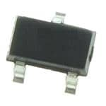
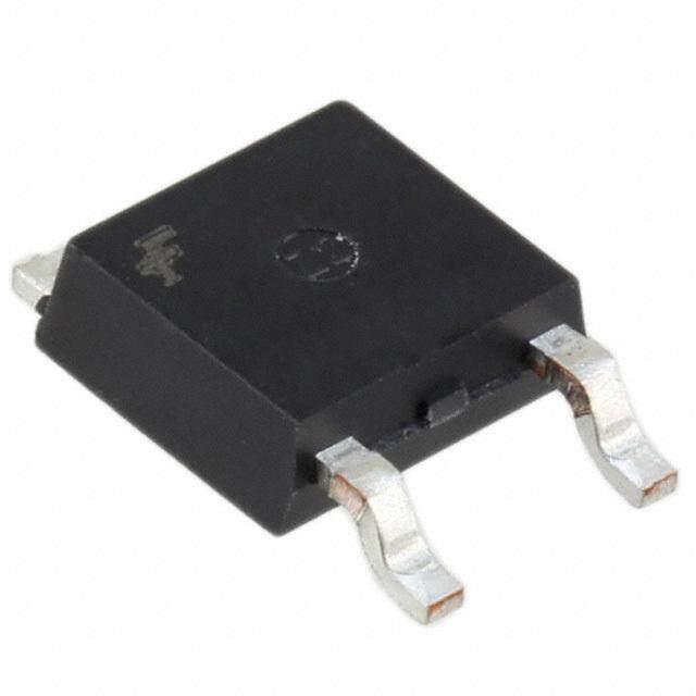
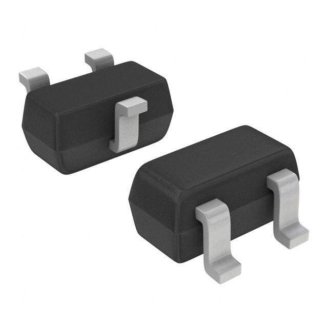
| 产品图片 |
|
| rohs | 符合RoHS无铅 / 符合限制有害物质指令(RoHS)规范要求 |
| 产品系列 | 晶体管,两极晶体管 - BJT,Fairchild Semiconductor MMBT100- |
| 数据手册 | |
| 产品型号 | MMBT100 |
| PCN封装 | |
| PCN组件/产地 | |
| PCN设计/规格 | |
| 不同 Ib、Ic时的 Vce饱和值(最大值) | 400mV @ 20mA,200mA |
| 不同 Ic、Vce 时的DC电流增益(hFE)(最小值) | 100 @ 150mA,5V |
| 产品种类 | 两极晶体管 - BJT |
| 供应商器件封装 | SOT-23-3 |
| 其它名称 | MMBT100DKR |
| 功率-最大值 | 350mW |
| 包装 | Digi-Reel® |
| 单位重量 | 60 mg |
| 发射极-基极电压VEBO | 6 V |
| 商标 | Fairchild Semiconductor |
| 增益带宽产品fT | 250 MHz |
| 安装类型 | 表面贴装 |
| 安装风格 | SMD/SMT |
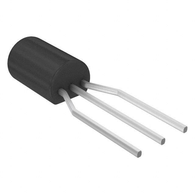
| 封装 | Reel |
| 封装/外壳 | TO-236-3,SC-59,SOT-23-3 |
| 封装/箱体 | SOT-23 |
| 工厂包装数量 | 3000 |
| 晶体管极性 | NPN |
| 晶体管类型 | NPN |
| 最大功率耗散 | 350 mW |
| 最大工作温度 | + 150 C |
| 最大直流电集电极电流 | 0.5 A |
| 最小工作温度 | - 55 C |
| 标准包装 | 1 |
| 电压-集射极击穿(最大值) | 45V |
| 电流-集电极(Ic)(最大值) | 500mA |
| 电流-集电极截止(最大值) | 50nA |
| 直流电流增益hFE最大值 | 450 |
| 直流集电极/BaseGainhfeMin | 100 |
| 系列 | MMBT100 |
| 配置 | Single |
| 集电极—发射极最大电压VCEO | 45 V |
| 集电极—基极电压VCBO | 75 V |
| 集电极—射极饱和电压 | 0.4 V |
| 集电极连续电流 | 0.5 A |
| 零件号别名 | MMBT100_NL |
| 频率-跃迁 | 250MHz |


- 商务部:美国ITC正式对集成电路等产品启动337调查
- 曝三星4nm工艺存在良率问题 高通将骁龙8 Gen1或转产台积电
- 太阳诱电将投资9.5亿元在常州建新厂生产MLCC 预计2023年完工
- 英特尔发布欧洲新工厂建设计划 深化IDM 2.0 战略
- 台积电先进制程称霸业界 有大客户加持明年业绩稳了
- 达到5530亿美元!SIA预计今年全球半导体销售额将创下新高
- 英特尔拟将自动驾驶子公司Mobileye上市 估值或超500亿美元
- 三星加码芯片和SET,合并消费电子和移动部门,撤换高东真等 CEO
- 三星电子宣布重大人事变动 还合并消费电子和移动部门
- 海关总署:前11个月进口集成电路产品价值2.52万亿元 增长14.8%


PDF Datasheet 数据手册内容提取
Is Now Part of To learn more about ON Semiconductor, please visit our website at www.onsemi.com Please note: As part of the Fairchild Semiconductor integration, some of the Fairchild orderable part numbers will need to change in order to meet ON Semiconductor’s system requirements. Since the ON Semiconductor product management systems do not have the ability to manage part nomenclature that utilizes an underscore (_), the underscore (_) in the Fairchild part numbers will be changed to a dash (-). This document may contain device numbers with an underscore (_). Please check the ON Semiconductor website to verify the updated device numbers. The most current and up-to-date ordering information can be found at www.onsemi.com. Please email any questions regarding the system integration to Fairchild_questions@onsemi.com. ON Semiconductor and the ON Semiconductor logo are trademarks of Semiconductor Components Industries, LLC dba ON Semiconductor or its subsidiaries in the United States and/or other countries. ON Semiconductor owns the rights to a number of patents, trademarks, copyrights, trade secrets, and other intellectual property. A listing of ON Semiconductor’s product/patent coverage may be accessed at www.onsemi.com/site/pdf/Patent-Marking.pdf. ON Semiconductor reserves the right to make changes without further notice to any products herein. ON Semiconductor makes no warranty, representation or guarantee regarding the suitability of its products for any particular purpose, nor does ON Semiconductor assume any liability arising out of the application or use of any product or circuit, and specifically disclaims any and all liability, including without limitation special, consequential or incidental damages. Buyer is responsible for its products and applications using ON Semiconductor products, including compliance with all laws, regulations and safety requirements or standards, regardless of any support or applications information provided by ON Semiconductor. “Typical” parameters which may be provided in ON Semiconductor data sheets and/or specifications can and do vary in different applications and actual performance may vary over time. All operating parameters, including “Typicals” must be validated for each customer application by customer’s technical experts. ON Semiconductor does not convey any license under its patent rights nor the rights of others. ON Semiconductor products are not designed, intended, or authorized for use as a critical component in life support systems or any FDA Class 3 medical devices or medical devices with a same or similar classification in a foreign jurisdiction or any devices intended for implantation in the human body. Should Buyer purchase or use ON Semiconductor products for any such unintended or unauthorized application, Buyer shall indemnify and hold ON Semiconductor and its officers, employees, subsidiaries, affiliates, and distributors harmless against all claims, costs, damages, and expenses, and reasonable attorney fees arising out of, directly or indirectly, any claim of personal injury or death associated with such unintended or unauthorized use, even if such claim alleges that ON Semiconductor was negligent regarding the design or manufacture of the part. ON Semiconductor is an Equal Opportunity/Affirmative Action Employer. This literature is subject to all applicable copyright laws and is not for resale in any manner.
P N 1 0 October 2008 0 / P N 1 PN100/PN100A/MMBT100/MMBT100A 0 0 A NPN General Purpose Amplifier / M M • This device is designed for general purpose amplifier applications at collector currents to 300mA. B • Sourced from process 10. T 1 0 0 / M C M B T E 1 0 1 TO-92 B SOT-23 0A 1. Emitter 2. Base 3. Collector — Mark: PN100/PN100A N P Absolute Maximum Ratings* N Ta = 25°C unless otherwise noted G e Symbol Parameter Ratings Units n e V Collector-Emitter Voltage 45 CEO r a VCBO Collector-Base Voltage 75 l V Emitter-Base Voltage 6.0 P EBO u IC Collector current - Continuous 500 rp TJ, Tstg Junction and Storage Temperature -55 ~ +150 o s e * These ratings are limiting values above which the serviceability of any semiconductor device may be impaired. A NOTES: m 1. These ratings are based on a maximum junction temperature of 150 degrees C. p 2. These are steady state limits. The factory should be consulted on applications involving pulsed or low duty cycle operations. l i * Pulse Test: Pulse Width≤300μs, Duty Cycle≤2% f i e r Thermal Characteristics T =25°C unless otherwise noted A Max. Symbol Parameter PN100 *MMBT100 Units PN100A *MMBT100A P Total Device Dissipation 625 350 mW D Derate above 25°C 5.0 2.8 mW/°C R Thermal Resistance, Junction to Case 83.3 °C/W θJC R Thermal Resistance, Junction to Ambient 200 357 °C/W θJA * Device mounted on FR-4 PCB 1.6” × 1.6” × 0.06." © 2008 Fairchild Semiconductor Corporation www.fairchildsemi.com PN100/PN100A/MMBT100/MMBT100A Rev. C1 1
P N Electrical Characteristics T =25°C unless otherwise noted 1 C 0 0 Symbol Parameter Test Condition Min. Max. Units / P Off Characteristics N BV Collector-Base Breakdown Voltage I = 10μA, I = 0 75 V 1 CBO C E 0 BVCEO Collector-Emitter Breakdown Voltage * IC = 1mA, IB = 0 45 V 0 A BV Emitter-Base Breakdown Voltage I = 10μA, I = 0 6.0 V EBO E C / M I Collector-Base Cutoff Current V = 60V 50 nA CBO CB M I Collector-Emiitter Cutoff Current V = 40V 50 nA CES CE B I Emitter Cutoff Current V = 4V 50 nA T EBO EB 1 On Characteristics 0 0 h DC Current Gain I = 100μA, V = 1.0V 100 80 FE C CE / M 100A 240 M I = 10mA, V = 1.0V 100 100 450 C CE B 100A 300 600 T IC = 100mA, VCE = 1.0V* 100 1 I = 150mA, V = 5.0V * 100 100 350 0 C CE 0 100A 100 A VCE(sat) Collector-Emitter Saturation Voltage IC = 10mA, IB = 1.0mA 0.2 V — I = 200mA, I = 20mA 0.4 V C B N V Base-Emitter Saturation Voltage I = 10mA, I = 1.0mA 0.85 V BE(sat) C B P IC = 200mA, IB = 20mA 1.0 V N Small Signal Characteristics G f Current Gain Bandwidth Product V = 20V, I = 20mA 250 MHz e T CE C n Cobo Output Capacitance VCB = 5.0V, f = 1.0MHz 4.5 pF e r NF Noise Figure IC = 100μA, VCE = 5.0V 100 5.0 dB a RG = 2.0kΩ, f = 1.0KHz 100A 4.0 dB l P * Pulse Test: Pulse Width ≤ 300μs, Duty Cycle ≤ 2.0% u r p o s e A m p l i f i e r © 2008 Fairchild Semiconductor Corporation www.fairchildsemi.com PN100/PN100A/MMBT100/MMBT100A Rev. C1 2
P N Typical Characteristics 1 0 0 / P N T GAIN400 vs Collector Current Vce = 5V AGE (V)0.4 Voltage vs Collector Current 100A URREN300 125 °C R VOLT0.3 β = 10 /MM LSED C200 25 °C EMITTE0.2 25 °C BT10 L PU - 40 °C TOR- 0/M A100 C 125 °C h - TYPICFE 010 2I0 C - C3O0LLEC50TOR CU1R00RENT 2(m00A)300 500 V - COLLECESAT0.11 I C - COLL1E0CTOR CURRENT1 0(m0 -A 4)0 °C 400 MBT100 A Figure 1. Typical Pulsed Current Gain Figure 2. Collector-Emitter Saturation Voltage — vs Collector Current vs Collector Current N P Base-Emitter Saturation N Collector Current V) Voltage vs Collector Current V) G E ( E ( e AG AG 1 n LT 1 LT e O O r TTER V0.8 - 40 °C R ON V0.8 - 40 °C al Pu OR-EMI0.6 25 °C 125 °C MITTE0.6 25 °C 125 °C rpo V - COLLECTBESAT00..240.1 I C - C1OLLECTOR CU1R0RENT (mβA )=1 1000 300 V - BASE-EBEON00..24 1 I C - CVO CL EL E=C 51TV0OR CURRENT 1(m00A) 500 se Amplifie r Figure 3. Base-Emitter Saturation Voltage Figure 4. Base-Emitter On Voltage vs Collector Current vs Collector Current 100 A) 10 T (n V C B = 60V f = 1.0 MHz EN F) R p CUR CE ( 10 Cib CTOR 1 CITAN Cob LE PA 1 L A O C C I - CBO0.1 0.1 25 50 75 100 125 150 0.1 1 10 100 TA - AMBIENT TEMPERATURE ( ° C) Vc e - COLLECTOR VOLTAGE (V) Figure 5. Collector Cutoff Current Figure 6. Input and Output Capacitance vs Ambient Temperature vs Reverse Voltag © 2008 Fairchild Semiconductor Corporation www.fairchildsemi.com PN100/PN100A/MMBT100/MMBT100A Rev. C1 3
P N Typical Characteristics 1 (Continued) 0 0 / P N 300 700 1 270 ts mW)600 00 221400 ON (500 TO-92 A/M E (nS)115800 IB1V = c Ic B 2= =1 0Ic V / 10 SSIPATI400 SOT-23 MB TIM120 R DI300 T1 90 tf tr OWE200 00 60 P / 30 td P - D100 MM 010 20 30 50 100 200 300 00 25 50 75 100 125 150 B I C - COLLECTOR CURRENT (mA) TEMPERATURE ( o C) T1 0 Figure 7. Switching Times vs Figure 8. Power Dissipation vs 0 A Collector Current Ambient Temperature — N P N G e n e r a l P u r p o s e A m p l i f i e r © 2008 Fairchild Semiconductor Corporation www.fairchildsemi.com PN100/PN100A/MMBT100/MMBT100A Rev. C1 4
P N Package Dimension (TO92) 1 0 0 / P N 1 0 0 A / M M B T 1 0 0 / M M B T 1 0 0 A — N P N G e n e r a l P u r p o s e A m p l i f i e r © 2008 Fairchild Semiconductor Corporation www.fairchildsemi.com PN100/PN100A/MMBT100/MMBT100A Rev. C1 5
P N Package Dimension (SOT23) 1 0 0 / P N 1 0 0 A / M M B T 1 0 0 / M M B T 1 0 0 A — N P N G e n e r a l P u r p o s e A m p l i f i e r © 2008 Fairchild Semiconductor Corporation www.fairchildsemi.com PN100/PN100A/MMBT100/MMBT100A Rev. C1 6
PP NN 11 00 00 // PP NN 11 00 00 TRADEMARKS AA The following are registered and unregistered trademarks and service marks Fairchild Semiconductor owns or is authorized to use and // MM is not intended to be an exhaustive list of all such trademarks. MM ACEx® Green FPS™ Power247® SuperSOT™-8 BB Build it Now™ Green FPS™ e-Series™ POWEREDGE® SyncFET™ TT CorePLUS™ GTO™ Power-SPM™ The Power Franchise® 11 00 CROSSVOLT™ i-Lo™ PowerTrench® 00 CTL™ IntelliMAX™ Programmable Active Droop™ /M/M Current Transfer Logic™ ISOPLANAR™ QFET® TinyBoost™ MM EcoSPARK® MegaBuck™ QS™ TinyBuck™ BB MICROCOUPLER™ QT Optoelectronics™ TinyLogic® TT Fairchild® MicroFET™ Quiet Series™ TINYOPTO™ 11 00 Fairchild Semiconductor® MicroPak™ RapidConfigure™ TinyPower™ 00 AA FACT Quiet Series™ MillerDrive™ SMART START™ TinyPWM™ FACT® Motion-SPM™ SPM® TinyWire™ N FAST® OPTOLOGIC® STEALTH™ µSerDes™ P FastvCore™ OPTOPLANAR® SuperFET™ UHC® N FPS™ ® SuperSOT™-3 UniFET™ G FRFET® PDP-SPM™ SuperSOT™-6 VCX™ e Global Power ResourceSM Power220® n e r a l P DISCLAIMER u FAIRCHILD SEMICONDUCTOR RESERVES THE RIGHT TO MAKE CHANGES WITHOUT FURTHER NOTICE TO ANY PRODUCTS r p HEREIN TO IMPROVE RELIABILITY, FUNCTION, OR DESIGN. FAIRCHILD DOES NOT ASSUME ANY LIABILITY ARISING OUT OF o THE APPLICATION OR USE OF ANY PRODUCT OR CIRCUIT DESCRIBED HEREIN; NEITHER DOES IT CONVEY ANY LICENSE s e UNDER ITS PATENT RIGHTS, NOR THE RIGHTS OF OTHERS. THESE SPECIFICATIONS DO NOT EXPAND THE TERMS OF A FAIRCHILD’S WORLDWIDE TERMS AND CONDITIONS, SPECIFICALLY THE WARRANTY THEREIN, WHICH COVERS THESE m PRODUCTS. p l i f i LIFE SUPPORT POLICY e r FAIRCHILD’S PRODUCTS ARE NOT AUTHORIZED FOR USE AS CRITICAL COMPONENTS IN LIFE SUPPORT DEVICES OR SYSTEMS WITHOUT THE EXPRESS WRITTEN APPROVAL OF FAIRCHILD SEMICONDUCTOR CORPORATION. As used herein: 1. Life support devices or systems are devices or systems 2. A critical component is any component of a life support which, (a) are intended for surgical implant into the body, or device or system whose failure to perform can be reasonably (b) support or sustain life, and (c) whose failure to perform expected to cause the failure of the life support device or when properly used in accordance with instructions for use system, or to affect its safety or effectiveness. provided in the labeling, can be reasonably expected to result in significant injury to the user. PRODUCT STATUS DEFINITIONS Definition of Terms Datasheet Identification Product Status Definition This datasheet contains the design specifications for product development. Advance Information Formative or In Design Specifications may change in any manner without notice. This datasheet contains preliminary data; supplementary data will be pub- Preliminary First Production lished at a later date. Fairchild Semiconductor reserves the right to make changes at any time without notice to improve design. This datasheet contains final specifications. Fairchild Semiconductor reserves No Identification Needed Full Production the right to make changes at any time without notice to improve design. This datasheet contains specifications on a product that has been discontin- Obsolete Not In Production ued by Fairchild semiconductor. The datasheet is printed for reference infor- mation only. Rev. I31 © 2008 Fairchild Semiconductor Corporation www.fairchildsemi.com PN100/PN100A/MMBT100/MMBT100A Rev. C1 7
ON Semiconductor and are trademarks of Semiconductor Components Industries, LLC dba ON Semiconductor or its subsidiaries in the United States and/or other countries. ON Semiconductor owns the rights to a number of patents, trademarks, copyrights, trade secrets, and other intellectual property. A listing of ON Semiconductor’s product/patent coverage may be accessed at www.onsemi.com/site/pdf/Patent−Marking.pdf. ON Semiconductor reserves the right to make changes without further notice to any products herein. ON Semiconductor makes no warranty, representation or guarantee regarding the suitability of its products for any particular purpose, nor does ON Semiconductor assume any liability arising out of the application or use of any product or circuit, and specifically disclaims any and all liability, including without limitation special, consequential or incidental damages. Buyer is responsible for its products and applications using ON Semiconductor products, including compliance with all laws, regulations and safety requirements or standards, regardless of any support or applications information provided by ON Semiconductor. “Typical” parameters which may be provided in ON Semiconductor data sheets and/or specifications can and do vary in different applications and actual performance may vary over time. All operating parameters, including “Typicals” must be validated for each customer application by customer’s technical experts. ON Semiconductor does not convey any license under its patent rights nor the rights of others. ON Semiconductor products are not designed, intended, or authorized for use as a critical component in life support systems or any FDA Class 3 medical devices or medical devices with a same or similar classification in a foreign jurisdiction or any devices intended for implantation in the human body. Should Buyer purchase or use ON Semiconductor products for any such unintended or unauthorized application, Buyer shall indemnify and hold ON Semiconductor and its officers, employees, subsidiaries, affiliates, and distributors harmless against all claims, costs, damages, and expenses, and reasonable attorney fees arising out of, directly or indirectly, any claim of personal injury or death associated with such unintended or unauthorized use, even if such claim alleges that ON Semiconductor was negligent regarding the design or manufacture of the part. ON Semiconductor is an Equal Opportunity/Affirmative Action Employer. This literature is subject to all applicable copyright laws and is not for resale in any manner. PUBLICATION ORDERING INFORMATION LITERATURE FULFILLMENT: N. American Technical Support: 800−282−9855 Toll Free ON Semiconductor Website: www.onsemi.com Literature Distribution Center for ON Semiconductor USA/Canada 19521 E. 32nd Pkwy, Aurora, Colorado 80011 USA Europe, Middle East and Africa Technical Support: Order Literature: http://www.onsemi.com/orderlit Phone: 303−675−2175 or 800−344−3860 Toll Free USA/Canada Phone: 421 33 790 2910 Fax: 303−675−2176 or 800−344−3867 Toll Free USA/Canada Japan Customer Focus Center For additional information, please contact your local Email: orderlit@onsemi.com Phone: 81−3−5817−1050 Sales Representative © Semiconductor Components Industries, LLC www.onsemi.com www.onsemi.com 1
Mouser Electronics Authorized Distributor Click to View Pricing, Inventory, Delivery & Lifecycle Information: O N Semiconductor: MMBT100