ICGOO在线商城 > 分立半导体产品 > 晶体管 - 双极 (BJT) - 单 > KSH127TF

 Datasheet下载
- 型号: KSH127TF
- 制造商: Fairchild Semiconductor
- 库位|库存: xxxx|xxxx
- 要求:
| 数量阶梯 | 香港交货 | 国内含税 |
| +xxxx | $xxxx | ¥xxxx |
查看当月历史价格
查看今年历史价格
KSH127TF产品简介:
ICGOO电子元器件商城为您提供KSH127TF由Fairchild Semiconductor设计生产,在icgoo商城现货销售,并且可以通过原厂、代理商等渠道进行代购。 KSH127TF价格参考¥询价-¥询价。Fairchild SemiconductorKSH127TF封装/规格:晶体管 - 双极 (BJT) - 单, 双极 (BJT) 晶体管 PNP - 达林顿 100V 8A 1.75W 表面贴装 D-Pak。您可以下载KSH127TF参考资料、Datasheet数据手册功能说明书,资料中有KSH127TF 详细功能的应用电路图电压和使用方法及教程。
KSH127TF 是由 ON Semiconductor(安森美半导体)生产的一款双极型晶体管(BJT),属于单晶体管类型。该型号的应用场景主要包括以下方面:

1. 开关电路:KSH127TF 可用于各种开关电路中,例如继电器驱动、LED 驱动或小型电机控制等。其作为开关元件,在数字电路中实现信号的开与关。

2. 信号放大:作为一种双极型晶体管,KSH127TF 可用于音频信号放大器或其他低功率信号放大的场合。它能够将微弱的输入信号放大到更高的幅度,适用于消费电子设备中的音频处理部分。

3. 电源管理:在一些简单的电源管理系统中,如电池充电保护电路或电压调节器,KSH127TF 可以起到关键作用。它可以用来控制电流流动,确保设备获得稳定的工作电压。

4. 传感器接口:在工业自动化和物联网领域,KSH127TF 常被用作传感器信号调理的一部分。例如,将来自温度、压力或光敏传感器的小信号进行放大后传输给主控单元。

5. 脉宽调制 (PWM) 控制:在需要精确控制输出功率的应用中,如直流电机速度控制或 LED 亮度调节,KSH127TF 能够通过 PWM 技术实现高效的能量转换。

6. 通信设备:在某些低频通信系统中,该晶体管可用于构建调制解调电路或者数据传输链路中的缓冲级。

总结来说,KSH127TF 因其性能特点适合应用于中小功率范围内的电子电路设计中,尤其是在需要执行开关功能或小信号放大的地方。具体使用时需根据实际需求选择合适的外围电路配置,并参考官方提供的规格书以确保最佳工作状态。
| 参数 | 数值 |
| 产品目录 | |
| 描述 | TRANSISTOR PNP 100V 8A DPAK达林顿晶体管 PNP Silicon Darl |
| 产品分类 | 晶体管(BJT) - 单路分离式半导体 |
| 品牌 | Fairchild Semiconductor |
| 产品手册 | |
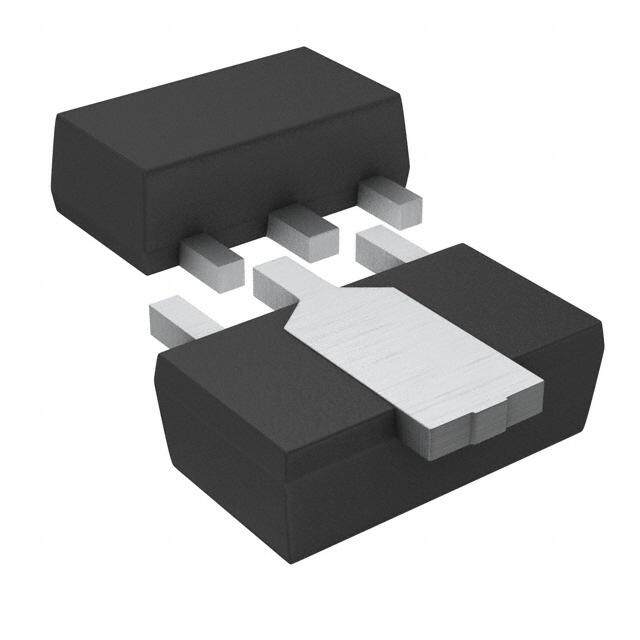
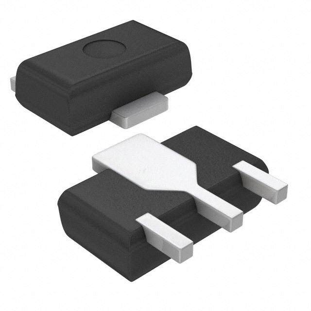
| 产品图片 |
|
| rohs | 符合RoHS无铅 / 符合限制有害物质指令(RoHS)规范要求 |
| 产品系列 | 晶体管,达林顿晶体管,Fairchild Semiconductor KSH127TF- |
| 数据手册 | |
| 产品型号 | KSH127TF |
| PCN封装 | |
| 不同 Ib、Ic时的 Vce饱和值(最大值) | 4V @ 80mA,8A |
| 不同 Ic、Vce 时的DC电流增益(hFE)(最小值) | 1000 @ 4A,4V |
| 产品目录页面 | |
| 产品种类 | |
| 供应商器件封装 | D-Pak |
| 其它名称 | KSH127TFCT |
| 功率-最大值 | 1.75W |
| 包装 | 剪切带 (CT) |
| 单位重量 | 260.370 mg |
| 发射极-基极电压VEBO | 5 V |
| 商标 | Fairchild Semiconductor |
| 安装类型 | 表面贴装 |
| 安装风格 | SMD/SMT |
| 封装 | Reel |
| 封装/外壳 | TO-252-3,DPak(2 引线+接片),SC-63 |
| 封装/箱体 | TO-252 |
| 工厂包装数量 | 2000 |
| 晶体管极性 | PNP |
| 晶体管类型 | PNP - 达林顿 |
| 最大工作温度 | + 150 C |
| 最大直流电集电极电流 | 8 A |
| 最大集电极截止电流 | 10 uA |
| 最小工作温度 | - 65 C |
| 标准包装 | 1 |
| 电压-集射极击穿(最大值) | 100V |
| 电流-集电极(Ic)(最大值) | 8A |
| 电流-集电极截止(最大值) | 10µA |
| 直流集电极/BaseGainhfeMin | 100 |
| 系列 | KSH127 |
| 配置 | Single |
| 集电极—发射极最大电压VCEO | 100 V |
| 集电极—基极电压VCBO | 100 V |
| 零件号别名 | KSH127TF_NL |
| 频率-跃迁 | - |


- 商务部:美国ITC正式对集成电路等产品启动337调查
- 曝三星4nm工艺存在良率问题 高通将骁龙8 Gen1或转产台积电
- 太阳诱电将投资9.5亿元在常州建新厂生产MLCC 预计2023年完工
- 英特尔发布欧洲新工厂建设计划 深化IDM 2.0 战略
- 台积电先进制程称霸业界 有大客户加持明年业绩稳了
- 达到5530亿美元!SIA预计今年全球半导体销售额将创下新高
- 英特尔拟将自动驾驶子公司Mobileye上市 估值或超500亿美元
- 三星加码芯片和SET,合并消费电子和移动部门,撤换高东真等 CEO
- 三星电子宣布重大人事变动 还合并消费电子和移动部门
- 海关总署:前11个月进口集成电路产品价值2.52万亿元 增长14.8%


PDF Datasheet 数据手册内容提取
Is Now Part of To learn more about ON Semiconductor, please visit our website at www.onsemi.com Please note: As part of the Fairchild Semiconductor integration, some of the Fairchild orderable part numbers will need to change in order to meet ON Semiconductor’s system requirements. Since the ON Semiconductor product management systems do not have the ability to manage part nomenclature that utilizes an underscore (_), the underscore (_) in the Fairchild part numbers will be changed to a dash (-). This document may contain device numbers with an underscore (_). Please check the ON Semiconductor website to verify the updated device numbers. The most current and up-to-date ordering information can be found at www.onsemi.com. Please email any questions regarding the system integration to Fairchild_questions@onsemi.com. ON Semiconductor and the ON Semiconductor logo are trademarks of Semiconductor Components Industries, LLC dba ON Semiconductor or its subsidiaries in the United States and/or other countries. ON Semiconductor owns the rights to a number of patents, trademarks, copyrights, trade secrets, and other intellectual property. A listing of ON Semiconductor’s product/patent coverage may be accessed at www.onsemi.com/site/pdf/Patent-Marking.pdf. ON Semiconductor reserves the right to make changes without further notice to any products herein. ON Semiconductor makes no warranty, representation or guarantee regarding the suitability of its products for any particular purpose, nor does ON Semiconductor assume any liability arising out of the application or use of any product or circuit, and specifically disclaims any and all liability, including without limitation special, consequential or incidental damages. Buyer is responsible for its products and applications using ON Semiconductor products, including compliance with all laws, regulations and safety requirements or standards, regardless of any support or applications information provided by ON Semiconductor. “Typical” parameters which may be provided in ON Semiconductor data sheets and/or specifications can and do vary in different applications and actual performance may vary over time. All operating parameters, including “Typicals” must be validated for each customer application by customer’s technical experts. ON Semiconductor does not convey any license under its patent rights nor the rights of others. ON Semiconductor products are not designed, intended, or authorized for use as a critical component in life support systems or any FDA Class 3 medical devices or medical devices with a same or similar classification in a foreign jurisdiction or any devices intended for implantation in the human body. Should Buyer purchase or use ON Semiconductor products for any such unintended or unauthorized application, Buyer shall indemnify and hold ON Semiconductor and its officers, employees, subsidiaries, affiliates, and distributors harmless against all claims, costs, damages, and expenses, and reasonable attorney fees arising out of, directly or indirectly, any claim of personal injury or death associated with such unintended or unauthorized use, even if such claim alleges that ON Semiconductor was negligent regarding the design or manufacture of the part. ON Semiconductor is an Equal Opportunity/Affirmative Action Employer. This literature is subject to all applicable copyright laws and is not for resale in any manner.
K S H 1 2 7 KSH127 D-PAK for Surface Mount Applications • High DC Current Gain • Built-in a Damper Diode at E-C • Lead Formed for Surface Mount Applications (No Suffix) • Straight Lead (I-PAK, “ - I “ Suffix) 1 D-PAK 1 I-PAK • Electrically Similar to Popular TIP127 • Complement to KSH122 1.Base 2.Collector 3.Emitter PNP Silicon Darlington Transistor Absolute Maximum Ratings T =25°C unless otherwise noted Equivalent Circuit C C Symbol Parameter Value Units V Collector-Base Voltage - 100 V CBO V Collector-Emitter Voltage - 100 V CEO B V Emitter-Base Voltage - 5 V EBO I Collector Current (DC) - 8 A C I Collector Current (Pulse) - 16 A CP I Base Current - 120 mA B R1 R2 P Collector Dissipation (T =25°C) 20 W C C R1≅8kΩ E Collector Dissipation (Ta=25°C) 1.75 W R2≅0.12kΩ T Junction Temperature 150 °C J T Storage Temperature - 65 ~ 150 °C STG Electrical Characteristics T =25°C unless otherwise noted C Symbol Parameter Test Condition Min. Max. Units V (sus) *Collector-Emitter Sustaining Voltage I = - 30mA, I = 0 - 100 V CEO C B I Collector Cut-off Current V = - 50V, I = 0 - 10 µA CEO CE B I Collector Cut-off Current V = - 100V, I = 0 - 10 µA CBO CB E I Emitter Cut-off Current V = - 5V, I = 0 - 2 mA EBO EB C h *DC Current Gain V = - 4V, I = - 4A 1000 12K FE CE C V = - 4V, V = -8A 100 CE EB V (sat) *Collector-Emitter Saturation Voltage I = - 4A, I = - 16mA - 2 V CE C B I = - 8A, I = - 80mA - 4 V C B V (sat) *Base-Emitter Saturation Voltage I = - 8A, I = - 80mA - 4.5 V BE C B V (on) *Base-Emitter On Voltage V = -4V, I = - 4A - 2.8 V BE CE C C Output Capacitance V = - 10V, I = 0 300 pF ob CB E f= 0.1MHz * Pulse Test: PW≤300µs, Duty Cycle≤2% ©2002 Fairchild Semiconductor Corporation Rev. A4, October 2002
K Typical Characteristics S H 1 2 7 10k GE -10 VCE = -4V TA IC = 250 IB L O V N VBE(sat) N O GAI ATI -1 C CURRENT 1k at)[V], SATUR -0.1 VCE(sat) h, DFE at), V(sCE 100 V(sBE -0.01 -0.1 -1 -10 -0.1 -1 -10 -100 IC[A], COLLECTOR CURRENT IC[A], COLLECTOR CURRENT Figure 1. DC current Gain Figure 2. Base-Emitter Saturation Voltage Collector-Emitter Saturation Voltage 1000 10 V = -30V IC=C 250I IC= -I B B1 B2 NCE 100 TIME 1 A N CIT N O tR A R C[pF], CAPob 10 µt,t [s], TURD 0.1 tD, VBE(off)=0 1 -0.1 -1 -10 -100 0.01 -0.1 -1 -10 VCB[V], COLLECTOR BASE VOLTAGE IC[A], COLLECTOR CURRENT Figure 3. Collector Output Capacitance Figure 4. Turn On Time 10 -100 V = -30V IC=C 250I µs], TURN OFF TIME 1 tSTG ICB1= -IB2B LECTOR CURRENT -1-10 DC5m1sm5s001µ0s0µs t,t [STGF tF A], COL -0.1 I[C -0.01 0.1 -1 -10 -100 -1000 -0.1 -1 -10 I[A], COLLECTOR CURRENT VCE[V], COLLECTOR-EMITTER VOLTAGE C Figure 5. Turn Off Time Figure 6. Safe Operating Area ©2002 Fairchild Semiconductor Corporation Rev. A4, October 2002
K Typical Characteristic (Continued) S H 1 2 7 25 N 20 O TI A P SI 15 S DI R WE 10 O P W], P[C 5 0 0 25 50 75 100 125 150 175 TC[oC], CASE TEMPERATURE Figure 7. Power Derating ©2002 Fairchild Semiconductor Corporation Rev. A4, October 2002
K Package Dimensions S H 1 2 7 D-PAK 6.60 ±0.20 5.34 ±0.30 0.20 2.30 ±0.10 ± (0.50) (4.34) (0.50) 0.70 0.50 ±0.10 0 2 0.20±0.60 0. ±2.70 0.20 ±6.10 0.20 ±9.50 0.30 ±0.91 0.10 N0.55 ±0 MI 8 0. 0 1 0. MAX0.96 0.76 ±0.10 ±89 0.50 ±0.10 0. 2.30TYP 2.30TYP 1.02 ±0.20 [2.30±0.20] [2.30±0.20] 2.30 ±0.20 6.60 ±0.20 (5.34) (5.04) 0) 0) 0) 7 9 0 (1.50) 0. 0. 1. ( ( ( ±9.50 0.30 ±6.10 0.20 ±2.70 0.20 (2XR0.25) 0.10)(3.05) ( 0.76 ±0.10 Dimensions in Millimeters ©2002 Fairchild Semiconductor Corporation Rev. A4, October 2002
K Package Dimensions (Continued) S H 1 2 7 I-PAK 6.60 ±0.20 2.30 ±0.20 5.34 ±0.20 (0.50) (4.34) (0.50) 0.50 ±0.10 0 2 ±0 0. ±0.20 0.20 0.6 70 ±0 0. 6.1 0 1 0 ±0. 0.3 80 ±0 0. 0.20 16.1 MAX0.96 ±0 30 8 0. 1. ±0 3 0.76 ±0.10 9. 2.30TYP 2.30TYP 0.50 ±0.10 [2.30±0.20] [2.30±0.20] Dimensions in Millimeters ©2002 Fairchild Semiconductor Corporation Rev. A4, October 2002
TRADEMARKS The following are registered and unregistered trademarks Fairchild Semiconductor owns or is authorized to use and is not intended to be an exhaustive list of all such trademarks. ACEx™ FACT™ ImpliedDisconnect™ PACMAN™ SPM™ ActiveArray™ FACT Quiet series™ ISOPLANAR™ POP™ Stealth™ Bottomless™ FAST® LittleFET™ Power247™ SuperSOT™-3 CoolFET™ FASTr™ MicroFET™ PowerTrench® SuperSOT™-6 CROSSVOLT™ FRFET™ MicroPak™ QFET™ SuperSOT™-8 DOME™ GlobalOptoisolator™ MICROWIRE™ QS™ SyncFET™ EcoSPARK™ GTO™ MSX™ QT Optoelectronics™ TinyLogic™ E2CMOS™ HiSeC™ MSXPro™ Quiet Series™ TruTranslation™ EnSigna™ I2C™ OCX™ RapidConfigure™ UHC™ Across the board. Around the world.™ OCXPro™ RapidConnect™ UltraFET® The Power Franchise™ OPTOLOGIC® SILENT SWITCHER® VCX™ Programmable Active Droop™ OPTOPLANAR™ SMART START™ DISCLAIMER FAIRCHILD SEMICONDUCTOR RESERVES THE RIGHT TO MAKE CHANGES WITHOUT FURTHER NOTICE TO ANY PRODUCTS HEREIN TO IMPROVE RELIABILITY, FUNCTION OR DESIGN. FAIRCHILD DOES NOT ASSUME ANY LIABILITY ARISING OUT OF THE APPLICATION OR USE OF ANY PRODUCT OR CIRCUIT DESCRIBED HEREIN; NEITHER DOES IT CONVEY ANY LICENSE UNDER ITS PATENT RIGHTS, NOR THE RIGHTS OF OTHERS. LIFE SUPPORT POLICY FAIRCHILD’S PRODUCTS ARE NOT AUTHORIZED FOR USE AS CRITICAL COMPONENTS IN LIFE SUPPORT DEVICES OR SYSTEMS WITHOUT THE EXPRESS WRITTEN APPROVAL OF FAIRCHILD SEMICONDUCTOR CORPORATION. As used herein: 1. Life support devices or systems are devices or systems 2. A critical component is any component of a life support which, (a) are intended for surgical implant into the body, device or system whose failure to perform can be or (b) support or sustain life, or (c) whose failure to perform reasonably expected to cause the failure of the life support when properly used in accordance with instructions for use device or system, or to affect its safety or effectiveness. provided in the labeling, can be reasonably expected to result in significant injury to the user. PRODUCT STATUS DEFINITIONS Definition of Terms Datasheet Identification Product Status Definition Advance Information Formative or In This datasheet contains the design specifications for Design product development. Specifications may change in any manner without notice. Preliminary First Production This datasheet contains preliminary data, and supplementary data will be published at a later date. Fairchild Semiconductor reserves the right to make changes at any time without notice in order to improve design. No Identification Needed Full Production This datasheet contains final specifications. Fairchild Semiconductor reserves the right to make changes at any time without notice in order to improve design. Obsolete Not In Production This datasheet contains specifications on a product that has been discontinued by Fairchild semiconductor. The datasheet is printed for reference information only. ©2002 Fairchild Semiconductor Corporation Rev. I1
ON Semiconductor and are trademarks of Semiconductor Components Industries, LLC dba ON Semiconductor or its subsidiaries in the United States and/or other countries. ON Semiconductor owns the rights to a number of patents, trademarks, copyrights, trade secrets, and other intellectual property. A listing of ON Semiconductor’s product/patent coverage may be accessed at www.onsemi.com/site/pdf/Patent−Marking.pdf. ON Semiconductor reserves the right to make changes without further notice to any products herein. ON Semiconductor makes no warranty, representation or guarantee regarding the suitability of its products for any particular purpose, nor does ON Semiconductor assume any liability arising out of the application or use of any product or circuit, and specifically disclaims any and all liability, including without limitation special, consequential or incidental damages. Buyer is responsible for its products and applications using ON Semiconductor products, including compliance with all laws, regulations and safety requirements or standards, regardless of any support or applications information provided by ON Semiconductor. “Typical” parameters which may be provided in ON Semiconductor data sheets and/or specifications can and do vary in different applications and actual performance may vary over time. All operating parameters, including “Typicals” must be validated for each customer application by customer’s technical experts. ON Semiconductor does not convey any license under its patent rights nor the rights of others. ON Semiconductor products are not designed, intended, or authorized for use as a critical component in life support systems or any FDA Class 3 medical devices or medical devices with a same or similar classification in a foreign jurisdiction or any devices intended for implantation in the human body. Should Buyer purchase or use ON Semiconductor products for any such unintended or unauthorized application, Buyer shall indemnify and hold ON Semiconductor and its officers, employees, subsidiaries, affiliates, and distributors harmless against all claims, costs, damages, and expenses, and reasonable attorney fees arising out of, directly or indirectly, any claim of personal injury or death associated with such unintended or unauthorized use, even if such claim alleges that ON Semiconductor was negligent regarding the design or manufacture of the part. ON Semiconductor is an Equal Opportunity/Affirmative Action Employer. This literature is subject to all applicable copyright laws and is not for resale in any manner. PUBLICATION ORDERING INFORMATION LITERATURE FULFILLMENT: N. American Technical Support: 800−282−9855 Toll Free ON Semiconductor Website: www.onsemi.com Literature Distribution Center for ON Semiconductor USA/Canada 19521 E. 32nd Pkwy, Aurora, Colorado 80011 USA Europe, Middle East and Africa Technical Support: Order Literature: http://www.onsemi.com/orderlit Phone: 303−675−2175 or 800−344−3860 Toll Free USA/Canada Phone: 421 33 790 2910 Fax: 303−675−2176 or 800−344−3867 Toll Free USA/Canada Japan Customer Focus Center For additional information, please contact your local Email: orderlit@onsemi.com Phone: 81−3−5817−1050 Sales Representative © Semiconductor Components Industries, LLC www.onsemi.com www.onsemi.com 1
Mouser Electronics Authorized Distributor Click to View Pricing, Inventory, Delivery & Lifecycle Information: O N Semiconductor: KSH127TM KSH127TF