ICGOO在线商城 > 分立半导体产品 > 晶体管 - 双极 (BJT) - 单 > BC848BWT106
 Datasheet下载
- 型号: BC848BWT106
- 制造商: ROHM Semiconductor
- 库位|库存: xxxx|xxxx
- 要求:
| 数量阶梯 | 香港交货 | 国内含税 |
| +xxxx | $xxxx | ¥xxxx |
查看当月历史价格
查看今年历史价格
BC848BWT106产品简介:
ICGOO电子元器件商城为您提供BC848BWT106由ROHM Semiconductor设计生产,在icgoo商城现货销售,并且可以通过原厂、代理商等渠道进行代购。 BC848BWT106价格参考¥0.52-¥1.00。ROHM SemiconductorBC848BWT106封装/规格:晶体管 - 双极 (BJT) - 单, Bipolar (BJT) Transistor NPN 30V 100mA 200MHz 200mW Surface Mount UMT3。您可以下载BC848BWT106参考资料、Datasheet数据手册功能说明书,资料中有BC848BWT106 详细功能的应用电路图电压和使用方法及教程。
Rohm Semiconductor的BC848BWT106是一款NPN型双极结型晶体管(BJT),属于通用小信号晶体管,广泛应用于模拟和数字电路中。其主要应用场景包括信号放大、开关控制和电平转换等。

在消费类电子产品中,该器件常用于音频信号放大电路,如耳机放大器或前置放大器,发挥其良好的线性特性。在便携式设备(如智能手机、平板电脑、可穿戴设备)中,因其小型化封装(如SOT-23),适合高密度PCB布局,可用于LED驱动、传感器信号调理或电源管理中的开关功能。

BC8848BWT106还广泛用于各类开关电路,例如驱动继电器、蜂鸣器或小功率负载的控制,凭借其较高的直流电流增益(hFE)和快速开关响应,能有效提升系统效率。此外,在逻辑电平转换电路中,它可实现不同电压域之间的信号接口匹配。

工业控制和通信设备中,该晶体管也用于小信号处理模块,如滤波、调制解调或脉冲放大。其稳定的工作性能和可靠的热特性,使其适用于较宽温度范围的应用环境。

综上所述,BC848BWT106凭借其高可靠性、小尺寸和优良电气性能,广泛应用于消费电子、通信、工业控制等领域的小信号放大与开关场景。
| 参数 | 数值 |
| 产品目录 | |
| 描述 | TRANS NPN 30V 100MA SOT-323 TR两极晶体管 - BJT NPN 30V 1MA |
| 产品分类 | 晶体管(BJT) - 单路分离式半导体 |
| 品牌 | Rohm Semiconductor |
| 产品手册 | |
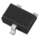
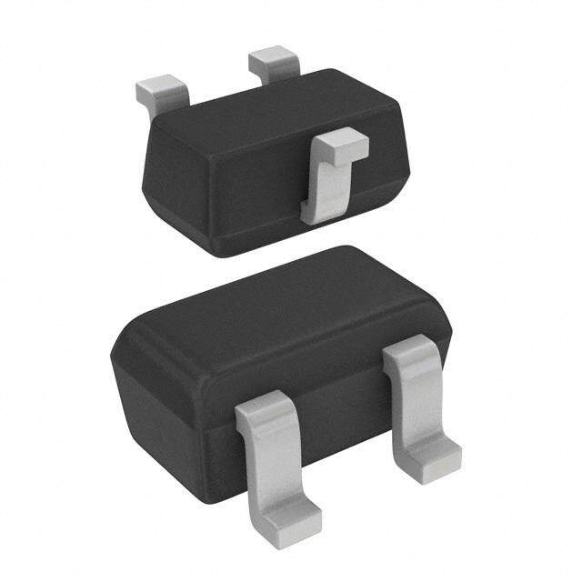
| 产品图片 |
|
| rohs | 符合RoHS无铅 / 符合限制有害物质指令(RoHS)规范要求 |
| 产品系列 | 晶体管,两极晶体管 - BJT,ROHM Semiconductor BC848BWT106- |
| 数据手册 | |
| 产品型号 | BC848BWT106 |
| 不同 Ib、Ic时的 Vce饱和值(最大值) | 600mV @ 5mA,100mA |
| 不同 Ic、Vce 时的DC电流增益(hFE)(最小值) | 200 @ 2mA,5V |
| 产品种类 | 两极晶体管 - BJT |
| 供应商器件封装 | UMT3 |
| 其它名称 | BC848BWT106CT |
| 功率-最大值 | 200mW |
| 包装 | 剪切带 (CT) |
| 发射极-基极电压VEBO | 5 V |
| 商标 | ROHM Semiconductor |
| 增益带宽产品fT | 200 MHz |
| 安装类型 | 表面贴装 |
| 安装风格 | SMD/SMT |
| 封装 | Reel |
| 封装/外壳 | SC-70,SOT-323 |
| 封装/箱体 | SOT-323 |
| 工厂包装数量 | 3000 |
| 晶体管极性 | NPN |
| 晶体管类型 | NPN |
| 最大功率耗散 | 0.2 W |
| 最大工作温度 | + 150 C |
| 最大直流电集电极电流 | 0.1 A |
| 最小工作温度 | - 65 C |
| 标准包装 | 1 |
| 电压-集射极击穿(最大值) | 30V |
| 电流-集电极(Ic)(最大值) | 100mA |
| 电流-集电极截止(最大值) | 100nA(ICBO) |
| 直流电流增益hFE最大值 | 450 |
| 直流集电极/BaseGainhfeMin | 200 |
| 配置 | Single |
| 集电极—发射极最大电压VCEO | 30 V |
| 集电极—基极电压VCBO | 30 V |
| 集电极—射极饱和电压 | 0.6 V |
| 集电极连续电流 | 0.1 A |
| 频率-跃迁 | 200MHz |


PDF Datasheet 数据手册内容提取
BC848BW / BC848B Transistors NPN General Purpose Transistor BC848BW / BC848B (cid:122)Features (cid:122)External dimensions (Unit : mm) 1) BVCEO minimum is 30V (IC=1mA) BC848BW 2) Complements the BC858B / BC858BW. 2.0±0.2 1.3±0.1 0.9±0.1 0.650.65 0.2 0.7±0.1 (1) (2) (3) ±0.11.25 ±2.10.1 0~0.1 ROHM : UMT3 All ter0m.3in+−a00ls.1 have same di0m.1e5n±s0io.0n5s 0.1~0.4 ((12)) EBmasiteter EIAJ : SC-70 (3) Collector BC848B, BC848C 21..99±±00..22 0.95+−00..21 0.950.95 0.45±0.1 (1) (2) (3) +0.21.3−0.1 ±2.40.2 00~.20M.1in. All term0.i4na+−l00s.. 10h5ave same d0im.1e5n−+s00io..01n6s ((12)) EBmasiteter ROHM : SST3 (3) Collector (cid:122)Absolute maximum ratings (Ta=25°C) Parameter Symbol Limits Unit Collector-base voltage VCBO 30 V Collector-emitter voltage VCEO 30 V Emitter-base voltage VEBO 5 V Collector current IC 0.1 A 0.2 W Collector power BC848BW dissipation BC848B PC 00..325 WW ∗ Junction temperature Tj 150 °C Storage temperature Tstg −65~+150 °C ∗ When mounted on a 7×5×0.6mm ceramic board. (cid:122)Electrical characteristics (Ta=25°C) Parameter Symbol Min. Typ. Max. Unit Conditions Collector-base breakdown voltage BVCBO 30 − − V IC=50µA Collector-emitter breakdown voltage BVCEO 30 − − V IC=1mA Emitter-base breakdown voltage BVEBO 5 − − V IE=50µA − − 100 nA VCB=30V Collector cutoff current ICBO − − 5 µA VCB=30V, Ta=150°C − − 0.25 IC/IB=10mA/0.5mA Collector-emitter saturation voltage VCE(sat) − − 0.6 V IC/IB=100mA/5mA Base-emitter saturation voltage VBE(on) 0.58 − 0.77 V VCE/IC=5V/10mA DC current transfer ratio hFE 200 − 450 − VCE/IC=5V/2mA Transition frequency fT − 200 − MHz VCE=5V, IE=−20mA, f=100MHz Collector output capacitance Cob − 3 − pF VCB=10V, IE=0, f=1MHz Collector output capacitance Cib − 8 − pF VEB=0.5V, IE=0, f=1MHz (SPEC-C22) Rev.A 1/5
BC848BW / BC848B Transistors (cid:122)Packaging specifications Part No. BC848BW BC848B Packaging type UMT3 SST3 Marking G1K G1K Code T106 T116 Basic ordering unit (pieces) 3000 3000 (cid:122)Electrical characteristic curves 100 Ta=25°C 1.2 10.0 35 NT (mA)80 001...860 NT (mA)8.0 2350 URRE60 0.4 URRE6.0 20 C C CTOR 40 0.2 CTOR 4.0 15 COLLE20 0.1 COLLE2.0 10 −IC I-C 5 00 1.0 IB=0mA 2.0 00 1.0 IB=0µA Ta=25°C2.0 VCE−COLLECTOR-EMITTER VOLTAGE (V) VCE-COLLECTOR-EMITTER VOLTAGE (V) Fig.1 Grounded emitter output Fig.2 Grounded emitter output characteristics ( ) characteristics ( ) 1000 Ta=25°C N GAI VCE=10V T N RRE100 1V 5V U C C D h-FE 10 0.1 1.0 10 100 1000 IC-COLLECTOR CURRENT (mA) Fig.3 DC current gain vs. collector current ( ) 1000 VCE=5V AIN Ta=125°C G T Ta=25°C EN Ta=−55°C RR100 U C C D h-FE 10 0.1 1.0 10 100 1000 IC-COLLECTOR CURRENT (mA) Fig.4 DC current gain vs. collector current ( ) Rev.A 2/5
BC848BW / BC848B Transistors 1000 Ta=25°C VCE=5V f=1kHz N AI G T N E RR100 U C C A h-FE 10 0.01 0.1 1 10 100 IC-COLLECTOR CURRENT (mA) Fig.5 AC current gain vs. collector current VCOLLECTOR EMITTER SATURATION VOLTAGE (V)CE(SAT) 00000.....F011100886240ig.1.6 CIvC-ooCllOtleaLcgL1tEe.o0C rvT-sOe.Rm c ioCttlUeleRrc R1st0EoaNrtTu c r(TIumCaa/rIAt=Bri=2)oe15nn0°1C t00 VBASE EMITTER SATURATION VOLTAGE (V)BE(SAT)01110F.....828640i0g.1.7 BvICoa-ClstOaeLg-Le1eE.m 0CvTistOt.e Rcr o CsllaUeRtcuR1tro0EarNt iTco u(TInmCra/IrA=Be=2)n150°t1C00 VBASE EMITTER VOLTAGE (V)FBE(ON)i01110g.....828640.08.1 cGhraIoCr-uCanOcdLteeL1Erd.0iCs eTtiOmcRsi t tCeUrR pR1r0EoNpTa (gTVmCaaAE=t=)2i5o5Vn°1C00 1000 Ta=25°C 1000 Ta=25°C 1000 40V Ta=25°C IC/IB=10 IC/IB=10 IC=101B1=101B2 3V t-TURN ON TIME (ns)on100 t-RISE TIME (ns)r100 VCC=40V t-STORAGE TIME (ns)S100 VCE=15V 10 10 10 1.0 10 100 1.0 10 100 1.0 10 100 IC-COLLECTOR CURRENT (mA) IC-COLLECTOR CURRENT (mA) IC-COLLECTOR CURRENT (mA) Fig.9 Turn-on time vs. collector Fig.10 Rise time vs. collector Fig.11 Storage time vs. collector current current current Rev.A 3/5
BC848BW / BC848B Transistors 1000 TVICCa=C=1=204510B°V1C=101B2 100 Tf=a1=M2H5°zC GE (V)50100MHz200MHz300MHz 400MHz Ta=25°C A T t-FALL TIME (ns)f100 CAPACITANCE (pF)10 Cib Cob ECTOR-EMITTER VOL5.0 432100000000MMMMHHHHzzzz L L O C 10 1 V CE0.5 1.0 10 100 0.5 1 10 50 0.5 10 100 500 IC-COLLECTOR CURRENT (mA) REVERSE BIAS VOLTAGE (V) IC-COLLECTOR CURRENT (mA) Fig.12 Fall time vs. collector Fig.13 Input/output capacitance Fig.14 Gain bandwidth product current vs. voltage DUCT (MHz)1000 TVaCE==255V°C D TO 1mA100 hoe TVf=aC2E=7=2065HV°zC URRENT (A) 101nn VCB=30V CURRENT GAIN-BANDWIDTH PRO10100 h PARAMETER NORMALIZE01.011 hrhehofeehie hiehhhhIhhCfrifroe=eeeee1====m7247.8.A8.505k×µΩ1S0−5 I-COLLECTOR CUTOFF CCBO1001.0011PPPP 0.51.0 10 100 500 0.1 1 10 100 0 25 50 75 100 125 150 IC-COLLECTOR CURRENT (mA) IC-COLLECTOR CURRENT (mA) TA-AMBIENT TEMPERATURE (°C) Fig.15 Gain bandwidth product Fig.16 h parameter Fig.17 Collector cutoff current vs. collector current vs. collector current 12 Ta=25°C 100k Ta=25°C E (dB)108 RVICCS=E=1=10500VkµΩA ΩANCE ()10k NF=1dB3dB5dB8dB12dB Vf=C1E0=H5Vz R T U S G SI NOISE FI 64 URCE RE 1k NF 2 R-SOS 0 100 10 100 1k 10k 100k 0.01 0.1 1 10 f-FREQUENCY (Hz) IC-COLLECTOR CURRENT (mA) Fig.18 Noise vs. collector current Fig.19 Noise characteristics ( ) Rev.A 4/5
BC848BW / BC848B Transistors 100k Ta=25°C 100k 100k ΩRESISTANCE ()10k NF=1dB3dB5dB8dB12dB Vf=C3E0=H5Vz ΩRESISTANCE ()10k fTV=aC1E=k=2H55zV°C NF=1dB3dB5dB8dB 12dB ΩRESISTANCE ()10k TVf=aC1E=0=2k55HV°zC NF=1dB 3dB 5dB8dB CE CE CE UR 1k UR 1k UR 1k O O O R-SS R-SS R-SS 100 100 100 0.01 0.1 1 10 0.01 0.1 1 10 0.01 0.1 1 10 IC-COLLECTOR CURRENT (mA) IC-COLLECTOR CURRENT (mA) IC-COLLECTOR CURRENT (mA) Fig.20 Noise characteristics ( ) Fig.21 Noise characteristics ( ) Fig.22 Noise characteristics ( ) Rev.A 5/5
Appendix Notes No technical content pages of this document may be reproduced in any form or transmitted by any means without prior permission of ROHM CO.,LTD. The contents described herein are subject to change without notice. The specifications for the product described in this document are for reference only. Upon actual use, therefore, please request that specifications to be separately delivered. Application circuit diagrams and circuit constants contained herein are shown as examples of standard use and operation. Please pay careful attention to the peripheral conditions when designing circuits and deciding upon circuit constants in the set. Any data, including, but not limited to application circuit diagrams information, described herein are intended only as illustrations of such devices and not as the specifications for such devices. ROHM CO.,LTD. disclaims any warranty that any use of such devices shall be free from infringement of any third party's intellectual property rights or other proprietary rights, and further, assumes no liability of whatsoever nature in the event of any such infringement, or arising from or connected with or related to the use of such devices. Upon the sale of any such devices, other than for buyer's right to use such devices itself, resell or otherwise dispose of the same, no express or implied right or license to practice or commercially exploit any intellectual property rights or other proprietary rights owned or controlled by ROHM CO., LTD. is granted to any such buyer. Products listed in this document are no antiradiation design. The products listed in this document are designed to be used with ordinary electronic equipment or devices (such as audio visual equipment, office-automation equipment, communications devices, electrical appliances and electronic toys). Should you intend to use these products with equipment or devices which require an extremely high level of reliability and the malfunction of with would directly endanger human life (such as medical instruments, transportation equipment, aerospace machinery, nuclear-reactor controllers, fuel controllers and other safety devices), please be sure to consult with our sales representative in advance. About Export Control Order in Japan Products described herein are the objects of controlled goods in Annex 1 (Item 16) of Export Trade Control Order in Japan. In case of export from Japan, please confirm if it applies to "objective" criteria or an "informed" (by MITI clause) on the basis of "catch all controls for Non-Proliferation of Weapons of Mass Destruction. Appendix1-Rev1.1