ICGOO在线商城 > 分立半导体产品 > 晶体管 - 双极 (BJT) - 单 > BC807-40W,115
 Datasheet下载
- 型号: BC807-40W,115
- 制造商: NXP Semiconductors
- 库位|库存: xxxx|xxxx
- 要求:
| 数量阶梯 | 香港交货 | 国内含税 |
| +xxxx | $xxxx | ¥xxxx |
查看当月历史价格
查看今年历史价格
BC807-40W,115产品简介:
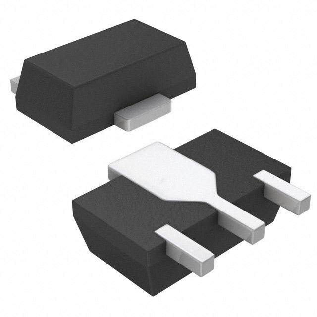
ICGOO电子元器件商城为您提供BC807-40W,115由NXP Semiconductors设计生产,在icgoo商城现货销售,并且可以通过原厂、代理商等渠道进行代购。 BC807-40W,115价格参考。NXP SemiconductorsBC807-40W,115封装/规格:晶体管 - 双极 (BJT) - 单, Bipolar (BJT) Transistor PNP 45V 500mA 80MHz 200mW Surface Mount SC-70。您可以下载BC807-40W,115参考资料、Datasheet数据手册功能说明书,资料中有BC807-40W,115 详细功能的应用电路图电压和使用方法及教程。
Nexperia USA Inc. 的 BC807-40W,115 是一款通用型 PNP 双极结型晶体管(BJT),广泛应用于各类电子电路中。其主要应用场景包括信号放大、开关控制和电源管理等。

在消费类电子产品中,该器件常用于音频信号放大电路或作为小功率开关,控制LED、继电器或电机等负载。由于其较高的直流电流增益(hFE)和良好的开关特性,BC807-40W 特别适用于需要稳定可靠开关动作的场合,如家用电器控制板、遥控器和智能设备中的驱动电路。

在工业控制领域,该晶体管可用于传感器信号调理、逻辑电平转换和继电器驱动等应用。其SOT-23封装体积小巧,适合高密度贴装的印刷电路板,有利于实现设备小型化。

此外,BC807-40W,115 还常与 NPN 型晶体管(如 BC817)配对使用,构成互补推挽输出级,广泛应用于功率输出级或驱动桥式电路。

总体而言,该型号因其高可靠性、良好温度特性和成本优势,被广泛用于汽车电子、便携式设备、电源模块及各类嵌入式系统中,是一款性能稳定的通用型晶体管。
| 参数 | 数值 |
| 产品目录 | |
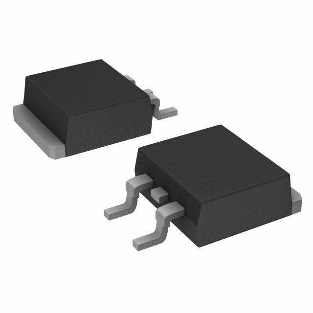
| 描述 | TRANSISTOR PNP 500MA 45V SOT323两极晶体管 - BJT TRANS GP TAPE-7 |
| 产品分类 | 晶体管(BJT) - 单路分离式半导体 |
| 品牌 | NXP Semiconductors |
| 产品手册 | |
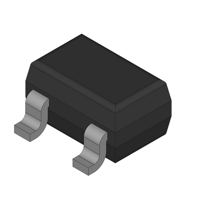
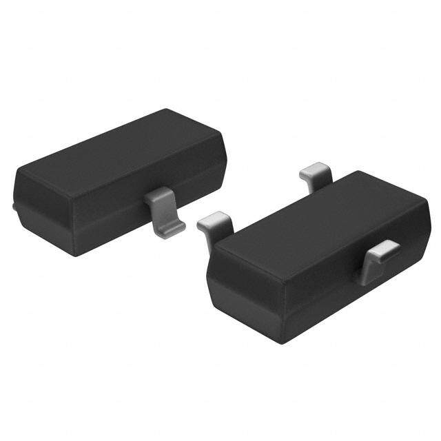
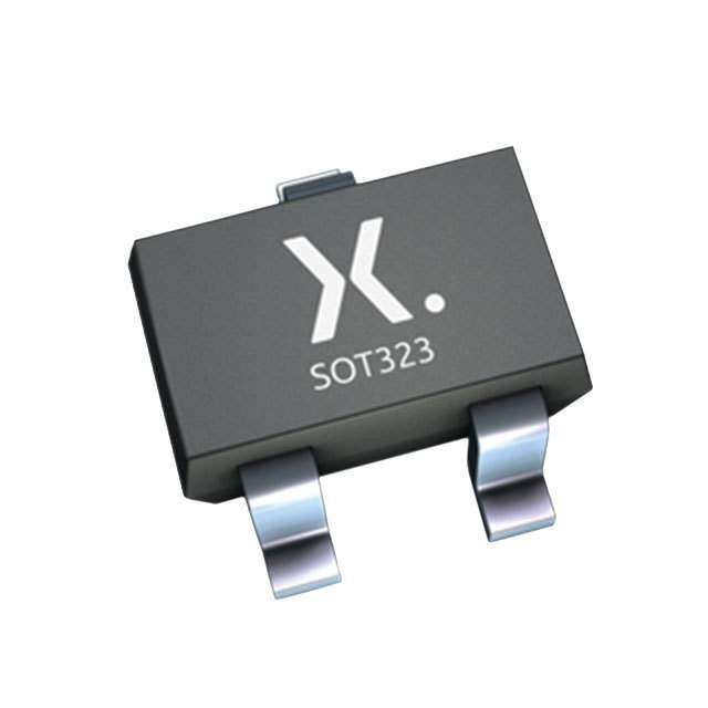
| 产品图片 |
|
| rohs | 符合RoHS无铅 / 符合限制有害物质指令(RoHS)规范要求 |
| 产品系列 | 晶体管,两极晶体管 - BJT,NXP Semiconductors BC807-40W,115- |
| 数据手册 | |
| 产品型号 | BC807-40W,115 |
| PCN封装 | |
| PCN设计/规格 | |
| 不同 Ib、Ic时的 Vce饱和值(最大值) | 700mV @ 50mA,500mA |
| 不同 Ic、Vce 时的DC电流增益(hFE)(最小值) | 250 @ 100mA,1V |
| 产品种类 | 两极晶体管 - BJT |
| 供应商器件封装 | SOT-323 |
| 其它名称 | 568-6049-6 |
| 功率-最大值 | 200mW |
| 包装 | Digi-Reel® |
| 发射极-基极电压VEBO | 5 V |
| 商标 | NXP Semiconductors |
| 增益带宽产品fT | 80 MHz |
| 安装类型 | 表面贴装 |
| 安装风格 | SMD/SMT |
| 封装 | Reel |
| 封装/外壳 | SC-70,SOT-323 |
| 封装/箱体 | SOT-323 |
| 工厂包装数量 | 3000 |
| 晶体管极性 | PNP |
| 晶体管类型 | PNP |
| 最大功率耗散 | 200 mW |
| 最大工作温度 | + 150 C |
| 最大直流电集电极电流 | 0.5 A |
| 最小工作温度 | - 65 C |
| 标准包装 | 1 |
| 特色产品 | http://www.digikey.com/cn/zh/ph/NXP/I2C.html |
| 电压-集射极击穿(最大值) | 45V |
| 电流-集电极(Ic)(最大值) | 500mA |
| 电流-集电极截止(最大值) | - |
| 直流电流增益hFE最大值 | 250 at 100 mA at 1 V |
| 配置 | Single |
| 集电极—发射极最大电压VCEO | 45 V |
| 集电极—基极电压VCBO | 50 V |
| 零件号别名 | BC807-40W T/R |
| 频率-跃迁 | 80MHz |


PDF Datasheet 数据手册内容提取
BC807; BC807W; BC327 45 V, 500 mA PNP general-purpose transistors Rev. 06 — 17 November 2009 Product data sheet 1. Product profile 1.1 General description PNP general-purpose transistors. Table 1. Product overview Type number Package NPN complement NXP JEITA BC807 SOT23 - BC817 BC807W SOT323 SC-70 BC817W BC327[1] SOT54 (TO-92) SC-43A BC337 [1] Also available in SOT54A and SOT54 variant packages (see Section2). 1.2 Features (cid:132) High current (cid:132) Low voltage 1.3 Applications (cid:132) General-purpose switching and amplification 1.4 Quick reference data Table 2. Quick reference data Symbol Parameter Conditions Min Typ Max Unit V collector-emitter voltage open base; - - −45 V CEO I =10mA C I collector current (DC) - - −500 mA C I peak collector current - - −1 A CM h DC current gain I = −100 mA; [1] FE C V =−1V CE BC807; BC807W; BC327 100 - 600 BC807-16; BC807-16W; BC327-16 100 - 250 BC807-25; BC807-25W; BC327-25 160 - 400 BC807-40; BC807-40W; BC327-40 250 - 600 [1] Pulse test: tp ≤ 300 μs; δ ≤ 0.02.
BC807; BC807W; BC327 NXP Semiconductors 45 V, 500 mA PNP general-purpose transistors 2. Pinning information Table 3. Pinning Pin Description Simplified outline Symbol SOT23 1 base 3 3 2 emitter 3 collector 1 1 2 2 sym013 SOT323 1 base 3 3 2 emitter 3 collector 1 2 sym013 1 2 sot323_so SOT54 1 emitter 3 2 base 3 collector 1 2 2 3 1 001aab347 006aaa149 SOT54A 1 emitter 3 2 base 3 collector 1 2 2 3 1 001aab348 006aaa149 SOT54 variant 1 emitter 3 2 base 3 collector 1 2 2 3 1 001aab447 006aaa149 BC807_BC807W_BC327_6 © NXP B.V. 2009. All rights reserved. Product data sheet Rev. 06 — 17 November 2009 2 of 19
BC807; BC807W; BC327 NXP Semiconductors 45 V, 500 mA PNP general-purpose transistors 3. Ordering information Table 4. Ordering information Type number[1] Package Name Description Version BC807 - plastic surface mounted package; 3 leads SOT23 BC807W SC-70 plastic surface mounted package; 3 leads SOT323 BC327[2] SC-43A plastic single-ended leaded (through hole) package; SOT54 3leads [1] Valid for all available selection groups. [2] Also available in SOT54A and SOT54 variant packages (see Section2 and Section9). 4. Marking Table 5. Marking codes Type number Marking code[1] BC807 5D* BC807-16 5A* BC807-25 5B* BC807-40 5C* BC807W 5D* BC807-16W 5A* BC807-25W 5B* BC807-40W 5C* BC327 C327 BC327-16 C32716 BC327-25 C32725 BC327-40 C32740 [1] * = -: made in Hong Kong * = p: made in Hong Kong * = t: made in Malaysia * = W: made in China BC807_BC807W_BC327_6 © NXP B.V. 2009. All rights reserved. Product data sheet Rev. 06 — 17 November 2009 3 of 19
BC807; BC807W; BC327 NXP Semiconductors 45 V, 500 mA PNP general-purpose transistors 5. Limiting values Table 6. Limiting values In accordance with the Absolute Maximum Rating System (IEC 60134). Symbol Parameter Conditions Min Max Unit V collector-base voltage open emitter - −50 V CBO V collector-emitter voltage open base; - −45 V CEO I =10mA C V emitter-base voltage open collector - −5 V EBO I collector current (DC) - −500 mA C I peak collector current - −1 A CM I peak base current - −200 mA BM P total power dissipation tot BC807 T ≤ 25 °C [1][2] - 250 mW amb BC807W T ≤ 25 °C [1][2] - 200 mW amb BC327 T ≤ 25 °C [1][2] - 625 mW amb T storage temperature −65 +150 °C stg T junction temperature - 150 °C j T ambient temperature −65 +150 °C amb [1] Transistor mounted on an FR4 printed-circuit board, single-sided copper, tin-plated and standard footprint. [2] Valid for all available selection groups. 6. Thermal characteristics Table 7. Thermal characteristics Symbol Parameter Conditions Min Typ Max Unit R thermal resistance from th(j-a) junction to ambient BC807 T ≤ 25 °C [1][2] - - 500 K/W amb BC807W T ≤ 25 °C [1][2] - - 625 K/W amb BC327 T ≤ 25 °C [1][2] - - 200 K/W amb [1] Transistor mounted on an FR4 printed-circuit board, single-sided copper, tin-plated and standard footprint. [2] Valid for all available selection groups. BC807_BC807W_BC327_6 © NXP B.V. 2009. All rights reserved. Product data sheet Rev. 06 — 17 November 2009 4 of 19
BC807; BC807W; BC327 NXP Semiconductors 45 V, 500 mA PNP general-purpose transistors 7. Characteristics Table 8. Characterist ics T = 25 °C unless otherwise specified. amb Symbol Parameter Conditions Min Typ Max Unit I collector-base cut-off current I = 0 A; V = −20 V - - −100 nA CBO E CB I = 0 A; V = −20 V; - - −5 μA E CB T =150°C j I emitter-base cut-off current I = 0 A; V = −5 V - - −100 nA EBO C EB h DC current gain I = −100 mA; V = −1 V [1] FE C CE BC807; BC807W; BC327 100 - 600 BC807-16; BC807-16W; 100 - 250 BC327-16 BC807-25; BC807-25W; 160 - 400 BC327-25 BC807-40; BC807-40W; 250 - 600 BC327-40 h DC current gain I = −500 mA; V = −1 V [1] 40 - - FE C CE V collector-emitter saturation I = −500 mA; I = −50 mA [1] - - −700 mV CEsat C B voltage V base-emitter voltage I = −500 mA; V = −1 V [2] - - −1.2 V BE C CE C collector capacitance I = i = 0 A; V = −10 V; - 5 - pF c E e CB f=1MHz f transition frequency I = −10 mA; V = −5 V; 80 - - MHz T C CE f=100MHz [1] Pulse test: tp ≤ 300 μs; δ ≤ 0.02. [2] V decreases by approximately 2 mV/K with increasing temperature. BE BC807_BC807W_BC327_6 © NXP B.V. 2009. All rights reserved. Product data sheet Rev. 06 — 17 November 2009 5 of 19
BC807; BC807W; BC327 NXP Semiconductors 45 V, 500 mA PNP general-purpose transistors 006aaa119 006aaa120 300 600 (1) hFE hFE (1) 200 400 (2) (2) 100 200 (3) (3) 0 0 −10−1 −1 −10 −102 −103 −10−1 −1 −10 −102 −103 IC (mA) IC (mA) VCE = −1 V VCE = −1 V (1) Tamb = 150 °C (1) Tamb = 150 °C (2) Tamb = 25 °C (2) Tamb = 25 °C (3) Tamb = −55 °C (3) Tamb = −55 °C Fig 1. Selection -16: DC current gain as a function of Fig 2. Selection -25: DC current gain as a function of collector current; typical values collector current; typical values 006aaa121 800 hFE 600 (1) 400 (2) 200 (3) 0 −10−1 −1 −10 −102 −103 IC (mA) VCE = −1 V (1) Tamb = 150 °C (2) Tamb = 25 °C (3) Tamb = −55 °C Fig 3. Selection -40: DC current gain as a function of collector current; typical values BC807_BC807W_BC327_6 © NXP B.V. 2009. All rights reserved. Product data sheet Rev. 06 — 17 November 2009 6 of 19
BC807; BC807W; BC327 NXP Semiconductors 45 V, 500 mA PNP general-purpose transistors −10 006aaa122 −10 006aaa123 VBEsat VBEsat (V) (V) −1 (1) −1 (1) (2) (2) (3) (3) −10−1 −10−1 −10−1 −1 −10 −102 −103 −10−1 −1 −10 −102 −103 IC (mA) IC (mA) I /I = 10 I /I = 10 C B C B (1) Tamb = −55 °C (1) Tamb = −55 °C (2) Tamb = 25 °C (2) Tamb = 25 °C (3) Tamb = 150 °C (3) Tamb = 150 °C Fig 4. Selection -16: Base-emitter saturation voltage Fig 5. Selection -25: Base-emitter saturation voltage as a function of collector current; typical as a function of collector current; typical values values −10 006aaa124 VBEsat (V) −1 (1) (2) (3) −10−1 −10−1 −1 −10 −102 −103 IC (mA) I /I = 10 C B (1) Tamb = −55 °C (2) Tamb = 25 °C (3) Tamb = 150 °C Fig 6. Selection -40: Base-emitter saturation voltage as a function of collector current; typical values BC807_BC807W_BC327_6 © NXP B.V. 2009. All rights reserved. Product data sheet Rev. 06 — 17 November 2009 7 of 19
BC807; BC807W; BC327 NXP Semiconductors 45 V, 500 mA PNP general-purpose transistors −1 006aaa125 −1 006aaa126 VCEsat VCEsat (V) (V) −10−1 −10−1 (1) (2) −10−2 (3) (1) (2) (3) −10−2 −10−3 −10−1 −1 −10 −102 −103 −10−1 −1 −10 −102 −103 IC (mA) IC (mA) I /I = 10 I /I = 10 C B C B (1) Tamb = 150 °C (1) Tamb = 150 °C (2) Tamb = 25 °C (2) Tamb = 25 °C (3) Tamb = −55 °C (3) Tamb = −55 °C Fig 7. Selection -16: Collector-emitter saturation Fig 8. Selection- 25: Collector-emitter saturation voltage as a function of collector current; voltage as a function of collector current; typical values typical values −1 006aaa127 VCEsat (V) −10−1 (1) (2) −10−2 (3) −10−3 −10−1 −1 −10 −102 −103 IC (mA) I /I = 10 C B (1) Tamb = 150 °C (2) Tamb = 25 °C (3) Tamb = −55 °C Fig 9. Selection -40: Collector-emitter saturation voltage as a function of collector current; typical values BC807_BC807W_BC327_6 © NXP B.V. 2009. All rights reserved. Product data sheet Rev. 06 — 17 November 2009 8 of 19
BC807; BC807W; BC327 NXP Semiconductors 45 V, 500 mA PNP general-purpose transistors −1.2 006aaa128 −1.2 006aaa129 (3) (2) (1) IC (3) (2) (1) IC (A) (A) (4) (5) (4) −0.8 (5) −0.8 (6) (6) (7) (7) (8) (8) (9) −0.4 (9) −0.4 (10) (10) 0 0 0 −1 −2 −3 −4 −5 0 −1 −2 −3 −4 −5 VCE (V) VCE (V) Tamb = 25 °C Tamb = 25 °C (1) IB = −16.0 mA (1) IB = −13.0 mA (2) IB = −14.4 mA (2) IB = −11.7 mA (3) IB = −12.8 mA (3) IB = −10.4 mA (4) IB = −11.2 mA (4) IB = −9.1 mA (5) IB = −9.6 mA (5) IB = −7.8 mA (6) IB = −8.0 mA (6) IB = −6.5 mA (7) IB = −6.4 mA (7) IB = −5.2 mA (8) IB = −4.8 mA (8) IB = −3.9 mA (9) IB = −3.2 mA (9) IB = −2.6 mA (10) IB = −1.6 mA (10) IB = −1.3 mA Fig 10. Selection -16: Collector current as a function Fig 11. Selection -25: Collector current as a function of collector-emitter voltage; typical values of collector-emitter voltage; typical values BC807_BC807W_BC327_6 © NXP B.V. 2009. All rights reserved. Product data sheet Rev. 06 — 17 November 2009 9 of 19
BC807; BC807W; BC327 NXP Semiconductors 45 V, 500 mA PNP general-purpose transistors −1.2 006aaa130 IC (5) (4) (3) (2) (1) (A) −0.8 (6) (7) (8) (9) −0.4 (10) 0 0 −1 −2 −3 −4 −5 VCE (V) Tamb = 25 °C (1) IB = −12.0 mA (2) IB = −10.8 mA (3) IB = −9.6 mA (4) IB = −8.4 mA (5) IB = −7.2 mA (6) IB = −6.0 mA (7) IB = −4.8 mA (8) IB = −3.6 mA (9) IB = −2.4 mA (10) IB = −1.2 mA Fig 12. Selection -40: Collector current as a function of collector-emitter voltage; typical values BC807_BC807W_BC327_6 © NXP B.V. 2009. All rights reserved. Product data sheet Rev. 06 — 17 November 2009 10 of 19
BC807; BC807W; BC327 NXP Semiconductors 45 V, 500 mA PNP general-purpose transistors 8. Package outline Plastic surface-mounted package; 3 leads SOT23 D B E A X HE v M A 3 Q A A1 1 2 c e1 bp w M B Lp e detail X 0 1 2 mm scale DIMENSIONS (mm are the original dimensions) UNIT A mAa1x. bp c D E e e1 HE Lp Q v w 1.1 0.48 0.15 3.0 1.4 2.5 0.45 0.55 mm 0.1 1.9 0.95 0.2 0.1 0.9 0.38 0.09 2.8 1.2 2.1 0.15 0.45 OUTLINE REFERENCES EUROPEAN ISSUE DATE VERSION IEC JEDEC JEITA PROJECTION 04-11-04 SOT23 TO-236AB 06-03-16 Fig 13. Package outline SOT23 (TO-236AB) BC807_BC807W_BC327_6 © NXP B.V. 2009. All rights reserved. Product data sheet Rev. 06 — 17 November 2009 11 of 19
BC807; BC807W; BC327 NXP Semiconductors 45 V, 500 mA PNP general-purpose transistors Plastic surface-mounted package; 3 leads SOT323 D B E A X y HE v M A 3 Q A A1 c 1 2 e1 bp w M B Lp e detail X 0 1 2 mm scale DIMENSIONS (mm are the original dimensions) UNIT A mAa1x bp c D E e e1 HE Lp Q v w 1.1 0.4 0.25 2.2 1.35 2.2 0.45 0.23 mm 0.1 1.3 0.65 0.2 0.2 0.8 0.3 0.10 1.8 1.15 2.0 0.15 0.13 OUTLINE REFERENCES EUROPEAN ISSUE DATE VERSION IEC JEDEC JEITA PROJECTION 04-11-04 SOT323 SC-70 06-03-16 Fig 14. Package outline SOT323 (SC-70) BC807_BC807W_BC327_6 © NXP B.V. 2009. All rights reserved. Product data sheet Rev. 06 — 17 November 2009 12 of 19
BC807; BC807W; BC327 NXP Semiconductors 45 V, 500 mA PNP general-purpose transistors Plastic single-ended leaded (through hole) package; 3 leads SOT54 c E d A L b 1 e1 2 D e 3 b1 L1 0 2.5 5 mm scale DIMENSIONS (mm are the original dimensions) UNIT A b b1 c D d E e e1 L Lm1a(x1.) 5.2 0.48 0.66 0.45 4.8 1.7 4.2 14.5 mm 2.54 1.27 2.5 5.0 0.40 0.55 0.38 4.4 1.4 3.6 12.7 Note 1. Terminal dimensions within this zone are uncontrolled to allow for flow of plastic and terminal irregularities. OUTLINE REFERENCES EUROPEAN ISSUE DATE VERSION IEC JEDEC JEITA PROJECTION 04-06-28 SOT54 TO-92 SC-43A 04-11-16 Fig 15. Package outline SOT54 (SC-43A/TO-92) BC807_BC807W_BC327_6 © NXP B.V. 2009. All rights reserved. Product data sheet Rev. 06 — 17 November 2009 13 of 19
BC807; BC807W; BC327 NXP Semiconductors 45 V, 500 mA PNP general-purpose transistors Plastic single-ended leaded (through hole) package; 3 leads (wide pitch) SOT54A c E A L d L2 b 1 e1 D e 2 3 b1 L1 0 2.5 5 mm scale DIMENSIONS (mm are the original dimensions) UNIT A b b1 c D d E e e1 L L1(1) L2 max. 5.2 0.48 0.66 0.45 4.8 1.7 4.2 14.5 3 mm 5.08 2.54 3 5.0 0.40 0.55 0.38 4.4 1.4 3.6 12.7 2 Note 1. Terminal dimensions within this zone are uncontrolled to allow for flow of plastic and terminal irregularities. OUTLINE REFERENCES EUROPEAN ISSUE DATE VERSION IEC JEDEC JEITA PROJECTION 97-05-13 SOT54A 04-06-28 Fig 16. Package outline SOT54A BC807_BC807W_BC327_6 © NXP B.V. 2009. All rights reserved. Product data sheet Rev. 06 — 17 November 2009 14 of 19
BC807; BC807W; BC327 NXP Semiconductors 45 V, 500 mA PNP general-purpose transistors Plastic single-ended leaded (through hole) package; 3 leads (on-circle) SOT54 variant c e1 L2 E d A L b 1 2 e1 D e 3 b1 L1 0 2.5 5 mm scale DIMENSIONS (mm are the original dimensions) UNIT A b b1 c D d E e e1 L Lm1a(1x) mLa2x 5.2 0.48 0.66 0.45 4.8 1.7 4.2 14.5 mm 2.54 1.27 2.5 2.5 5.0 0.40 0.55 0.38 4.4 1.4 3.6 12.7 Note 1. Terminal dimensions within this zone are uncontrolled to allow for flow of plastic and terminal irregularities. OUTLINE REFERENCES EUROPEAN ISSUE DATE VERSION IEC JEDEC JEITA PROJECTION 04-06-28 SOT54 variant 05-01-10 Fig 17. Package outline SOT54 variant BC807_BC807W_BC327_6 © NXP B.V. 2009. All rights reserved. Product data sheet Rev. 06 — 17 November 2009 15 of 19
BC807; BC807W; BC327 NXP Semiconductors 45 V, 500 mA PNP general-purpose transistors 9. Packing information Table 9. Packing met hods The indicated -xxx are the last three digits of the 12NC ordering code.[1] Type number Package Description Packing quantity 3000 5000 10000 BC807 SOT23 4 mm pitch, 8 mm tape and reel -215 - -235 BC807W SOT323 4 mm pitch, 8 mm tape and reel -115 - -135 BC327 SOT54 bulk, straight leads - -412 - BC327 SOT54A tape and reel, wide pitch - - -116 BC327 SOT54A tape ammopack, wide pitch - - -126 BC327 SOT 54 variant bulk, delta pinning (on-circle) - -112 - [1] For further information and the availability of packing methods, see Section12. BC807_BC807W_BC327_6 © NXP B.V. 2009. All rights reserved. Product data sheet Rev. 06 — 17 November 2009 16 of 19
BC807; BC807W; BC327 NXP Semiconductors 45 V, 500 mA PNP general-purpose transistors 10. Revision history Table 10. Revision history Document ID Release date Data sheet status Change notice Supersedes BC807_BC807W_ 20091117 Product data sheet - BC807_BC807W_ BC327_6 BC327_5 Modifications: • This data sheet was changed to reflect the new company name NXP Semiconductors, including new legal definitions and disclaimers. No changes were made to the technical content. • Table 3 “Pinning”: updated • Figure 13 “Package outline SOT23 (TO-236AB)”: updated • Figure 14 “Package outline SOT323 (SC-70)”: updated BC807_BC807W_ 20050221 Product data sheet CPCN200302007F BC807_4; BC807W_3; BC327_5 CPCN200405006F BC327_3 BC807_4 20040116 Product specification - BC807_3 BC807W_3 19990518 Product specification - BC807W_808W_CNV_2 BC327_3 19990415 Product specification - BC327_2 BC807_BC807W_BC327_6 © NXP B.V. 2009. All rights reserved. Product data sheet Rev. 06 — 17 November 2009 17 of 19
BC807; BC807W; BC327 NXP Semiconductors 45 V, 500 mA PNP general-purpose transistors 11. Legal information 11.1 Data sheet status Document status[1][2] Product status[3] Definition Objective [short] data sheet Development This document contains data from the objective specification for product development. Preliminary [short] data sheet Qualification This document contains data from the preliminary specification. Product [short] data sheet Production This document contains the product specification. [1] Please consult the most recently issued document before initiating or completing a design. [2] The term ‘short data sheet’ is explained in section “Definitions”. [3] The product status of device(s) described in this document may have changed since this document was published and may differ in case of multiple devices. The latest product status information is available on the Internet at URLhttp://www.nxp.com. 11.2 Definitions damage. NXP Semiconductors accepts no liability for inclusion and/or use of NXP Semiconductors products in such equipment or applications and therefore such inclusion and/or use is at the customer’s own risk. Draft — The document is a draft version only. The content is still under internal review and subject to formal approval, which may result in Applications — Applications that are described herein for any of these modifications or additions. NXP Semiconductors does not give any products are for illustrative purposes only. NXP Semiconductors makes no representations or warranties as to the accuracy or completeness of representation or warranty that such applications will be suitable for the information included herein and shall have no liability for the consequences of specified use without further testing or modification. use of such information. Limiting values — Stress above one or more limiting values (as defined in Short data sheet — A short data sheet is an extract from a full data sheet the Absolute Maximum Ratings System of IEC60134) may cause permanent with the same product type number(s) and title. A short data sheet is intended damage to the device. Limiting values are stress ratings only and operation of for quick reference only and should not be relied upon to contain detailed and the device at these or any other conditions above those given in the full information. For detailed and full information see the relevant full data Characteristics sections of this document is not implied. Exposure to limiting sheet, which is available on request via the local NXP Semiconductors sales values for extended periods may affect device reliability. office. In case of any inconsistency or conflict with the short data sheet, the Terms and conditions of sale — NXP Semiconductors products are sold full data sheet shall prevail. subject to the general terms and conditions of commercial sale, as published at http://www.nxp.com/profile/terms, including those pertaining to warranty, 11.3 Disclaimers intellectual property rights infringement and limitation of liability, unless explicitly otherwise agreed to in writing by NXP Semiconductors. In case of any inconsistency or conflict between information in this document and such General — Information in this document is believed to be accurate and terms and conditions, the latter will prevail. reliable. However, NXP Semiconductors does not give any representations or No offer to sell or license — Nothing in this document may be interpreted or warranties, expressed or implied, as to the accuracy or completeness of such construed as an offer to sell products that is open for acceptance or the grant, information and shall have no liability for the consequences of use of such conveyance or implication of any license under any copyrights, patents or information. other industrial or intellectual property rights. Right to make changes — NXP Semiconductors reserves the right to make Export control — This document as well as the item(s) described herein changes to information published in this document, including without may be subject to export control regulations. Export might require a prior limitation specifications and product descriptions, at any time and without authorization from national authorities. notice. This document supersedes and replaces all information supplied prior to the publication hereof. Quick reference data — The Quick reference data is an extract of the product data given in the Limiting values and Characteristics sections of this Suitability for use — NXP Semiconductors products are not designed, document, and as such is not complete, exhaustive or legally binding. authorized or warranted to be suitable for use in medical, military, aircraft, space or life support equipment, nor in applications where failure or malfunction of an NXP Semiconductors product can reasonably be expected 11.4 Trademarks to result in personal injury, death or severe property or environmental Notice: All referenced brands, product names, service names and trademarks are the property of their respective owners. 12. Contact information For more information, please visit: http://www.nxp.com For sales office addresses, please send an email to: salesaddresses@nxp.com BC807_BC807W_BC327_6 © NXP B.V. 2009. All rights reserved. Product data sheet Rev. 06 — 17 November 2009 18 of 19
BC807; BC807W; BC327 NXP Semiconductors 45 V, 500 mA PNP general-purpose transistors 13. Contents 1 Product profile. . . . . . . . . . . . . . . . . . . . . . . . . . 1 1.1 General description . . . . . . . . . . . . . . . . . . . . . 1 1.2 Features. . . . . . . . . . . . . . . . . . . . . . . . . . . . . . 1 1.3 Applications . . . . . . . . . . . . . . . . . . . . . . . . . . . 1 1.4 Quick reference data . . . . . . . . . . . . . . . . . . . . 1 2 Pinning information. . . . . . . . . . . . . . . . . . . . . . 2 3 Ordering information. . . . . . . . . . . . . . . . . . . . . 3 4 Marking. . . . . . . . . . . . . . . . . . . . . . . . . . . . . . . . 3 5 Limiting values. . . . . . . . . . . . . . . . . . . . . . . . . . 4 6 Thermal characteristics . . . . . . . . . . . . . . . . . . 4 7 Characteristics. . . . . . . . . . . . . . . . . . . . . . . . . . 5 8 Package outline. . . . . . . . . . . . . . . . . . . . . . . . 11 9 Packing information . . . . . . . . . . . . . . . . . . . . 16 10 Revision history. . . . . . . . . . . . . . . . . . . . . . . . 17 11 Legal information. . . . . . . . . . . . . . . . . . . . . . . 18 11.1 Data sheet status . . . . . . . . . . . . . . . . . . . . . . 18 11.2 Definitions. . . . . . . . . . . . . . . . . . . . . . . . . . . . 18 11.3 Disclaimers. . . . . . . . . . . . . . . . . . . . . . . . . . . 18 11.4 Trademarks. . . . . . . . . . . . . . . . . . . . . . . . . . . 18 12 Contact information. . . . . . . . . . . . . . . . . . . . . 18 13 Contents. . . . . . . . . . . . . . . . . . . . . . . . . . . . . . 19 Please be aware that important notices concerning this document and the product(s) described herein, have been included in section ‘Legal information’. © NXP B.V. 2009. All rights reserved. For more information, please visit: http://www.nxp.com For sales office addresses, please send an email to: salesaddresses@nxp.com Date of release: 17 November 2009 Document identifier: BC807_BC807W_BC327_6