ICGOO在线商城 > 射频/IF 和 RFID > RF 检测器 > AD8363ACPZ-R7
 Datasheet下载
- 型号: AD8363ACPZ-R7
- 制造商: Analog
- 库位|库存: xxxx|xxxx
- 要求:
| 数量阶梯 | 香港交货 | 国内含税 |
| +xxxx | $xxxx | ¥xxxx |
查看当月历史价格
查看今年历史价格
AD8363ACPZ-R7产品简介:
ICGOO电子元器件商城为您提供AD8363ACPZ-R7由Analog设计生产,在icgoo商城现货销售,并且可以通过原厂、代理商等渠道进行代购。 AD8363ACPZ-R7价格参考¥33.69-¥33.69。AnalogAD8363ACPZ-R7封装/规格:RF 检测器, RF Detector IC Cellular, GSM, CDMA, W-CDMA 50Hz ~ 6GHz -50dBm ~ 0dBm ±0.5dB 16-VQFN Exposed Pad, CSP。您可以下载AD8363ACPZ-R7参考资料、Datasheet数据手册功能说明书,资料中有AD8363ACPZ-R7 详细功能的应用电路图电压和使用方法及教程。
AD8363ACPZ-R7 是由 Analog Devices Inc.(现为 Analog Devices, Inc. 与 Linear Technology 合并后的一部分)生产的一款 RF 检测器,属于 AD8363 系列。该器件是一款高精度、宽动态范围的对数功率检测器,专为射频 (RF) 和中频 (IF) 应用设计。以下是其主要应用场景:

 1. 无线通信系统
   - 基站和中继器:用于监测和控制发射信号的功率水平,确保信号强度符合规范并避免过载或失真。
   - 移动设备:在手机、Wi-Fi 模块和其他无线终端中,用于功率放大器的输出功率监控,实现高效的功率管理。
   - 软件定义无线电 (SDR):提供精确的功率测量,支持多种调制模式下的信号处理。

 2. 雷达和导航系统
   - 脉冲雷达:用于检测接收信号的强度,帮助确定目标的距离和方向。
   - 卫星通信:监测上行链路和下行链路的功率水平,确保信号传输的稳定性和可靠性。

 3. 测试与测量设备
   - 频谱分析仪:作为核心组件之一,用于测量输入信号的功率电平。
   - 功率计:提供快速、准确的功率读数,适用于实验室和生产环境中的校准与测试。

 4. 工业与医疗设备
   - 工业无线传感器网络 (WSN):用于监控传感器节点的发射功率,优化电池寿命。
   - 医疗成像设备:如超声波设备中,用于控制发射和接收信号的功率水平,以提高图像质量。

 5. 物联网 (IoT) 和智能家居
   - 在低功耗无线模块中,用于实时监测功率以优化能耗。
   - 在 Zigbee、蓝牙和 LoRa 等协议中,确保信号传输的稳定性。

 特性优势
- 宽动态范围:支持高达 60 dB 的输入信号范围,适应多种功率水平的应用。
- 快速响应时间:能够迅速检测信号变化,适合高速应用。
- 高线性度:确保输出电压与输入功率之间的对数关系准确可靠。
- 低功耗:非常适合便携式和电池供电设备。

综上所述,AD8363ACPZ-R7 广泛应用于需要精确功率测量的领域,特别是在无线通信、雷达、测试设备以及 IoT 等场景中表现出色。
| 参数 | 数值 |
| 产品目录 | |
| 描述 | IC DETECTOR RF/IF TRUPWR 16LFCSP |
| 产品分类 | |
| 品牌 | Analog Devices Inc |
| 数据手册 | |
| 产品图片 |
|
| 产品型号 | AD8363ACPZ-R7 |
| PCN其它 | |
| PCN组件/产地 | |
| RF类型 | 手机,GSM,CDMA,W-CDMA |
| rohs | 无铅 / 符合限制有害物质指令(RoHS)规范要求 |
| 产品系列 | - |
| 产品培训模块 | http://www.digikey.cn/PTM/IndividualPTM.page?site=cn&lang=zhs&ptm=25139 |
| 产品目录页面 | |
| 其它名称 | AD8363ACPZ-R7DKR |
| 包装 | Digi-Reel® |
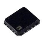
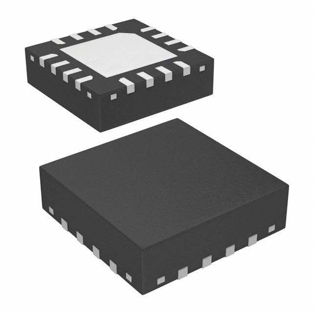
| 封装/外壳 | 16-VQFN 裸露焊盘,CSP |
| 标准包装 | 1 |
| 电压-电源 | 4.5 V ~ 5.5 V |
| 电流-电源 | 60mA |
| 精度 | ±0.5dB |
| 视频文件 | http://www.digikey.cn/classic/video.aspx?PlayerID=1364138032001&width=640&height=505&videoID=2245193150001 |
| 输入范围 | -50dBm ~ 0dBm |
| 频率 | 50Hz ~ 6GHz |


- 商务部:美国ITC正式对集成电路等产品启动337调查
- 曝三星4nm工艺存在良率问题 高通将骁龙8 Gen1或转产台积电
- 太阳诱电将投资9.5亿元在常州建新厂生产MLCC 预计2023年完工
- 英特尔发布欧洲新工厂建设计划 深化IDM 2.0 战略
- 台积电先进制程称霸业界 有大客户加持明年业绩稳了
- 达到5530亿美元!SIA预计今年全球半导体销售额将创下新高
- 英特尔拟将自动驾驶子公司Mobileye上市 估值或超500亿美元
- 三星加码芯片和SET,合并消费电子和移动部门,撤换高东真等 CEO
- 三星电子宣布重大人事变动 还合并消费电子和移动部门
- 海关总署:前11个月进口集成电路产品价值2.52万亿元 增长14.8%


PDF Datasheet 数据手册内容提取
50 Hz to 6 GHz, 50 dB TruPwr™ Detector Data Sheet AD8363 FEATURES FUNCTIONAL BLOCK DIAGRAM Accurate rms-to-dc conversion from 50 Hz to 6 GHz VTGT VREF VPOS COMM 12 11 10 9 Single-ended input dynamic range of >50 dB No balun or external input tuning required NC 13 AD8363 8 TEMP Waveform and modulation independent RF power detection Linear-in-decibels output, scaled: 52 mV/dB Log conformance error: <±0.15 dB X2 INHI 14 7 VSET Temperature stability: <±0.5 dB Voltage supply range: 4.5 V to 5.5 V X2 Operating temperature range: −40°C to +125°C Power-down capability to 1.5 mW INLO 15 6 VOUT Small footprint, 4 mm × 4 mm, LFCSP TCM1 16 5 CLPF APPLICATIONS PMouwltei-rS atmanpdliafriedr, Mlinuelatir-iCzaartrioienr/ Wcoinretlreosls l oInofpras structure TCM2/1PWDN CH2PF VP3OS CO4MM 07368-001 Figure 1. AD8363 Block Diagram (MCGSM, CDMA, WCDMA, TD-SCDMA, WiMAX, LTE) Transmitter power control Transmitter signal strength indication (TSSI) RF instrumentation GENERAL DESCRIPTION The AD8363 is a true rms responding power detector that can Used as a power measurement device, VOUT is connected to be directly driven with a single-ended 50 Ω source. This feature VSET. The output is then proportional to the logarithm of the makes the AD8363 frequency versatile by eliminating the need rms value of the input. The reading is presented directly in for a balun or any other form of external input tuning for operation decibels and is conveniently scaled to 52 mV/dB, or approximately up to 6 GHz. 1 V per decade; however, other slopes are easily arranged. In controller mode, the voltage applied to VSET determines the The AD8363 provides an accurate power measurement, power level required at the input to null the deviation from the independent of waveform, for a variety of high frequency setpoint. The output buffer can provide high load currents. communication and instrumentation systems. Requiring only a single supply of 5 V and a few capacitors, it is easy to use and The AD8363 has 1.5 mW power consumption when powered provides high measurement accuracy. The AD8363 can operate down by a logic high applied to the TCM2/PWDN pin. It powers from arbitrarily low frequencies to 6 GHz and can accept inputs up within about 30 μs to its nominal operating current of 60 mA at that have rms values from less than −50 dBm to at least 0 dBm, 25°C. The AD8363 is available in a 4 mm × 4 mm 16-lead LFCSP with large crest factors exceeding the requirements for accurate for operation over the −40°C to +125°C temperature range. measurement of WiMAX, CDMA, W-CDMA, TD-SCDMA, A fully populated RoHS compliant evaluation board is also multicarrier GSM, and LTE signals. available. The AD8363 can determine the true power of a high frequency signal having a complex low frequency modulation envelope, or it can be used as a simple low frequency rms voltmeter. The high- pass corner generated by its internal offset-nulling loop can be lowered by a capacitor added on the CHPF pin. Rev. B Document Feedback Information furnished by Analog Devices is believed to be accurate and reliable. However, no responsibility is assumed by Analog Devices for its use, nor for any infringements of patents or other One Technology Way, P.O. Box 9106, Norwood, MA 02062-9106, U.S.A. rights of third parties that may result from its use. Specifications subject to change without notice. No license is granted by implication or otherwise under any patent or patent rights of Analog Devices. Tel: 781.329.4700 ©2009–2015 Analog Devices, Inc. All rights reserved. Trademarks and registered trademarks are the property of their respective owners. Technical Support www.analog.com
AD8363 Data Sheet TABLE OF CONTENTS Features .............................................................................................. 1 VSET Interface ............................................................................ 17 Applications ....................................................................................... 1 Output Interface ......................................................................... 17 Functional Block Diagram .............................................................. 1 VTGT Interface .......................................................................... 18 General Description ......................................................................... 1 Measurement Mode Basic Connections.................................. 18 Revision History ............................................................................... 2 System Calibration and Error Calculation .............................. 19 Specifications ..................................................................................... 3 Operation to 125°C .................................................................... 19 Absolute Maximum Ratings ............................................................ 7 Output Voltage Scaling .............................................................. 20 ESD Caution .................................................................................. 7 Offset Compensation, Minimum C , and Maximum C LPF HPF Pin Configuration and Function Descriptions ............................. 8 Capacitance Values ..................................................................... 20 Typical Performance Characteristics ............................................. 9 Choosing a Value for CLPF .......................................................... 21 Theory of Operation ...................................................................... 14 RF Pulse Response and VTGT ................................................. 23 Square Law Detector and Amplitude Target .............................. 14 Controller Mode Basic Connections ....................................... 23 RF Input Interface ...................................................................... 15 Constant Output Power Operation .......................................... 24 Choice of RF Input Pin .............................................................. 15 Description of RF Characterization ......................................... 25 Small Signal Loop Response ..................................................... 15 Evaluation and Characterization Circuit Board Layouts ...... 26 Temperature Sensor Interface ................................................... 16 Assembly Drawings .................................................................... 28 VREF Interface ........................................................................... 16 Outline Dimensions ....................................................................... 29 Temperature Compensation Interface ..................................... 16 Ordering Guide .......................................................................... 29 Power-Down Interface ............................................................... 17 REVISION HISTORY 3/15—Rev. A to Rev. B Changes to Figure 2 and Table 3 ..................................................... 8 Changes to Controller Mode Basic Connections Section ......... 23 Updated Outline Dimensions ....................................................... 29 Changes to the Ordering Guide .................................................... 29 7/11—Rev. 0 to Rev. A Changes to Features Section and Applications Section ............... 1 Added 3-Point Calibration to Table 1 for All MHz ...................... 3 Replaced Typical Performance Characteristics Section; Renumbered Sequentially ................................................................ 9 Changes to Theory of Operation Section .................................... 14 Changes to Temperature Compensation Interface Section ...... 16 Changes to System Calibration and Error Calculation Section and Changes to Figure 44 and Figure 45 ....................... 19 Deleted Basis for Error Calculations Section .............................. 20 Changes to Figure 46 ...................................................................... 20 Deleted Selecting and Increasing Calibration Points to Improve Accuracy over a Reduced Range Section ..................... 22 Deleted Altering the Slope Section .............................................. 23 Added Output Voltage Scaling Section ....................................... 23 5/09—Revision 0: Initial Version Rev. B | Page 2 of 29
Data Sheet AD8363 SPECIFICATIONS V = 5 V, T = 25°C, Z = 50 Ω, single-ended input drive, VOUT connected to VSET, V = 1.4 V, C = 3.9 nF, C = 2.7 nF, error POS A O TGT LPF HPF referred to best-fit line (linear regression) from −20 dBm to −40 dBm, unless otherwise noted. Table 1. Parameter Conditions Min Typ Max Unit OVERALL FUNCTION Maximum Input Frequency 6 GHz RF INPUT INTERFACE INHI (Pin 14), INLO (Pin 15), ac-coupled Input Resistance Single-ended drive 50 Ω Common-Mode DC Voltage 2.6 V 100 MHz TCM1 (Pin 16) = 0.47 V, TCM2 (Pin 1) = 1.0 V, INHI input Output Voltage: High Power In P = −10 dBm 2.47 V IN Output Voltage: Low Power In P = −40 dBm 0.92 V IN ±1.0 dB Dynamic Range CW input, T = 25°C A 3-point calibration at 0 dBm, −10 dBm, and −40 dBm 64 dB Best-fit (linear regression) at −20 dBm and −40 dBm 65 dB Maximum Input Level, ±1.0 dB 9 dBm Minimum Input Level, ±1.0 dB −56 dBm Deviation vs. Temperature Deviation from output at 25°C −40°C < T < +85°C; P = −10 dBm −0.2/+0.3 dB A IN −40°C < T < +85°C; P = −40 dBm −0.5/+0.6 dB A IN Logarithmic Slope 51.7 mV/dB Logarithmic Intercept −58 dBm Deviation from CW Response 13 dB peak-to-rms ratio (W-CDMA), over 40 dB dynamic range <±0.1 dB 12 dB peak-to-rms ratio (WiMAX), over 40 dB dynamic range <±0.1 dB 14.0 dB peak-to-rms ratio (16C CDMA2K), over 40 dB dynamic <±0.1 dB range 256 QAM, CF = 8 dB, over 40 dB dynamic range <±0.1 dB Input Impedance Single-ended drive 49 − j0.09 Ω 900 MHz TCM1 (Pin 16) = 0.5 V, TCM2 (Pin 1) = 1.2 V, INHI input Output Voltage: High Power In P = −15 dBm 2.2 V IN Output Voltage: Low Power In P = −40 dBm 0.91 V IN ±1.0 dB Dynamic Range CW input, T = 25°C A 3-point calibration at 0 dBm, −10 dBm, and −40 dBm 60 dB Best-fit (linear regression) at −20 dBm and −40 dBm 54 dB Maximum Input Level, ±1.0 dB −2 dBm Minimum Input Level, ±1.0 dB −56 dBm Deviation vs. Temperature Deviation from output at 25°C −40°C < T < +85°C; P = −15 dBm +0.6/−0.4 dB A IN −40°C < T < +85°C; P = −40 dBm +0.8/−0.6 dB A IN Logarithmic Slope 51.8 mV/dB Logarithmic Intercept −58 dBm Deviation from CW Response 13 dB peak-to-rms ratio (W-CDMA), over 40 dB dynamic range <±0.1 dB 12 dB peak-to-rms ratio (WiMAX), over 40 dB dynamic range <±0.1 dB 14.0 dB peak-to-rms ratio (16C CDMA2K), over 40 dB dynamic <±0.1 dB range 256 QAM, CF = 8 dB, over 40 dB dynamic range <±0.1 dB Input Impedance Single-ended drive 60 − j3.3 Ω Rev. B | Page 3 of 29
AD8363 Data Sheet Parameter Conditions Min Typ Max Unit 1.9 GHz TCM1 (Pin 16) = 0.52 V, TCM2 (Pin 1) = 0.51 V, INHI input Output Voltage: High Power In P = −15 dBm 2.10 V IN Output Voltage: Low Power In P = −40 dBm 0.8 V IN ±1.0 dB Dynamic Range CW input, T = 25°C A 3-point calibration at 0 dBm, −10 dBm, and −40 dBm 56 dB Best-fit (linear regression) at −20 dBm and −40 dBm 48 dB Maximum Input Level, ±1.0 dB −6 dBm Minimum Input Level, ±1.0 dB −53 dBm Deviation vs. Temperature Deviation from output at 25°C −40°C < T < +85°C; P = −15 dBm +0.3/−0.5 dB A IN −40°C < T < +85°C; P = −40 dBm +0.4/−0.4 dB A IN Logarithmic Slope 52 mV/dB Logarithmic Intercept −55 dBm Deviation from CW Response 13 dB peak-to-rms ratio (W-CDMA), over 37 dB dynamic range ±0.1 dB 12 dB peak-to-rms ratio (WiMAX), over 37 dB dynamic range ±0.1 dB 14.0 dB peak-to-rms ratio (16C CDMA2K), over 37 dB dynamic ±0.1 dB range 256 QAM, CF = 8 dB, over 37 dB dynamic range ±0.1 dB Input Impedance Single-ended drive 118 − j26 Ω 2.14 GHz TCM1 (Pin 16) = 0.52 V, TCM2 (Pin 1) = 0.6 V, INHI input Output Voltage: High Power In P = −15 dBm 2.0 V IN Output Voltage: Low Power In P = −40 dBm 0.71 V IN ±1.0 dB Dynamic Range CW input, T = 25°C A 3-point calibration at 0 dBm, −10 dBm and −40 dBm 55 dB Best-fit (linear regression) at −20 dBm and −40 dBm 44 dB Maximum Input Level, ±1.0 dB −8 dBm Minimum Input Level, ±1.0 dB −52 dBm Deviation vs. Temperature Deviation from output at 25°C −40°C < T < +85°C; P = −15 dBm +0.1/−0.2 dB A IN −40°C < T < +85°C; P = −40 dBm +0.3/−0.5 dB A IN Logarithmic Slope 52.2 mV/dB Logarithmic Intercept −54 dBm Deviation from CW Response 13 dB peak-to-rms ratio (W-CDMA), over 35 dB dynamic range ±0.1 dB 12 dB peak-to-rms ratio (WiMAX), over 35 dB dynamic range ±0.1 dB 14.0 dB peak-to-rms ratio (16C CDMA2K), over 35 dB dynamic ±0.1 dB range 256 QAM, CF = 8 dB, over 35 dB dynamic range ±0.1 dB Rise Time Transition from no input to 1 dB settling at RF = −10 dBm, 3 µs IN C = 390 pF, C = open LPF HPF Fall Time Transition from −10 dBm to within 1 dB of final value (that is, 15 µs no input level), C = 390 pF, C = open LPF HPF Input Impedance Single-ended drive 130 − j49 Ω 2.6 GHz TCM1 (Pin 16) = 0.54 V, TCM2 (Pin 1) = 1.1 V, INHI input Output Voltage: High Power In P = −15 dBm 1.84 V IN Output Voltage: Low Power In P = −40 dBm 0.50 V IN ±1.0 dB Dynamic Range CW input, T = 25°C A 3-point calibration at 0 dBm, −10 dBm and −40 dBm 50 dB Best-fit (linear regression) at −20 dBm and −40 dBm 41 dB Maximum Input Level, ±1.0 dB −7 dBm Minimum Input Level, ±1.0 dB −48 dBm Deviation vs. Temperature Deviation from output at 25°C −40°C < T < +85°C; P = −15 dBm +0.5/−0.2 dB A IN −40°C < T < +85°C; P = −40 dBm +0.6/−0.2 dB A IN Rev. B | Page 4 of 29
Data Sheet AD8363 Parameter Conditions Min Typ Max Unit Logarithmic Slope 52.9 mV/dB Logarithmic Intercept −49 dBm Deviation from CW Response 13 dB peak-to-rms ratio (W-CDMA), over 32 dB dynamic range ±0.1 dB 12 dB peak-to-rms ratio (WiMAX), over 32 dB dynamic range ±0.1 dB 14.0 dB peak-to-rms ratio (16C CDMA2K), over 32 dB dynamic ±0.1 dB range 256 QAM, CF = 8 dB, over 32 dB dynamic range ±0.1 dB Input Impedance Single-ended drive 95 − j65 Ω 3.8 GHz TCM1 (Pin 16) = 0.56 V, TCM2 (Pin 1) = 1.0 V, INLO input Output Voltage: High Power In P = −20 dBm 1.54 V IN Output Voltage: Low Power In P = −40 dBm 0.54 V IN ±1.0 dB Dynamic Range CW input, T = 25°C A 3-point calibration at 0 dBm, −10 dBm and −40 dBm 50 dB Best-fit (linear regression) at −20 dBm and −40 dBm 43 dB Maximum Input Level, ±1.0 dB −5 dBm Minimum Input Level, ±1.0 dB −48 dBm Deviation vs. Temperature Deviation from output at 25°C −40°C < T < +85°C; P = −20 dBm +0.1/−0.7 dB A IN −40°C < T < +85°C; P = −40 dBm +0.4/−0.5 dB A IN Logarithmic Slope 50.0 mV/dB Logarithmic Intercept −51 dBm Deviation from CW Response 13 dB peak-to-rms ratio (W-CDMA), over 32 dB dynamic range ±0.1 dB 12 dB peak-to-rms ratio (WiMAX), over 32 dB dynamic range ±0.1 dB 14.0 dB peak-to-rms ratio (16C CDMA2K), over 32 dB dynamic ±0.1 dB range 256 QAM, CF = 8 dB, over 32 dB dynamic range ±0.1 dB Input Impedance Single-ended drive 42 − j4.5 Ω 5.8 GHz TCM1 (Pin 16) = 0.88 V, TCM2 (Pin 1) = 1.0 V, INLO input Output Voltage: High Power In P = −20 dBm 1.38 V IN Output Voltage: Low Power In P = −40 dBm 0.36 V IN ±1.0 dB Dynamic Range CW input, T = 25°C A 3-point calibration at 0 dBm, −10 dBm and −40 dBm 50 dB Best-fit (linear regression) at −20 dBm and −40 dBm 45 dB Maximum Input Level, ±1.0 dB −3 dBm Minimum Input Level, ±1.0 dB −48 dBm Deviation vs. Temperature Deviation from output at 25°C −40°C < T < +85°C; P = −20 dBm +0.1/−0.6 dB A IN −40°C < T < +85°C; P = −40 dBm +0.3/−0.8 dB A IN Logarithmic Slope 51.1 mV/dB Logarithmic Intercept −47 dBm Deviation from CW Response 13 dB peak-to-rms ratio (W-CDMA), over 32 dB dynamic range ±0.1 dB 12 dB peak-to-rms ratio (WiMAX), over 32 dB dynamic range ±0.1 dB 14.0 dB peak-to-rms ratio (16C CDMA2K), over 32 dB dynamic ±0.1 dB range 256 QAM, CF = 8 dB, over 32 dB dynamic range ±0.1 dB Input Impedance Single-ended drive 28 + j1.6 Ω OUTPUT INTERFACE VOUT (Pin 6) Output Swing, Controller Mode Swing range minimum, R ≥ 500 Ω to ground 0.03 V L Swing range maximum, R ≥ 500 Ω to ground 4.8 V L Current Source/Sink Capability Output held at V /2 10/10 mA POS Voltage Regulation I = 8 mA, source/sink −0.2/+0.1 % LOAD Rise Time Transition from no input to 1 dB settling at RF = −10 dBm, 3 µs IN C = 390 pF, C = open LPF HPF Rev. B | Page 5 of 29
AD8363 Data Sheet Parameter Conditions Min Typ Max Unit Fall Time Transition from −10 dBm to within 1 dB of final value (that is, 15 µs no input level), C = 390 pF, C = open LPF HPF Noise Spectral Density Measured at 100 kHz 45 nV/√Hz SETPOINT INPUT VSET (Pin 7) Voltage Range Log conformance error ≤ 1 dB, minimum 2.14 GHz 2.0 V Log conformance error ≤ 1 dB, maximum 2.14 GHz 0.7 V Input Resistance 72 kΩ Logarithmic Scale Factor f = 2.14 GHz, −40°C ≤ T ≤ +85°C 19.2 dB/V A Logarithmic Intercept f = 2.14 GHz, −40°C ≤ T ≤ +85°C, referred to 50 Ω −54 dBm A TEMPERATURE COMPENSATION TCM1 (Pin 16), TCM2 (Pin 1) Input Voltage Range 0 2.5 V Input Bias Current, TCM1 V = 0 V −140 µA TCM1 V = 0.5 V 80 µA TCM1 Input Resistance, TCM1 V > 0.7 V 5 kΩ TCM1 Input Current, TCM2 V = 5 V 2 µA TCM2 V = 4.5 V 750 µA TCM2 V = 1 V −2 µA TCM2 V = 0 V −3 µA TCM2 Input Resistance, TCM2 0.7 V ≤ V ≤ 4.0 V 500 kΩ TCM2 VOLTAGE REFERENCE VREF (Pin 11) Output Voltage RF = −55 dBm 2.3 V IN Temperature Sensitivity 25°C ≤ T ≤ 70°C 0.04 mV/°C A 70°C ≤ T ≤ 125°C −0.06 mV/°C A −40°C ≤ T ≤ +25°C −0.18 mV/°C A Current Source/Sink Capability 25°C ≤ T ≤ 125°C 4/0.05 mA A −40°C ≤ T < +25°C 3/0.05 mA A Voltage Regulation T = 25°C, I = 3 mA −0.6 % A LOAD TEMPERATURE REFERENCE TEMP (Pin 8) Output Voltage T = 25°C, R ≥ 10 kΩ 1.4 V A L Temperature Coefficient −40°C ≤ T ≤ +125°C, R ≥ 10 kΩ 5 mV/°C A L Current Source/Sink Capability 25°C ≤ T ≤ 125°C 4/0.05 mA A −40°C ≤ T < +25°C 3/0.05 mA A Voltage Regulation T = 25°C, I = 3 mA −0.1 % A LOAD RMS TARGET INTERFACE VTGT (Pin 12) Input Voltage Range 1.4 2.5 V Input Bias Current V = 1.4 V 14 µA TGT Input Resistance 100 kΩ POWER-DOWN INTERFACE TCM2 (Pin1) Logic Level to Enable VPWDN decreasing 4.2 V Logic Level to Disable VPWDN increasing 4.7 V Input Current V = 5 V 2 µA TCM2 V = 4.5 V 750 µA TCM2 V = 1 V −2 µA TCM2 V = 0 V −3 µA TCM2 Enable Time TCM2 low to V at 1 dB of final value, C = 470 pF, 35 µs OUT LPF C = 220 pF, RF = 0 dBm HPF IN Disable Time TCM2 high to V at 1 dB of final value, C = 470 pF, 25 µs OUT LPF C = 220 pF, RF = 0 dBm HPF IN POWER SUPPLY INTERFACE VPOS (Pin 3, Pin 10) Supply Voltage 4.5 5 5.5 V Quiescent Current T = 25°C, RF = −55 dBm 60 mA A IN T = 85°C 72 mA A Power-Down Current V > V − 0.3 V 300 µA TCM2 POS Rev. B | Page 6 of 29
Data Sheet AD8363 ABSOLUTE MAXIMUM RATINGS Table 2. Stresses at or above those listed under Absolute Maximum Parameter Rating Ratings may cause permanent damage to the product. This is a Supply Voltage, VPOS 5.5 V stress rating only; functional operation of the product at these Input Average RF Power1 21 dBm or any other conditions above those indicated in the operational Equivalent Voltage, Sine Wave Input 2.51 V rms section of this specification is not implied. Operation beyond Internal Power Dissipation 450 mW the maximum operating conditions for extended periods may θ 2 10.6°C/W affect product reliability. JC θ 2 35.3°C/W JB θ 2 57.2°C/W JA ΨJT2 1.0°C/W ESD CAUTION Ψ 2 34°C/W JB Maximum Junction Temperature 150°C Operating Temperature Range −40°C to +125°C Storage Temperature Range −65°C to +150°C Lead Temperature (Soldering, 60 sec) 300°C 1 This is for long durations. Excursions above this level, with durations much less than 1 second, are possible without damage. 2 No airflow with the exposed pad soldered to a 4-layer JEDEC board. Rev. B | Page 7 of 29
AD8363 Data Sheet PIN CONFIGURATION AND FUNCTION DESCRIPTIONS 1MCT OLNI IHNI CN 6 5 4 3 1 1 1 1 TCM2/PWDN 1 12 VTGT CHPF 2 AD8363 11 VREF VPOS 3 TOP VIEW 10 VPOS COMM 4 9 COMM 5 6 7 8 F T T P P U E M LC OV SV ET NOTES 1. NC = NO CONNECT. DO NOT CONNECTTO THIS PIN. 2. THE EXPOSEDPAD IS THE SYSTEM COMMON TCTOHO ENGRNRMEOACULTNIAODNN.DA GNOD OITD M EULSETC THRAIVCEA LB OCTOHN NAE GCOTOIODN 07368-002 Figure 2. Pin Configuration Table 3. Pin Function Descriptions Pin Equivalent No. Mnemonic Description Circuit 1 TCM2/PWDN This is a dual function pin used for controlling the amount of nonlinear intercept temperature See Figure 39 compensation at voltages <2.5 V and/or for shutting down the device at voltages >4 V. If the shutdown function is not used, this pin can be connected to the VREF pin through a voltage divider. 2 CHPF Connect this pin to VPOS via a capacitor to determine the −3 dB point of the input signal high- See Figure 48 pass filter. Only add a capacitor when operating at frequencies below 10 MHz. 3, 10 VPOS Supply for the Device. Connect these pins to a 5 V power supply. Pin 3 and Pin 10 are not internally Not connected; therefore, both must connect to the source. applicable 4, 9 COMM System Common Connection. Connect these pins via low impedance to system common. Not applicable 5 CLPF Connection for Loop Filter Integration (Averaging) Capacitor. Connect a ground-referenced See Figure 41 capacitor to this pin. A resistor can be connected in series with this capacitor to improve loop stability and response time. Minimum C value is 390 pF. LPF 6 VOUT Output Pin in Measurement Mode (Error Amplifier Output). In measurement mode, this pin is See Figure 41 connected to VSET. This pin can be used to drive a gain control when the device is used in controller mode. 7 VSET The voltage applied to this pin sets the decibel value of the required RF input voltage that results See Figure 40 in zero current flow in the loop integrating capacitor pin, CLPF. This pin controls the variable gain amplifier (VGA) gain such that a 50 mV change in VSET reduces the gain by approximately 1 dB. 8 TEMP Temperature Sensor Output. See Figure 35 11 VREF General-Purpose Reference Voltage Output of 2.3 V. See Figure 36 12 VTGT The voltage applied to this pin determines the target power at the input of the RF squaring circuit. The See Figure 42 intercept voltage is proportional to the voltage applied to this pin. The use of a lower target voltage increases the crest factor capacity; however, this may affect the system loop response. 13 NC No Connect. Not applicable 14 INHI This is the RF input pin for frequencies up to and including 2.6 GHz. The RF input signal is normally See Figure 34 ac-coupled to this pin through a coupling capacitor. 15 INLO This is the RF input pin for frequencies above 2.6 GHz. The RF input signal is normally ac-coupled See Figure 34 to this pin through a coupling capacitor. 16 TCM1 This pin is used to adjust the intercept temperature compensation. Connect this pin to VREF See Figure 38 through a voltage divider or to an external dc source. EPAD Exposed Pad. The exposed pad is the system common connection and it must have both a good Not thermal and good electrical connection to ground. applicable Rev. B | Page 8 of 29
Data Sheet AD8363 TYPICAL PERFORMANCE CHARACTERISTICS V = 5 V, Z = 50 Ω, single-ended input drive, VOUT connected to VSET, V = 1.4 V, C = 3.9 nF, C = 2.7 nF, T = +25°C (black), POS O TGT LPF HPF A −40°C (blue), +85°C (red), where appropriate. Error calculated using 3-point calibration at 0 dBm, −10 dBm, and −40 dBm, unless otherwise indicated. Input RF signal is a sine wave (CW), unless otherwise indicated. 4.0 4 4.0 4 3.5 3 3.5 3 3.0 2 3.0 2 2.5 1 2.5 1 B) B) (V)UT2.0 0 OR (d (V)UT2.0 0 OR (d O R O R V R V R 1.5 –1 E 1.5 –1 E 1.0 –2 1.0 –2 0.5 –3 0.5 –3 0–60 –50 –40 –3P0IN (dBm–2)0 –10 0 10–4 07368-103 0–60 –50 –40 –3P0IN (dBm–2)0 –10 0 10–4 07368-106 Figure 3. VOUT and Log Conformance vs. Input Power and Figure 6. Distribution of VOUT and Error with Respect to 25°C Ideal Line over Temperature at 100 MHz Temperature vs. Input Amplitude at 100 MHz, CW 4.0 4 4.0 4 3.5 3 3.5 3 3.0 2 3.0 2 V (V)OUT22..50 10 RROR (dB) V (V)OUT22..50 10 RROR (dB) 1.5 –1 E 1.5 –1 E 1.0 –2 1.0 –2 0.5 –3 0.5 –3 0–60 –50 –40 –3P0IN (dBm–2)0 –10 0 10–4 07368-104 0–60 –50 –40 –3P0IN (dBm–2)0 –10 0 10–4 07368-107 Figure 4. VOUT and Log Conformance Error with Respect to 25°C Ideal Line Figure 7. Distribution of VOUT and Error with Respect to 25°C Ideal Line over over Temperature vs. Input Amplitude at 900 MHz, CW, Typical Device Temperature vs. Input Amplitude at 900 MHz, CW 4.0 4 4.0 4 3.5 3 3.5 3 3.0 2 3.0 2 V (V)OUT22..50 10 RROR (dB) V (V)OUT22..50 10 RROR (dB) 1.5 –1 E 1.5 –1 E 1.0 –2 1.0 –2 0.5 –3 0.5 –3 0–60 –50 –40 –3P0IN (dBm–2)0 –10 0 10–4 07368-105 0–60 –50 –40 –3P0IN (dBm–2)0 –10 0 10–4 07368-108 Figure 5. VOUT and Log Conformance Error with Respect to 25°C Ideal Line Figure 8. Distribution of VOUT and Error with Respect to 25°C Ideal Line over over Temperature vs. Input Amplitude at 1.90 GHz, CW, Typical Device Temperature vs. Input Amplitude at 1.90 GHz, CW Rev. B | Page 9 of 29
AD8363 Data Sheet 4.0 4 4.0 4 3.5 3 3.5 3 3.0 2 3.0 2 2.5 1 2.5 1 B) B) (V)UT2.0 0 OR (d (V)UT2.0 0 OR (d O R O R V R V R 1.5 –1 E 1.5 –1 E 1.0 –2 1.0 –2 0.5 –3 0.5 –3 0–60 –50 –40 –3P0IN (dBm–2)0 –10 0 10–4 07368-109 0–60 –50 –40 –3P0IN (dBm–2)0 –10 0 10–4 07368-112 Figure 9. VOUT and Log Conformance Error with Respect to 25°C Ideal Line Figure 12. Distribution of VOUT and Error with Respect to 25°C Ideal Line over over Temperature vs. Input Amplitude at 2.14 GHz, CW, Typical Device Temperature vs. Input Amplitude at 2.14 GHz, CW 3.00 6 3.00 6 2.75 5 2.75 5 2.50 4 2.50 4 2.25 3 2.25 3 2.00 2 2.00 2 (V)UT11..5705 10 OR (dB) (V)UT11..5705 10 OR (dB) O R O R V1.25 –1 R V1.25 –1 R E E 1.00 –2 1.00 –2 0.75 –3 0.75 –3 0.50 –4 0.50 –4 0.25 –5 0.25 –5 0–60 –50 –40 –3P0IN (dBm–2)0 –10 0 10–6 07368-110 0–60 –50 –40 –3P0IN (dBm–2)0 –10 0 10–6 07368-113 Figure 10. VOUT and Log Conformance Error with Respect to 25°C Ideal Line Figure 13. Distribution of VOUT and Error with Respect to 25°C Ideal Line over over Temperature vs. Input Amplitude at 2.6 GHz, CW, Typical Device Temperature vs. Input Amplitude at 2.6 GHz, CW 3.00 6 3.00 6 2.75 5 2.75 5 2.50 4 2.50 4 2.25 3 2.25 3 V) V) E (2.00 2 E (2.00 2 AG1.75 1 B) AG1.75 1 B) VOLT1.50 0 OR (d VOLT1.50 0 OR (d PUT 1.25 –1 ERR PUT 1.25 –1 ERR UT1.00 –2 UT1.00 –2 O O 0.75 –3 0.75 –3 0.50 –4 0.50 –4 0.25 –5 0.25 –5 0–60 –50 –40 –3P0IN (dBm–2)0 –10 0 10–6 07368-111 0–60 –50 –40 –3P0IN (dBm–2)0 –10 0 10–6 07368-114 Figure 11. VOUT and Log Conformance Error with Respect to 25°C Ideal Line Figure 14. Distribution of VOUT and Error with Respect to 25°C Ideal Line over over Temperature vs. Input Amplitude at 3.8 GHz, CW, Typical Device Temperature vs. Input Amplitude at 3.8 GHz, CW Rev. B | Page 10 of 29
Data Sheet AD8363 3.00 6 3.00 6 2.75 5 2.75 5 2.50 4 2.50 4 2.25 3 2.25 3 V) V) E (2.00 2 E (2.00 2 AG1.75 1 B) AG1.75 1 B) VOLT1.50 0 OR (d VOLT1.50 0 OR (d PUT 1.25 –1 ERR PUT 1.25 –1 ERR UT1.00 –2 UT1.00 –2 O O 0.75 –3 0.75 –3 0.50 –4 0.50 –4 0.25 –5 0.25 –5 0–60 –50 –40 –3P0IN (dBm–2)0 –10 0 10–6 07368-115 0–60 –50 –40 –3P0IN (dBm–2)0 –10 0 10–6 07368-118 Figure 15. VOUT and Log Conformance Error with Respect to 25°C Ideal Line Figure 18. Distribution of VOUT and Error with Respect to 25°C Ideal Line over Temperature vs. Input Amplitude at 5.8 GHz, Typical Device over Temperature vs. Input Amplitude at 5.8 GHz, CW 3 3 ERROR CW ERROR W-CDMA 1 CAR TM1 64 DPCH 2 ERROR W-CDMA 2 CAR TM1 64 DPCH 2 ERROR W-CDMA 3 CAR TM1 64 DPCH ERROR W-CDMA 4 CAR TM1 64 DPCH 1 1 B) B) OR (d 0 OR (d 0 R R R R E E –1 –1 CW W-CDMA 1 CAR TM1 32 DPCH QPSK –2 –2 256QAM WIMAX 256 SUBCR, 64 QAM, 10MHz BW CDMA2K 9 CH SR1 4 CAR –3–60 –50 –40 –3P0IN (dBm–2)0 –10 0 1007368-026 –3–60 –50 –40 –3P0IN (dBm–2)0 –10 0 10 07368-028 Figure 16. Error from CW Linear Reference vs. Input Amplitude with Figure 19. Error from CW Linear Reference vs. Input Amplitude with Modulation, Frequency at 2.14 GHz, CLPF = 0.1 μF, INHI Input Modulation, Frequency at 2.6 GHz, CLPF = 0.1 μF, INHI Input 160 140 Hz) V/120 n Y ( SIT100 N E 100MHz D 900MHz L 80 1.9GHz A R T C 60 5.8GHz 2.14GHz SPE E 40 3.8GHz S OI N 2.6GHz 20 07368-030 0100 1k F1R0EkQUENCY1 (0H0zk) 1M 10M 07368-031 Figure 17. Single-Ended Input Impedance (S11) vs. Figure 20. Typical Noise Spectral Density of VOUT; All CLPF Values Frequency; ZO = 50 Ω, INHI or INLO Rev. B | Page 11 of 29
AD8363 Data Sheet 5.0 5.0 0dBm –10dBm –20dBm –30dBm –40dBm 0dBm –10dBm –20dBm –30dBm –40dBm 4.5 4.5 4.0 4.0 RF 3.5 3.5 ENVELOPE RF 3.0 ENVELOPE 3.0 V) 2.5 V) 2.5 (UT 2.0 (UT 2.0 O O V 1.5 V 1.5 1.0 1.0 0.5 0.5 0 0 –0.5 –0.5 –1.0–2 –1 0 1 2 3 4 5 T6IME7 (µs8) 9 10 11 12 13 14 15 16 07368-033 –1.0–2 0 2 4 6 8 10 1T2IM1E4 (µ1s6) 18 20 22 24 26 28 30 07368-035 Figure 21. Output Response to RF Burst Input, Carrier Frequency at 2.14 GHz, Figure 24. Output Response to RF Burst Input, Carrier Frequency at 2.14 GHz, CLPF = 390 pF, CHPF = Open, Rising Edge CLPF = 390 pF, CHPF = Open, Falling Edge 5.0 5.0 0dBm –10dBm –20dBm 4.5 4.5 –30dBm –40dBm 4.0 4.0 RF 3.5 RENFVELOPE 3.5 ENVELOPE 3.0 3.0 V) 2.5 V) 2.5 (UT 2.0 (UT 2.0 O O V 1.5 V 1.5 1.0 1.0 0.5 0.5 0 0 –0.5 0dBm –10dBm –20dBm –0.5 –30dBm –40dBm –1.0–1 0 1 TIME2 (ms) 3 4 5 07368-034 –1.0–1 0 1TIME (ms)2 3 4 07368-036 Figure 22. Output Response to RF Burst Input, Carrier Frequency at 2.14 GHz, Figure 25. Output Response to RF Burst Input, Carrier Frequency at 2.14 GHz, CLPF = 0.1 µF, CHPF = Open, Rising Edge CLPF = 0.1 µF, CHPF = Open, Falling Edge 6 6 2.00 4 V) 5 3 (M2 1.75 3 C (V)OUT 4 TCM2 LOW TCM2 HIGH 0VT 1.50 2 T VOLTAGE, V 3 0dBm V (V)TEMP110...207505 10–1 ERROR (°C) U 2 P T U 0.50 –2 O 1 0.25 –3 –50dBm 0–50–250255075100125150175200225TI250ME275 (µ300s)325350375400425450475500525550575600 07368-037 0–50–40–30–20–100 10TE2M0P3E0RA40TU5R0E 6(°0C7)0 80 9010011012013–04 07368-027 Figure 23. Output Response Using Power-Down Mode for Various RF Input Figure 26. VTEMP and Error with Respect to Straight Line vs. Temperature for Levels Carrier Frequency at 2.14 GHz, CLPF = 470 pF, CHPF = 220 pF Eleven Devices Rev. B | Page 12 of 29
Data Sheet AD8363 REPRESENTS 600 REPRESENTS APPROXIMATELY APPROXIMATELY 800 3000PARTS FROM 3000PARTS FROM SIX LOTS SIX LOTS 500 Y600 Y400 T T TI TI N N UA UA300 Q400 Q 200 200 100 10.34 1.36 1.38 VTE1M.4P0 (V) 1.42 1.44 1.46 07368-077 20.24 2.26 2.28 VR2E.F3 0(V) 2.32 2.34 2.36 07368-029 Figure 27. Distribution of VTEMP Voltage at 25oC, No RF Input Figure 30. Distribution of VREF, 25°C, No RF Input 100 2.320 VTCM2 INCREASING 2.318 2.316 mA) 10 VTCM2 DECREASING 2.314 T ( N 2.312 URRE (V)EF2.310 C R Y V 2.308 L P P 1 U 2.306 S 2.304 2.302 0.14.0 4.1 4.2 4.3 4.4VTC4M.52 (V)4.6 4.7 4.8 4.9 5.0 07368-051 2.3004.5 4.6 4.7 4.8 4.9VPO5S.0 (V)5.1 5.2 5.3 5.4 5.5 07368-038 Figure 28. Supply Current vs. VTCM2 Figure 31. Change in VREF with VPOS for Nine Devices 2.34 2.325 2.33 2.320 2.32 2.315 2.31 V) V)2.310 (EF2.30 (EF R R V V2.305 2.29 2.300 2.28 2.27 2.295 2.26–30 –25 –20 –15 PIN –(1d0Bm) –5 0 5 10 07368-049 2.290–40 –20 0 T2E0MPER4A0TURE6 (0°C) 80 100 120 07368-048 Figure 29. Change in VREF with Input Amplitude for Eleven Devices Figure 32. Change in VREF with Temperature for Eleven Devices Rev. B | Page 13 of 29
AD8363 Data Sheet THEORY OF OPERATION The computational core of the AD8363 is a high performance The output of the VGA, V , is applied to a wideband square SIG AGC loop. As shown in Figure 33, the AGC loop comprises a law detector. The detector provides the true rms response of the wide bandwidth variable gain amplifier (VGA), square law RF input signal, independent of waveform. The detector output, detectors, an amplitude target circuit, and an output driver. For I , is a fluctuating current with positive mean value. The SQR a more detailed description of the functional blocks, see the difference between I and an internally generated current, SQR AD8362 data sheet. I , is integrated by C and the external capacitor attached to TGT F The nomenclature used in this data sheet to distinguish the CLPF pin at the summing node. CF is an on-chip 25 pF filter between a pin name and the signal on that pin is as follows: capacitor, and CLPF, the external capacitance connected to the CLPF pin, can be used to arbitrarily increase the averaging time The pin name is all uppercase (for example, VPOS, while trading off with the response time. When the AGC loop is COMM, and VOUT). at equilibrium The signal name or a value associated with that pin is the Mean(I ) = I (3) pin mnemonic with a partial subscript (for example, C , SQR TGT LPF C , and V ). This equilibrium occurs only when HPF OUT SQUARE LAW DETECTOR AND AMPLITUDE TARGET Mean(VSIG2) = VTGT2 (4) The VGA gain has the form where V is the voltage presented at the VTGT pin. This pin TGT G = G exp(−V /V ) (1) can conveniently be connected to the VREF pin through a voltage SET O SET GNS divider to establish a target rms voltage V of ~70 mV rms, when where: ATG V = 1.4 V. G is the basic fixed gain. TGT O V is a scaling voltage that defines the gain slope (the decibel Because the square law detectors are electrically identical and GNS change per voltage). The gain decreases with increasing V . well matched, process and temperature dependent variations SET are effectively cancelled. The VGA output is V = G × RF = G × RF exp(V /V ) (2) SIG SET IN O IN SET GNS where RF is the ac voltage applied to the input terminals of the IN AD8363. SUMMING VTGT NODE VATG = 20 INHI VSIG ISQR ITGT VGA X2 X2 VTGT INLO GSET CLPF VSET CLPF CF VOUT (EXTERNAL) (INTERNAL) VPOS COMM C(INHTERNAL) C(EHXPTFERNAL) TEMPERATUARNED CBOIAMSPENSATION TTCCMM12/PWDN TEMPERATURE CHPF TEMP (1.4V) SENSOR RBEAFNEDR EGNACPE VREF (2.3V) 07368-076 Figure 33. Simplified Architecture Details Rev. B | Page 14 of 29
Data Sheet AD8363 By forcing the previous identity through varying the VGA setpoint, VPOS VBIAS it is apparent that ESD ESD 2.5kΩ 2.5kΩ RMS(V ) = √(Mean(V 2)) = √(V 2) = V (5) SIG SIG ATG ATG INHI 50Ω INLO Substituting the value of V from Equation 2 results in SIG ESD ESD ESD ESD ESD ESD ESD RMS(G × RF exp(−V /V )) = V (6) 0 IN SET GNS ATG ESD ESD ESD ESD ESD ESD When connected as a measurement device, V = V . Solving SET OUT for VOUT as a function of RFIN ESD ESD 07368-039 VOUT = VSLOPE × log10(RMS(RFIN)/VZ) (7) Figure 34. RF Inputs Simplified Schematic where: Extensive ESD protection is employed on the RF inputs, which VSLOPE is 1 V/decade (or 50 mV/dB). limits the maximum possible input amplitude to the AD8363. V is the intercept voltage. Z CHOICE OF RF INPUT PIN When RMS(RF ) = V , because log (1) = 0, this implies that IN Z 10 The dynamic range of the AD8363 can be optimized by choosing V = 0 V, making the intercept the input that forces V = 0 V. OUT OUT the correct RF input pin for the intended frequency of operation. V has been fixed to approximately 280 μV (approximately Z Using INHI (Pin 14), users can obtain the best dynamic range at −58 dBm, referred to 50 Ω) with a CW signal at 100 MHz. frequencies up to 2.6 GHz. Above 2.6 GHz, it is recommended In reality, the AD8363 does not respond to signals less than that INLO (Pin 15) be used. At 2.6 GHz, the performance obtained ~−56 dBm. This means that the intercept is an extrapolated at the two inputs is approximately equal. value outside the operating range of the device. The AD8363 was designed with a single-ended RF drive in If desired, the effective value of V can be altered by using SLOPE mind. A balun can be used to drive INHI and INLO differentially, a resistor divider between VOUT and VSET. (Refer to the but it is not necessary, and it does not result in improved Output Voltage Scaling section for more information.) dynamic range. In most applications, the AGC loop is closed through the SMALL SIGNAL LOOP RESPONSE setpoint interface and the VSET pin. In measurement mode, VOUT is directly connected to VSET. (See the Measurement The AD8363 uses a VGA in a loop to force a squared RF signal Mode Basic Connections section for more information.) In to be equal to a squared dc voltage. This nonlinear loop can be controller mode, a control voltage is applied to VSET and the simplified and solved for a small signal loop response. The low- VOUT pin typically drives the control input of an amplification pass corner pole is given by or attenuation system. In this case, the voltage at the VSET pin Freq ≈ 1.83 × I /(C ) (9) LP TGT LPF forces a signal amplitude at the RF inputs of the AD8363 that where: balances the system through feedback. (See the Controller I is in amperes. Mode Basic Connections section for more information.) TGT C is in farads. LPF RF INPUT INTERFACE Freq is in hertz. LP Figure 34 shows the connections of the RF inputs within I is derived from V ; however, I is a squared value of TGT TGT TGT the AD8363. The input impedance is set primarily by an internal V multiplied by a transresistance, namely TGT 50 Ω resistor connected between INHI and INLO. A dc level of I = g × V 2 (10) approximately half the supply voltage on each pin is established TGT m TGT internally. Either the INHI pin or the INLO pin can be used as gm is approximately 18.9 μs, so with VTGT equal to the typically the single-ended RF input pin. (See the Choice of RF Input Pin recommended 1.4 V, ITGT is approximately 37 μA. The value of section.) If the dc levels at these pins are disturbed, performance this current varies with temperature; therefore, the small signal is compromised; therefore, signal coupling capacitors must be pole varies with temperature. However, because the RF squaring connected from the input signal to INHI and INLO. The input circuit and dc squaring circuit track with temperature, there is no signal high-pass corner formed by the coupling capacitors and temperature variation contribution to the absolute value of VOUT. the internal resistances is For CW signals, fHIGH-PASS = 1/(2 × π × 50 × C) (8) FreqLP ≈ 67.7 × 10⁻⁶/(CLPF) (11) where C is in farads and fHIGH-PASS is in hertz. The input coupling However, signals with large crest factors include low capacitors must be large enough in value to pass the input signal pseudorandom frequency content that either needs to be frequency of interest. The other input pin should be RF ac-coupled filtered out or sampled and averaged out. See the Choosing a to common (ground). Value for CLPF section for more information. Rev. B | Page 15 of 29
AD8363 Data Sheet TEMPERATURE SENSOR INTERFACE The values in Table 4 were chosen to give the best drift performance at the high end of the usable dynamic range over The AD8363 provides a temperature sensor output with an the −40°C to +85°C temperature range. output voltage scaling factor of approximately 5 mV/°C. The output is capable of sourcing 4 mA and sinking 50 μA maximum at Compensating the device for the temperature drift using TCM1 temperatures at or above 25°C. If additional current sink capability and TCM2/PWDN allows for great flexibility and the user may is desired, an external resistor can be connected between the wish to modify these values to optimize for another amplitude TEMP and COMM pins. The typical output voltage at 25°C is point in the dynamic range, for a different temperature range, approximately 1.4 V. or for an operating frequency other than those shown in Table 4. VPOS To find a new compensation point, VTCM1 and VTCM2 can be swept while monitoring V over the temperature at the INTERNAL OUT VPAT frequency and amplitude of interest. The optimal voltages for TEMP V and V to achieve minimum temperature drift at a given TCM1 TCM2 12kΩ power and frequency are the values of V and V where TCM1 TCM2 4kΩ VOUT has minimum movement. See the AD8364 and ADL5513 COMM 07368-041 dVaatray isnhge eVts for amnodr Ve info rhmasa toionnly. a very slight effect on V at TCM1 TCM2 OUT Figure 35. TEMP Interface Simplified Schematic device temperatures near 25°C; however, the compensation circuit VREF INTERFACE has more and more effect, and is more and more necessary for best temperature drift performance, as the temperature departs The VREF pin provides an internally generated voltage reference. farther from 25°C. The V voltage is a temperature stable 2.3 V reference that is REF capable of sourcing 4 mA and sinking 50 μA maximum at Figure 37 shows the effect on temperature drift performance at temperatures at or above 25°C. An external resistor can be 25°C and 85°C as V is varied but V is held constant at 0.6 V. TCM1 TCM2 connected between the VREF and COMM pins to provide 3 additional current sink capability. The voltage on this pin can be used to drive the TCM1, TCM2/PWDN, and VTGT pins, if desired. 2 VPOS VTCM1 = 0.62V 1 INTERNAL VOLTAGE B) d VREF R ( 0 O R R E 16kΩ –1 VTCM1 = 0.42V COMM 07368-042 –2 2855°°CC Figure 36. VREF Interface Simplified Schematic TPrEoMprPieEtaRryA tTecUhRniEq uCeOs aMreP uEseNdS tAo TmIaOxiNm IizNe TthEeR tFemApCeEra ture –3–60 –50 –40 –R3F0IN (dB–m2)0 –10 0 1007368-050 stability of the AD8363. For optimal performance, the output Figure 37. Error vs. Input Amplitude over Stepped VTCM1 Values, 25oC and 85oC, 2.14 GHz, VTCM2 = 0.6 V temperature drift must be compensated for using the TCM1 and TCM1 primarily adjusts the intercept of the AD8363 at TCM2/PWDN pins. The absolute value of compensation varies temperature. In this way, TCM1 can be thought of as a coarse with frequency and V . Table 4 shows the recommended voltages TGT adjustment to the compensation. Conversely, TCM2 performs a for the TCM1 and TCM2/PWDN pins to maintain the best fine adjustment. For this reason, it is advised that when searching temperature drift error over the rated temperature range (−40°C < for compensation with V and V , that V be adjusted T < 85°C) when driven single-ended and using a V = 1.4 V. TCM1 TCM2 TCM1 A TGT first, and when best performance is found, V can then be TCM2 Table 4. Recommended Voltages for TCM1 and TCM2/PWDN adjusted for optimization. Frequency TCM1 (V) TCM2/PWDN (V) It is evident from Figure 37 that the temperature compensation 100 MHz 0.47 1.0 circuit can be used to adjust for the lowest drift at any input 900 MHz 0.5 1.2 amplitude of choice. Though not shown in Figure 37, a similar 1.9 GHz 0.52 0.51 analysis can simultaneously be performed at −40°C, or any 2.14 GHz 0.52 0.6 other temperature within the operating range of the AD8363. 2.6 GHz 0.54 1.1 Performance varies slightly from device to device; therefore, 3.8 GHz 0.56 1.0 optimal V and V values must be arrived at statistically 5.8 GHz 0.88 1.0 TCM1 TCM2 Rev. B | Page 16 of 29
Data Sheet AD8363 over a population of devices to be useful in mass production VSET INTERFACE applications. The VSET interface has a high input impedance of 72 kΩ. The TCM1 and TCM2 pins have high input impedances, The voltage at VSET is converted to an internal current used approximately 5 kΩ and 500 kΩ, respectively, and can be to set the internal VGA gain. The VGA attenuation control is conveniently driven from an external source or from a fraction approximately 19 dB/V. of VREF by using a resistor divider. VREF does change slightly GAINADJUST with temperature and RF input amplitude (see Figure 32 and 54kΩ VSET Figure 29); however, the amount of change is unlikely to result in a significant effect on the final temperature stability of the RF 18kΩ measurement system. Figure 38 shows a simplified schematic representation of TCM1. 2.5kΩ See the Power-Down InterVfPaOcSe section for the TCM2 interface. COMM 07368-045 Figure 40. VSET Interface Simplified Schematic ESD ESD OUTPUT INTERFACE 3kΩ TCM1 The output driver used in the AD8363 is different from the output stage on the AD8362. The AD8363 incorporates rail-to- 3kΩ rail output drivers with pull-up and pull-down capabilities. The ESD COMM 07368-043 cisl oaspepdr-olxoiompa −te3ly d 5B8 bMaHndzw wiidthth a o sfi nthglee -VpOolUe rTo lbl-uoffffe or fw −i2th0 dnBo/ ldoeacd. Figure 38. TCM1 Interface Simplified Schematic The output noise is approximately 45 nV/√Hz at 100 kHz, which is independent of C due to the architecture of the AD8363. POWER-DOWN INTERFACE LPF VOUT can source and sink up to 10 mA. There is an internal The quiescent and disabled currents for the AD8363 at 25°C are load between VOUT and COMM of 2.5 kΩ. approximately 60 mA and 300 μA, respectively. The dual function VPOS pin, TCM2/PWDN, is connected to a temperature compensation circuit as well as a power-down circuit. Typically, when PWDN ESD is greater than V − 0.1 V, the device is fully powered down. POS Figure 28 shows this characteristic as a function of V . Note CLPF 2pF PWDN that because of the design of this section of the AD8363, as VTCM2 passes through a narrow range at ~4.5 V (or ~VPOS − 0.5 V), ESD VOUT the TCM2/PWDN pin sinks approximately 750 μA. The source 2kΩ used to disable the AD8363 must have a sufficiently high current ESD 500Ω ctiampeasb fiolirt yv aforiro tuhsi sR rFe ianspount. lFevigeulsr. eT 2h3e sohuotpwust trheea cthyepsi cwailt hreinsp 0o.1n sdeB COMM 07368-046 of its steady-state value in approximately 35 μs; however, the refer- Figure 41. VOUT Interface Simplified Schematic ence voltage is available to full accuracy in a much shorter time. This wake-up response varies depending on the input coupling and the capacitances, C and C . HPF LPF VPOS ESD SHUTDOWN POWER-UP ESD CIRCUIT CIRCUIT 7kΩ 7kΩ TCM2/ 200Ω 200Ω VREF PWDN 200Ω INTERCEPT COMM ESD TCEOMMPPEERNASTAUTRIOEN 07368-044 Figure 39. PWDN Interface Simplified Schematic Rev. B | Page 17 of 29
AD8363 Data Sheet VTGT INTERFACE MEASUREMENT MODE BASIC CONNECTIONS The target voltage can be set with an external source or by The AD8363 requires a single supply of nominally 5 V. The connecting the VREF pin (nominally 2.3 V) to the VTGT pin supply is connected to the two supply pins, VPOS. Decouple through a resistive voltage divider. With 1.4 V on the VTGT pin, the pins using two capacitors with values equal or similar to the rms voltage that must be provided by the VGA to balance the those shown in Figure 43. These capacitors must provide a low AGC feedback loop is 1.4 V × 0.05 = 70 mV rms. Most of the impedance over the full frequency range of the input, and they characterization information in this data sheet was collected at should be placed as close as possible to the VPOS pins. Use two V = 1.4 V. Voltages higher and lower than this can be used; different capacitor values in parallel to provide a broadband ac TGT however, doing so increases or decreases the gain at the internal short to ground. squaring cell, which results in a corresponding increase or Input signals can be applied differentially or single-ended; however, decrease in intercept. This in turn affects the sensitivity and the in both cases, the input impedance is 50 Ω. Most performance usable measurement range. Because the gain of the squaring information in this data sheet was derived with a single-ended cell varies with temperature, oscillations or a loss in measurement drive. The optimal measurement range is achieved using a single- range can result. For these reasons, do not reduce V below 1.3 V. TGT ended drive on the INHI pin at frequencies below 2.6 GHz (as VPOS shown in Figure 43), and likewise, optimal performance is achieved using the INLO pin above 2.6 GHz (similar to Figure 43; ESD g × X2 except INLO is ac-coupled to the input and INHI is ac-coupled ITGT VTGT 50kΩ to ground). The AD8363 is placed in measurement mode by connecting ESD VOUT to VSET. This closes the AGC loop within the device 50kΩ with V representing the VGA control voltage, which is OUT COMMESD 10kΩ 07368-047 rinetqeurinraedl s tqou parrees leanwt dtheete ccotorrre. ct rms voltage at the input of the Figure 42. VTGT Interface Simplified Schematic VPOS2 C7 VREF 0.1µF R11 R10 C5 1.4kΩ 845Ω 100pF TEMP 12 11 10 9 T F S M VTG VRE VPO COM C10 13 NC TEMP 8 0.1µF 14 7 LOWFREQUENCY INPUT INHI AD8363 VSET 15 6 INLO DUT1 VOUT VOUT C12 16 5 0.1µF TCM1 TCM1 DN CLPF C9 W M2/P PF OS MM 0.1µF C H P O T C V C 1 2 3 4 C3 C4 PADDLE OPEN 100pF AGND C13 TCM2/PWDN 0.1µF VPOS1 07368-062 Figure 43. Measurement Mode Basic Connections Rev. B | Page 18 of 29
Data Sheet AD8363 SYSTEM CALIBRATION AND ERROR CALCULATION Figure 44 includes a plot of this error when using a two-point calibration (calibration points are −20 dBm and −40 dBm). The The measured transfer function of the AD8363 at 1.9 GHz is error at the calibration points is equal to 0 by definition. shown in Figure 44, which contains plots of both output voltage vs. input amplitude (power) and calculated error vs. input level. As The residual nonlinearity of the transfer function that is the input level varies from −55 dBm to +0 dBm, the output apparent in the two-point calibration error plot can be reduced voltage varies from ~0 V to ~3.1 V. by increasing the number of calibration points. Figure 45 shows the post-calibration error plots for three-point calibration. With Because slope and intercept vary from device to device, board- a multipoint calibration, the transfer function is segmented, level calibration must be performed to achieve high accuracy. with each segment having its own slope and intercept. During The equation for the idealized output voltage can be written as calibration, multiple known power levels are applied, and V = Slope × (P − Intercept) (12) OUT(IDEAL) IN multiple voltages are measured. When the equipment is in where: operation, the measured voltage from the detector is first used to determine which of the stored slope and intercept calibration Slope is the change in output voltage divided by the change in coefficients are to be used. Then the unknown power level is input power (dB). calculated by inserting the appropriate slope and intercept into 4.0 4 Equation 15. 3.5 3 Figure 45 shows the output voltage and error at 25°C and over temperature when a three-point calibration is used (calibration 3.0 2 points are 0 dBm, −10 dBm and −40 dBm). When choosing 2.5 1 B) calibration points, there is no requirement for, or value in equal (V)UT2.0 0 OR (d spacing between the points. There is also no limit to the VO RR number of calibration points used. 1.5 –1 E 4.0 4 1.0 –2 3.5 3 0.5 –3 3.0 2 Figure 40–460. 1.9 G–H5z0 Trans–f4e0r Func–t3Pio0INn ( adBnmd– 2)L0ineari–ty10 Error u0sing a T1w0–o4-Po07368-144in t (V)UT22..50 10 OR (dB) Calibration (Calibration Points −20 dBm and −40 dBm) VO RR 1.5 –1 E Intercept is the calculated input power level at which the output voltage would equal 0 V (note that Intercept is an extrapolated 1.0 –2 theoretical value not a measured value). 0.5 –3 In general, calibration, which establishes the Slope and Intercept, iosr p merofroer mkneodw dnu rsiingng aelq luevipemls eton tt hmea innupfuatc otuf rteh be yA aDp8p3ly6i3n ga ntwd o 0–60 –50 –40 –3P0IN (dBm–2)0 –10 0 10–4 07368-145 Figure 45. 1.9 GHz Transfer Function and Error at +25°C, −40°C, and +85°C measuring the corresponding output voltages. The calibration Using a Three-Point Calibration (0 dBm, −10 dBm and −40 dBm) points are generally chosen within the linear-in-dB operating The −40°C and +85°C error plots in Figure 44 and Figure 45 range of the device. are generated using the 25°C calibration coefficients. This is With a two-point calibration, the slope and intercept are consistent with equipment calibration in a mass production calculated as follows: environment where calibration at just a single temperature is Slope = (V − V )/(P − P ) (13) practical. OUT1 OUT2 IN1 IN2 Intercept = P − (V /Slope) (14) OPERATION TO 125°C IN1 OUT1 After the slope and intercept are calculated and stored in non- The AD8363 operates up to 125°C with slightly degraded volatile memory during equipment calibration, an equation can performance. Figure 46 shows the typical operation (Errors are be used to calculate an unknown input power based on the plotted using two-point calibration) at 125°C as compared to output voltage of the detector. other temperatures using the TCM1 and TCM2 values in Table 4. Temperature compensation can be optimized for operation P (Unknown) = (V /Slope) + Intercept (15) IN OUT1(MEASURED) above 85°C by modifying the voltages on the TCM1 and TCM2 The log conformance error is the difference between this pins from those shown in Table 4. straight line and the actual performance of the detector. Error (dB) = (V − V )/Slope (16) OUT(MEASURED) OUT(IDEAL) Rev. B | Page 19 of 29
AD8363 Data Sheet 6 3 where: –40°C +25°C VO is the nominal maximum output voltage (see Figure 4 5 ++8152°5C°C 2 through Figure 18). E (V) 4 1 V'O is the new maximum output voltage (for example, up to PUT VOLTAG 3 0 ERROR (dB) W4R.I8Nh Viesn )t .hc he oVoSsEinTg iRnp1 uatn rde sRis2t,a antcteen (t7i2o nk Ωm)u. st be paid to the OUT 2 –1 current drive capability of the VOUT pin and the input INHI INPUT resistance of the VSET pin. The choice of resistors should not 1 VTCM1 = 0.52V, VTCM2 = 0.6V –2 result in excessive current draw out of VOUT. However, making 0–60 –50 –40 –3P0IN (dBm–2)0 –10 0 10–3 07368-053 Rco1m apnadt iRb2le t wooit hla rthgee i7s2 a klsΩo pinrpoublte rmesaitsitca.n Icf et hoef tvhaelu Ve SoEf TR 2in ips ut, Figure 46. VOUT and Log Conformance Error vs. Input Amplitude at 2.14 GHz, this input resistance, which varies slightly from device to device, −40°C to +125°C contributes to the resulting slope and output voltage. In general, OUTPUT VOLTAGE SCALING the value of R2 should be at least ten times smaller than the input resistance of VSET. Values for R1 and R2 should, therefore, The output voltage range of the AD8363 (nominally 0 V to be in the 1 kΩ to 5 kΩ range. 3.5 V) can be easily increased or decreased. There are a number of situations where adjustment of the output scaling makes It is also important to take into account device-to-device and sense. For example, if the AD8363 is driving an analog-to- frequency variation in output swing along with the AD8363 digital converter (ADC) with a 0 V to 5 V input range, it makes output stage’s maximum output voltage of 4.8 V. The VOUT sense to increase the detector’s nominal maximum output distribution is well characterized at the bands of major voltage of 3.5 V so that it is closer to 5 V. This makes better use frequencies in the Typical Performance Characteristics section of the input range of the ADC and maximizes the resolution of (Figure 3 to Figure 18). the system in terms of bits/dB. OFFSET COMPENSATION, MINIMUM C , AND LPF If only a part of the RF input power range of the AD8363 is MAXIMUM CHPF CAPACITANCE VALUES being used (for example, −10 dBm to −40 dBm), it may make An offset-compensation loop is used to eliminate small dc sense to increase the scaling so that this reduced input range fits offsets within the internal VGA as shown in Figure 48. The into the available output swing of the AD8363 (0 V to 4.8 V). high-pass corner frequency of this loop is set to about 1 MHz The output swing can be reduced by adding a voltage divider on using an on-chip 25 pF capacitor. Because input signals that are the output pin, as shown in Figure 47 (with VOUT connected below 1 MHz are interpreted as unwanted offset voltages, this directly to VSET and a resistor divider on VOUT). Figure 47 restricts the operating frequency range of the device. To operate the also shows how the output voltage swing can be increased using AD8363 at lower frequencies (than 1 MHz), the high-pass corner a technique that is analogous to setting the gain of an op amp in frequency must be reduced by connecting a capacitor between noninverting mode. With the VSET pin being the equivalent of CHPF and VPOS. the inverting input of the op amp, a resistor divider is connected Internal offset voltages vary depending on the gain at which the between VOUT and VSET. VGA is operating and, therefore, on the input signal amplitude. When a large C value is used, the offset correction process can HPF lag the more rapid changes in the gain of the VGA, which can increase the time required for the loop to fully settle for a given R2 steady input amplitude. This can manifest itself in a jumpy, VSET VSET 7 7 seemingly oscillatory response of the AD8363. R1 Care should therefore be taken in choosing C and C VOUT R1 VOUT HPF LPF 6 6 because there is a potential to create oscillations. In general, make R2 the capacitance on the CLPF pin as large as possible; there is no 07368-146 mthiasx piminu. Amt ohnig hth fer eaqmueonucniet so, ft hcearpea icsi tnaon ncee etdh afot rc aann ebxet eardndael d to Figure 47. Decreasing and Increasing Slope capacitor on the CHPF pin; therefore, the pin can be left open. However, when trying to get a fast response time and/or when Equation 17 is the general function that governs this. working at low frequencies, extra care in choosing the proper V' capacitance values for C and C is prudent. With the gain R1(R2||R ) O 1 HPF LPF IN VO (17) control pin (VSET) connected to VOUT, VSET can slew at a rate determined by the on-chip squaring cell and C . When V is LPF SET changing with time, the dc offsets in the VGA also vary with Rev. B | Page 20 of 29
Data Sheet AD8363 time. The speed at which V slews can create a time varying offset 3. Choose C to set a 3 dB corner to the offset compensation SET HPF that falls within the high-pass corner set by C . Therefore, in system. See Equation 19, where FHP is in this case HPF POLE measurement mode, take care to set C appropriately to reduce 100 MHz, one decade below the desired signal. This results LPF the slew. It is also worth noting that most of the typical in a negative number and, obviously, a negative value is not performance data was derived with C = 3.9 nF and C = 2.7 nF practical. Because the high-pass corner frequency is already LPF HPF and with a CW waveform. 1 MHz, this result simply illustrates that the appropriate solution is to use no external C capacitor. The minimum appropriate C based on slew rate limitations is HPF LPF as follows Note that per Equation 9 CLPF > 20 × 10−3/FREQRFIN (18) FreqLP ≈ 1.83 × ITGT/(CLPF) where: A C of 470 pF results in a small signal low-pass corner LPF CLPF is in farads. frequency of approximately 144 kHz. This reflects the bandwidth FREQRFIN is in hertz. of the measurement system, and how fast the user can expect This takes into account the on-chip 25 pF capacitor, C, in changes on the output. It does not imply any limitations on the F parallel with C . However, because there are other internal input RF carrier frequency. LPF device time delays that affect loop stability, use a minimum CLPF VPOS 25pF of 390 pF. (INTERNAL) 1pF 1pF The minimum appropriate CHPF for a given high-pass pole 110Ω 110Ω CHPF frequency is VGA gm1 CHPF = 29.2 × 10⁻⁶/FHPPOLE − 25 pF (19) RFIN gm gm2 where FHP is in hertz. POLE A = 1 VX The subtraction of 25 pF is a result of the on-chip 25 pF capacitor in parallel with the external C . Typically, choose HPF dCeHsPiFr etod gsiivgen aal pfroeleq u(3en dcBy . cNorontee rt)h aatt ltehaes th 1ig dhe pcaasdse c boerlnoewr tohf et he 40dB g × X2 IRF 07368-040 Figure 48. Offset Compensation Circuit offset compensation system is approximately 1 MHz without an external C ; therefore, adding an external capacitor lowers the CHOOSING A VALUE FOR C HPF LPF corner frequency. The Small Signal Loop Response section and the Offset The following example illustrates the proper selection of the input Compensation, Minimum CLPF, and Maximum CHPF coupling capacitors, minimum CLPF, and maximum CHPF when Capacitance Values section discussed how to choose the using the AD8363 in measurement mode for a 1 GHz input signal. minimum value capacitance for C based on a minimum LPF 1. Choose the input coupling capacitors that have a 3 dB capacitance of 390 pF, slew rate limitation, and frequency of corner at least one decade below the input signal frequency. operation. Using the minimum value for CLPF allows the quickest From Equation 8, C > 10/(2 × π × RF × 50) = 32 pF response time for pulsed type waveforms (such as WiMAX) but IN minimum. According to this calculation, 32 pF is sufficient; also allows the most residual ripple on the output caused by the however, the input coupling capacitors should be a much pseudorandom modulation waveform. There is not a maximum larger value, typically 0.1 µF. The offset compensation for the capacitance that can be applied to the CLPF pin, and in circuit, which is connected to CHPF, should be the true most situations, a large enough capacitor can be added to remove the residual ripple caused by the modulation and yet allow a fast determinant of the system high-pass corner frequency and enough response to changes in input power. not the input coupling capacitors. With 0.1 µF coupling capacitors, signals as low as 32 kHz can couple to the input, Figure 49 shows how residual ripple, rise time, and fall time which is well below the system high-pass frequency. vary with filter capacitance when the AD8363 is driven by a 2. Choose CLPF to reduce instabilities due to VSET slew rate. single carrier CDMA2000 9CH SR1 signal at 2.14 GHz. The rise See Equation 18, where FRQRFIN = 1 GHz, and this results in time and fall time is based on a signal that is pulsed between no CLPF > 20 pF. However, as previously mentioned, values signal and 10 dBm but is faster if the input power change is less. below 390 pF are not recommended. For this reason, a 470 pF capacitor was chosen. In addition, if fast response times are not required, an even larger C value than given here LPF should be chosen. Rev. B | Page 21 of 29
AD8363 Data Sheet 400 2800 Figure 50 shows how the rise time cuts off the preamble. Note that the power in the preamble can be easily measured; however, 350 2450 RESIDUAL RIPPLE (mV) the C value would have to be reduced slightly, and the noise in LPF p-p) 300 RFAISLEL TTIIMMEE ((µµss)) 2100 the main signal would increase. V UAL RIPPLE (mRISE TIME (µs)221505000 111740505000 FALL TIME (µs) T RESID 100 700 C81H.718 RµIsSE CH1 FALL 50 350 1.337ms 00 10 20 3C0LPF 4C0APAC50ITANC60E (nF7)0 80 90 1000 07368-069 1 Figure 49. Residual Ripple, Rise Time, and Fall Time vs. CLPF Capacitance, Single Carrier CDMA2000 9CH SR1 Signal at 2.14 GHz with 10 dBm Pulse mTaobdleu 5la stihoonw ssc htheem reesc.o Fmorm neonndpeudl sveadlu wesa voef fCorLmPF sfo, irn pcorepauslea rC until CH1 500mV MT 11.00.00m0%s A CH1 600mV 07368-054 LPF Figure 50. AD8363 Output Response to a WiMAX 802.16, 64 QAM, 256 the residual output noise falls below 50 mV (±0.5 dB). In each case, Subcarriers, 10 MHz Bandwidth Signal with CLPF = 0.027 µF the capacitor can be increased to further reduce the noise. A 10% to As shown in Figure 49, the fall time for the AD8363 increases 90% step response to an input step is also listed. Where the faster than the rise time with an increase in C capacitance. increased response time is unacceptably high, reduce C , which LPF LPF Some pulse-type modulation standards require a fast fall time as increases the noise on the output. Due to the random nature of the well as a fast rise time, and in all cases, less output ripple is desired. output ripple, if it is sampled by an ADC, averaging in the digital Placing an RC filter on the output reduces the ripple, according domain further reduces the residual noise. to the frequency content of the ripple and the poles and zeros of Table 5 gives C values to minimize noise while trying to keep LPF the filter. Using an RC output filter also changes the rise and fall a reasonable response time. For non-pulsed type waveforms, time vs. the output ripple response as compared to increasing averaging is not required on the output. For pulsed waveforms, the C capacitance. LPF the smaller the noise, the less averaging is needed on the output. System specifications determine the necessary rise time and fall time. For example, the suggested C value for WiMAX assumes LPF that it is not necessary to measure the power in the preamble. Table 5. Recommended C Values for Various Modulation Schemes LPF Residual Ripple Response Time (Rise/Fall) Modulation/Standard Crest Factor (dB) C (mV p-p) 10% to 90% LPF W-CDMA, 1Carrier, TM1-64 12 0.1 µF 15 236 μs/2.9 ms W-CDMA, 1Carrier, TM1-64 (EVDO) 12 3900 pF 150 8.5 μs/100 µs W-CDMA 4Carrier, TM1-64 11 0.1 µF 8 240 μs/2.99 ms CDMA2000, 1Carrier, 9CH 9.1 0.1 µF 10 210 μs/3.1 ms CDMA2000, 3Carrier, 9CH 11 0.1 µF 13 215 μs/3.14 ms WiMAX 802.16 , 64 QAM, 256 Subcarriers, 10 MHz Bandwidth 14 0.027 µF 10 83 µs/1.35 ms 6C TD-SCDMA 14 0.01 µF 69 24 μs/207 μs 1C TD-SCDMA 11.4 0.01 µF 75 24 μs /198 μs Rev. B | Page 22 of 29
Data Sheet AD8363 Figure 51 shows the response for a 2.14 GHz pulsed signal, CONTROLLER MODE BASIC CONNECTIONS with C = 3900 pF. The residual ripple from a single carrier LPF In addition to being a measurement device, the AD8363 can CDMA2000 9CH SR1 signal is 150 mV p-p. (The ripple is not also be configured to control rms signal levels, as shown in shown in Figure 51. The ripple was measured separately.) Figure 52 Figure 53. shows the response for a 2.14 GHz pulse signal with a C of LPF The RF input to the device is configured as it was in measurement 390 pF and an output filter that consists of a series 75 Ω resistor mode and either input can be used. A directional coupler taps (closest to the output) followed by a 0.15 μF capacitor to ground. off some of the power being generated by the VGA. If loss in the The residual ripple for this configuration is also 150 mV p-p. main signal path is not a concern, and there are no issues with Note that the rise time is faster and the fall time is slower when reflected energy from the next stage in the signal chain, a power the larger C is used to obtain a 150 mV p-p ripple. LPF splitter can be used instead of a directional coupler. Some T additional attenuation may be required to set the maximum input signal at the AD8363 to be equal to the recommended maximum input level for optimum linearity and temperature CH1 RISE stability at the frequency of operation. 8.480µs The VSET and VOUT pins are no longer shorted together. VOUT CH1FALL 101.4µs now provides a bias or gain control voltage to the VGA. The gain control sense of the VGA must be negative and monotonic, that is, CH1AMPL increasing voltage tends to decrease gain. However, the gain 2.37V 1 control transfer function of the device does not need to be well controlled or particularly linear. If the gain control sense of the VGA is positive, an inverting op amp circuit with a dc offset CH1 500mV MT 11000.µ40s% A CH1 720mV 07368-070 sghaiinft ccoannt rboel vuosletdag bee itnw teheen 0 t.0h3e VA Dto8 43.683 V a rnadn gthe.e VGA to keep the Figure 51. Pulse Response with CLPF = 3900 pF Resulting in a 150 mV p-p Ripple for a Single Carrier CDMA2000 9CH SR1 Signal at 2.14 GHz VSET becomes the set-point input to the system. This can be driven by a DAC, as shown in Figure 53, if the output power is T expected to vary, or it can simply be driven by a stable reference 8 TEMP voltage, if constant output power is required. This DAC should VSET 7 have an output swing that covers the 0.15 V to 3.5 V range. 6 VOUT 75Ω OSCIPLRLOOBSECOPE C13H.616 RµIsSE CLPF 5 0.15µF 390pF CH1 FALL VGA ORVVA 35.32µs (OUTPUTPOWER PIN DECREASESAS POUT VAPC INCREASES) CH1 AMPL 2.36V VAPC 1 ATTENUATOR (0.03V TO 4.8V AVAILABLE SWING) CH1 500mV MT 11000.µ60s% A CH1 750mV 07368-071 VOUT INHI C10 Figure 52. Pulse Response with CLPF = 390 pF and Series 75 Ω Resistor AD8363 Followed by a 0.15 μF Capacitor to Ground, Resulting in a 150 mV p-p INLO Ripple for a Single Carrier CDMA2000 9CH SR1 Signal at 2.14 GHz C12 VSET CLPF RF PULSE RESPONSE AND VTGT C9 Tbyh eV rTeGsTp. Ronefseer orifn tgh eto A FDig8u3r6e3 2 t1o apnudls Feidg uRrFe w22a,v tehfoerrem iss ias pafefreicotde d DAC (0.15V TO 3.5V) SEETEXT 07368-063 of inactivity between the start of the RF waveform and the time Figure 53. Controller Mode Operation for Automatic Power Control at which V begins to show a reaction. This happens as a result of OUT When V is set to a particular value, the AD8363 compares SET the implementation of the balancing of the squarer currents within this value to the equivalent input power present at the RF input. the AD8363. This delay can be reduced by decreasing V ; TGT If these two values do not match, V increases or decreases in OUT however, as previously noted in the VTGT Interface section, an effort to balance the system. The dominant pole of the error this has implications on the sensitivity, intercept, and dynamic amplifier/integrator circuit that drives V is set by the capacitance OUT range. While the delay is reduced, reducing V increases the TGT on the CLPF pin; some experimentation may be necessary to rise and fall time of V . OUT choose the right value for this capacitor. Rev. B | Page 23 of 29
AD8363 Data Sheet In general, C should be chosen to provide stable loop operation The low end power is limited by the maximum gain of the VGA LPF for the complete output power control range. If the slope (in (ADL5330) and can be increased by using a VGA with more dB/V) of the gain control transfer function of the VGA is not gain. The temperature performance is directly related to the constant, C must be chosen to guarantee a stable loop when temperature performance of the AD8363 at 2.14 GHz and LPF the gain control slope is at its maximum. In addition, C must −26 dBm, using TCM1 = 0.52 V and TCM2 = 0.6 V. All other LPF provide adequate averaging to the internal low range squaring temperature variations are removed by the AD8363. detector so that the rms computation is valid. Larger values of CLPF 10dB tend to make the loop less responsive. C5 ADL5330 C11 COUPLER PIN T1 100pF 100pF T2 POUT The relationship between V and the RF input follows the INHI OPHI SET measurement mode behavior of the device. For example, Figure 4 INLO OPLO C6 C12 shows the measurement mode transfer function at 900 MHz 100pF GAIN 100pF and that an input power of −10 dBm yields an output voltage of approximately 2.5 V. Therefore, in controller mode, if V is SET 2.5 V, the AD8363 output would go to whatever voltage is AD8062 necessary to set the AD8363 input power to −10 dBm. 10kΩ CONSTANT OUTPUT POWER OPERATION 10kΩ In controller mode, the AD8363 can be used to hold the output 10kΩ 10kΩ power of a VGA stable over a broad temperature/input power range. This is useful in topologies where a transmit card is driving 5V an HPA, or when connecting any two power sensitive modules C10 VOUT together. 0.1µF 0.52V TCM1 INHI Figure 54 shows a schematic of a circuit setup that holds the output AD8363 power to approximately −26 dBm at 2.14 GHz, when the input 0.6V TCM2 INLO power is varied over a 40 dB dynamic range. Figure 55 shows C12 VSET CLPF 0.1µF the results. A portion of the output power is coupled off using a 1V0 d Bis dfiixreecdt aiot n0a.9l5 c oVu, wplheirc, ha nfodr cite si st oth AeDn 8fe3d6 3in otuot tphuet AvoDlt8ag3e6 3to. 0.95V C0.91µF 07368-072 SET Figure 54. Constant Power Circuit control the ADL5330 so that the input to the AD8363 is –25.0 approximately −36 dBm. If the AD8363 was in measurement mode and a −36 dBm input –25.5 power is applied, the output voltage would be 0.95 V. A general- purpose, rail-to-rail op amp (AD8062) is used to invert the slope –26.0 of the AD8363 so that the gain of the ADL5330 decreases as m) tchoen tAroDll8e3d6 t3o c ao n10tr odlB v hoilgtahgeer ipnocwreears elesv. eTlh teh aonu ttphuatt pseoewne bry i s (dBUT–26.5 O P the AD8363 due to the coupler. The high-end power is limited –27.0 by the linearity of the VGA (ADL5330) with high attenuation –20°C –40°C and can be increased by using a higher linearity VGA. –27.5 +85°C +25°C 0°C –28.0–40 –35 –30 –25 PIN –(2d0Bm) –15 –10 –5 0 07368-055 Figure 55. Performance of the Circuit Shown in Figure 54 Rev. B | Page 24 of 29
Data Sheet AD8363 DESCRIPTION OF RF CHARACTERIZATION A voltmeter measured the subsequent response to the stimulus, and the results were stored in a database for later analysis. In this The general hardware configuration used for most of the AD8363 way, multiple AD8363 devices were characterized over amplitude, characterization is shown in Figure 56. The AD8363 was driven frequency, and temperature in a minimum amount of time. in a single-ended configuration for all characterization. The RF stimulus amplitude was calibrated up to the connector Characterization of the AD8363 employed a multisite test of the circuit board that carries the AD8363. However, the strategy. Several AD8363 devices mounted on circuit boards calibration does not account for the slight losses due to the constructed with Rogers 3006 material was simultaneously connector and the traces from the connector to the device inserted into a remotely-controlled thermal test chamber. A under test. For this reason, there is a small absolute amplitude Keithley S46 RF switching network connected an Agilent E8251A error (<0.5 dB) not accounted for in the characterization data. signal source to the appropriate device under test. An Agilent 34980A switch matrix provided switching of dc power and This implies a slight error in the reported intercept; however, metering for the test sites. A PC running Agilent VEE Pro this is generally not important because the slope and the relative controlled the signal source, switching, and chamber temperature. accuracy of the AD8363 are not affected. The typical performance data was derived with C = 3.9 nF LPF and C = 2.7 nF with a CW waveform. HPF AGILENT E3631A AGILENT 34980A DC POWER SWITCH MATRIX/ AD8363 SUPPLIES DC METER CHARACTERIZATION BOARD – TEST SITE 1 AGILENT E8251A KEITHLEY S46 MICROWAVE MICROWAVE AD8363 SIGNAL SWITCH CHARACTERIZATION GENERATOR BOARD – TEST SITE 2 AD8363 PERSONAL CHARACTERIZATION COMPUTER BOARD – TEST SITE 3 RF DC DATAAND CONTROL 07368-075 Figure 56. General RF Characterization Configuration Rev. B | Page 25 of 29
AD8363 Data Sheet EVALUATION AND CHARACTERIZATION CIRCUIT BOARD LAYOUTS Figure 57 to Figure 61 show the evaluation board for the AD8363. VTGT VREF VPOS C7 0.1µF R7 VPOS 0Ω R8 R14 0Ω 0Ω C5 R11 R10 100pF 1.4kΩ 845Ω 12 11 10 9 VSET T F S M TEMP VTG VRE VPO COM RO2PEN R13 VOUT OPEN C10 C11 13 NC TEMP 8 0.1µF OPEN 14 7 R6 R15 IN INHI AD8363 VSET 0Ω R1 0Ω 15 6 0Ω INLO DUT1 VOUT VOUT OCPE6N 0.C1µ1F2 TCM1 16 TCM1 WDN CLPF 5 C9 ORP1E7N RO1P8EN TCM2/P CHPF VPOS COMM R5 0.1µFC8 0Ω OPEN 1 2 3 4 VREFC PADDLE TCM2/PWDN AGND C3 C4 OPEN 100pF GND GNDI R12 R9 R16 C13 OPEN OPEN 0Ω 0.1µF VPOSC VREFC VPOS1 07368-074 Figure 57. Evaluation Board Schematic Rev. B | Page 26 of 29
Data Sheet AD8363 Table 6. Evaluation Board Configuration Options Component Function/Notes Default Value C6, C10, Input. The AD8363 is single-ended driven. At frequencies ≤2.6 GHz, the best dynamic range is achieved by C6 = open, C11, C12 driving Pin 14 (INHI). When driving INHI, populate C10 and C12 with an appropriate capacitor value for the C10 = 0.1 µF, frequency of operation and leave C6 and C11 open. For frequencies >2.6 GHz, additional dynamic range C11 = open can be achieved by driving Pin 15 (INLO). When driving INLO, populate C6 and C11 with an appropriate C12 = 0.1 µF capacitor value for the frequency of operation and leave C10 and C12 open. R7, R8, R10, VTGT. R10 and R11 are set up to provide 1.4 V to VTGT from VREF. If R10 and R11 are removed, an external R7 = 0 Ω, R11 voltage can be used. Alternatively, R7 and R11 can be used to form a voltage divider for an external R8 = 0 Ω, reference. R10 = 845 Ω, R11 = 1.4 kΩ C4, C5, C7, Power Supply Decoupling. The nominal supply decoupling consists of a 100 pF filter capacitor placed C4 = 100 pF, C13, R14, R16 physically close to the AD8363, a 0 Ω series resistor, and a 0.1 µF capacitor placed close to the power C5 = 100 pF, supply input pin. The 0 Ω resistor can be replaced with a larger resistor to add more filtering; however, it is C7 = 0.1µF, at the expense of a voltage drop. C13 = 0.1µF, R14 = 0 Ω, R16 = 0 Ω R1, R2, R6, Output Interface (Default Configuration) in Measurement Mode. In this mode, a portion of the output R1 = 0 Ω, R13, R15 voltage is fed back to the VSET pin via R6. Using the voltage divider created by R2 and R6, the magnitude R2 = open, of the slope at VOUT is increased by reducing the portion of VOUT that is fed back to VSET. If a fast R6 = 0 Ω, responding output is expected, the 0 Ω resistor (R15) can be removed to reduce parasitics on the output. R13 = open, R15 = 0 Ω Output Interface in Controller Mode. In this mode, R6 must be open and R13 must have a 0 Ω resistor. In controller mode, the AD8363 can control the gain of an external component. A setpoint voltage is applied to the VSET pin, the value of which corresponds to the desired RF input signal level applied to the AD8363. If a fast responding output is expected, the 0 Ω resistor (R15) can be removed to reduce parasitics on the output. C8, C9, R5 Low-Pass Filter Capacitors, C . The low-pass filter capacitors reduce the noise on the output and affect the C8 = open, LPF pulse response time of the AD8363. This capacitor should be as large as possible. The smallest C capacitance C9 = 0.1 µF, LPF should be 390 pF. R5, when set to a value other than 0 Ω, is used in conjunction with C8 and C9 to modify R5 = 0 Ω the loop transfer function and change the loop dynamics in controller mode. C3 C Capacitor. The C capacitor introduces a high-pass filter affect into the AD8363 transfer function and C3 = open HPF HPF can also affect the response time. The C capacitor should be as small as possible and connect to VPOS HPF when used. No capacitor is needed for input frequencies greater than 10 MHz. R9, R12 TCM2/PWDN. The TCM2/PWDN pin controls the amount of nonlinear intercept temperature compensation R9 = open, and/or shuts down the device. The evaluation board is configured to control this from a test loop, but VREF R12 = open can also be used by the voltage divider created by R9 and R12. R17, R18 TCM1. TCM1 controls the temperature compensation (5 kΩ impedance). The evaluation board is configured to R17 = open, control this from a test loop, but VREF can also be used by the voltage divider created by R17 and R18. Due R18 = open to the relatively low impedance of the TCM1 pin and the limited current of the VREF pin, care should be taken when choosing the R17 and R18 values. Paddle Connect the paddle to both a thermal and electrical ground. Rev. B | Page 27 of 29
AD8363 Data Sheet ASSEMBLY DRAWINGS 07368-058 07368-060 Figure 58. Evaluation Board Layout, Top Side Figure 60. Evaluation Board Assembly, Top Side 07368-059 07368-061 Figure 59. Evaluation Board Layout, Bottom Side Figure 61. Evaluation Board Assembly, Bottom Side Rev. B | Page 28 of 29
Data Sheet AD8363 OUTLINE DIMENSIONS 4.10 0.35 4.00 SQ 0.30 PIN 1 3.90 0.25 INDICATOR PIN 1 0.65 13 16 INDICATOR BSC 12 1 EXPOSED 2.40 PAD 2.35 SQ 2.30 9 4 0.50 8 5 0.25 MIN TOP VIEW 0.40 BOTTOM VIEW 0.30 0.80 FOR PROPER CONNECTION OF 0.75 THE EXPOSED PAD, REFER TO 0.05 MAX THE PIN CONFIGURATION AND 0.70 0.02 NOM FUNCTION DESCRIPTIONS SECTION OF THIS DATA SHEET. COPLANARITY SEATING 0.08 PLANE COMPLIANTTOJED0E.2C0 SRTEAFNDARDS MO-220-WGGC-3. 07-18-2012-B Figure 62. 16-Lead Lead Frame Chip Scale Package [LFCSP_WQ] 4 mm × 4 mm Body, Very Very Thin Quad (CP-16-20) Dimensions shown in millimeters ORDERING GUIDE Model1 Temperature Range Package Description Package Option Ordering Quantity AD8363ACPZ-R2 −40°C to +125°C 16-Lead Lead Frame Chip Scale Package [LFCSP_WQ] CP-16-20 250 AD8363ACPZ-R7 −40°C to +125°C 16-Lead Lead Frame Chip Scale Package [LFCSP_WQ] CP-16-20 1,500 AD8363ACPZ-WP −40°C to +125°C 16-Lead Lead Frame Chip Scale Package [LFCSP_WQ] CP-16-20 64 AD8363-EVALZ Evaluation Board 1 Z = RoHS Compliant Part. ©2009–2015 Analog Devices, Inc. All rights reserved. Trademarks and registered trademarks are the property of their respective owners. D07368-0-3/15(B) Rev. B | Page 29 of 29
Mouser Electronics Authorized Distributor Click to View Pricing, Inventory, Delivery & Lifecycle Information: A nalog Devices Inc.: AD8363ACPZ-R7 AD8363-EVALZ