ICGOO在线商城 > 射频/IF 和 RFID > RF 检测器 > AD8361ARMZ-REEL7
 Datasheet下载
- 型号: AD8361ARMZ-REEL7
- 制造商: Analog
- 库位|库存: xxxx|xxxx
- 要求:
| 数量阶梯 | 香港交货 | 国内含税 |
| +xxxx | $xxxx | ¥xxxx |
查看当月历史价格
查看今年历史价格
AD8361ARMZ-REEL7产品简介:
ICGOO电子元器件商城为您提供AD8361ARMZ-REEL7由Analog设计生产,在icgoo商城现货销售,并且可以通过原厂、代理商等渠道进行代购。 AD8361ARMZ-REEL7价格参考¥47.09-¥47.09。AnalogAD8361ARMZ-REEL7封装/规格:RF 检测器, RF Detector IC Cellular, CDMA, W-CDMA 100MHz ~ 2.5GHz 0 ~ 700mV ±0.25dB 8-TSSOP, 8-MSOP (0.118", 3.00mm Width)。您可以下载AD8361ARMZ-REEL7参考资料、Datasheet数据手册功能说明书,资料中有AD8361ARMZ-REEL7 详细功能的应用电路图电压和使用方法及教程。
AD8361ARMZ-REEL7是Analog Devices Inc.生产的一款射频(RF)检测器,属于真有效值(True RMS)功率检测器,主要用于高频信号的功率测量。该器件典型应用于无线通信系统、射频功率控制、发射机输出监控以及自动增益控制(AGC)等场景。

其工作频率范围宽,可达最高约2.5 GHz,适合用于GSM、CDMA、WCDMA、LTE等移动通信系统中的射频信号检测。由于具备良好的温度稳定性和线性响应,AD8361ARMZ-REEL7能够准确地将RF信号转换为相应的直流电压输出,便于后级ADC采样或反馈控制,实现对发射功率的实时监测与调节。

此外,该芯片采用紧凑的8引脚MSOP封装,功耗低,集成度高,非常适合空间受限的便携式无线设备,如基站模块、射频收发器、无线基础设施和测试测量仪器等。在需要精确射频功率管理的工业与通信领域中具有广泛应用价值。
| 参数 | 数值 |
| 产品目录 | 未定义的类别半导体 |
| 描述 | IC PWR DETECTOR 2.5GHZ 8MSOP射频检测器 2.5GHz TruPwr |
| DevelopmentKit | AD8361-EVALZ |
| 产品分类 | |
| 品牌 | Analog Devices |
| 产品手册 | |
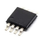
| 产品图片 |
|
| rohs | 符合RoHS无铅 / 符合限制有害物质指令(RoHS)规范要求 |
| 产品系列 | RF集成电路,射频检测器,Analog Devices AD8361ARMZ-REEL7* |
| 数据手册 | |
| 产品型号 | AD8361ARMZ-REEL7 |
| 产品种类 | 射频检测器 |
| 其它名称 | AD8361ARMZ-REEL7CT |
| 商标 | Analog Devices |
| 安装风格 | SMD/SMT |
| 封装 | Reel |
| 封装/箱体 | MSOP-8 |
| 工作电源电压 | 2.7 V to 5.5 V |
| 工厂包装数量 | 1000 |
| 最大功率耗散 | 200 mW |
| 最大工作温度 | + 85 C |
| 最大正向电压 | 2.7 V to 5.5 V |
| 最小工作温度 | - 40 C |
| 标准包装 | 1 |
| 系列 | AD8361 |
| 配置 | Single |
| 频率范围 | 100 MHz to 2500 MHz |


- 商务部:美国ITC正式对集成电路等产品启动337调查
- 曝三星4nm工艺存在良率问题 高通将骁龙8 Gen1或转产台积电
- 太阳诱电将投资9.5亿元在常州建新厂生产MLCC 预计2023年完工
- 英特尔发布欧洲新工厂建设计划 深化IDM 2.0 战略
- 台积电先进制程称霸业界 有大客户加持明年业绩稳了
- 达到5530亿美元!SIA预计今年全球半导体销售额将创下新高
- 英特尔拟将自动驾驶子公司Mobileye上市 估值或超500亿美元
- 三星加码芯片和SET,合并消费电子和移动部门,撤换高东真等 CEO
- 三星电子宣布重大人事变动 还合并消费电子和移动部门
- 海关总署:前11个月进口集成电路产品价值2.52万亿元 增长14.8%


PDF Datasheet 数据手册内容提取
LF to 2.5 GHz TruPwr™ Detector Data Sheet AD8361 FEATURES FUNCTIONAL BLOCK DIAGRAMS Calibrated rms response VPOS Excellent temperature stability i INTERNAL FILTER RFIN χ2 FLTR Up to 30 dB input range at 2.5 GHz TRANS- AD8361 700 mV rms, 10 dBm, re 50 Ω maximum input CONDUCTANCE CELLS ERROR ±0.25 dB linear response up to 2.5 GHz χ2 i AMP × 7.5 Single-supply operation: 2.7 V to 5.5 V BUFFER VRMS Low power: 3.3 mW at 3 V supply ADD Rapid power-down to less than 1 µA PWDN RBEAFNEDR-EGNACPE OFFSET SREF AMPeaPsLuIrCemATenIOt oNf SC DMA, W-CDMA, QAM, other complex IREF COMM 01088-C-002 modulation waveforms Figure 2. 8-Lead MSOP RF transmitter or receiver power measurement VPOS i INTERNAL FILTER RFIN χ2 FLTR GENERAL DESCRIPTION TRANS- AD8361 CONDUCTANCE The AD8361 is a mean-responding power detector for use in CELLS ERROR high frequency receiver and transmitter signal chains, up to χ2 i AMP × 7.5 BUFFER VRMS 2.5 GHz. It is very easy to apply. It requires a single supply only between 2.7 V and 5.5 V, a power supply decoupling capacitor, BAND-GAP and an input coupling capacitor in most applications. The PWDN REFERENCE oouf t7p.5u tV is/V a lrimnesa. rA-rne sepxotenrdnianlg f idltce rv ocaltpaagcei twoirt hca an c boen vaderdseiodn t og ain IREF COMM 01088-C-003 increase the averaging time constant. Figure 3. 6-Lead SOT-23 3.0 2.8 The AD8361 is intended for true power measurement of simple SUPPLY 2.6 REFERENCE MODE and complex waveforms. The device is particularly useful for 2.4 measuring high crest-factor (high peak-to-rms ratio) signals, 2.2 INTERNAL 2.0 REFERENCE MODE such as CDMA and W-CDMA. s) 1.8 Volt 1.6 The AD8361 has three operating modes to accommodate a ms ( 1.4 variety of analog-to-digital converter requirements: V r 1.2 REFEGRREONCUEN DMODE 1. Ground reference mode, in which the origin is zero. 1.0 0.8 2. Internal reference mode, which offsets the output 350 mV 0.6 above ground. 0.4 00..200 0.1 0.R2FIN (V rms0).3 0.4 0.5 01088-C-001 3Tan.h de iASsu Dapv8pa3liyl6a 1rb elifese sirnpe ne8cc-ielfe imeaddo fMdoerS, oOwpPhe iracanhtd ioo f6nf-s lfeertoasdm t hS −eO 4oT0u-°t2Cp3u t pto a t+oc8 kV5aSg°/Ce7s ..5 I.t Figure 1. Output in the Three Reference Modes, Supply 3 V, Frequency 1.9 GHz is fabricated on a proprietary high f silicon bipolar process. T (6-Lead SOT-23 Package Ground Reference Mode Only) Rev. F Document Feedback Information furnished by Analog Devices is believed to be accurate and reliable. However, no responsibility is assumed by Analog Devices for its use, nor for any infringements of patents or other One Technology Way, P.O. Box 9106, Norwood, MA 02062-9106, U.S.A. rights of third parties that may result from its use. Specifications subject to change without notice. No license is granted by implication or otherwise under any patent or patent rights of Analog Devices. Tel: 781.329.4700 ©1999–2015 Analog Devices, Inc. All rights reserved. Trademarks and registered trademarks are the property of their respective owners. Technical Support www.analog.com
AD8361 Data Sheet TABLE OF CONTENTS Features .............................................................................................. 1 Typical Performance Characteristics ..............................................6 Applications ....................................................................................... 1 Circuit Description......................................................................... 11 General Description ......................................................................... 1 Application Information ................................................................ 12 Functional Block Diagrams ............................................................. 1 Output Reference Temperature Drift Compensation ........... 16 Revision History ............................................................................... 2 Evaluation Board ............................................................................ 19 Specifications ..................................................................................... 3 Characterization Setups............................................................. 21 Absolute Maximum Ratings ............................................................ 4 Outline Dimensions ....................................................................... 22 ESD Caution .................................................................................. 4 Ordering Guide .......................................................................... 22 Pin Configuration and Function Descriptions ............................. 5 REVISION HISTORY 7/15—Rev. E to Rev. F 8/04—Rev. B to Rev. C Change to Ordering Guide ............................................................ 22 Changed Trimpots to Trimmable Potentiometers ......... Universal Changes to Specifications ................................................................. 3 5/15—Rev. D to Rev. E Changed Using the AD8361 Section Title to Applications ....... 12 Deleted Dynamic Range Extension for the AD8361 Section, Changes to Figure 43...................................................................... 14 Figure 60, Renumbered Sequentially ........................................... 19 Changes to Ordering Guide .......................................................... 24 Deleted Figure 61, Figure 62, Figure 63, and Figure 64 ............ 20 Updated Outline Dimensions ....................................................... 24 3/14—Rev. C to Rev. D Changes to Ordering Guide .......................................................... 24 Updated Outline Dimensions ....................................................... 24 Rev. F | Page 2 of 22
Data Sheet AD8361 SPECIFICATIONS T = 25°C, V = 3 V, f = 900 MHz, ground reference output mode, unless otherwise noted. A S RF Table 1. Parameter Condition Min Typ Max Unit SIGNAL INPUT INTERFACE (Input RFIN) Frequency Range1 2.5 GHz Linear Response Upper Limit V = 3 V 390 mV rms S Equivalent dBm, re 50 Ω 4.9 dBm V = 5 V 660 mV rms S Equivalent dBm, re 50 Ω 9.4 dBm Input Impedance2 225||1 Ω||pF RMS CONVERSION (Input RFIN to Output V rms) Conversion Gain 7.5 V/V rms f = 100 MHz, V = 5 V 6.5 8.5 V/V rms RF S Dynamic Range Error Referred to Best Fit Line3 ±0.25 dB Error4 CW Input, −40°C < T < +85°C 14 dB A ±1 dB Error CW Input, −40°C < T < +85°C 23 dB A ±2 dB Error CW Input, −40°C < T < +85°C 26 dB A CW Input, V = 5 V, −40°C < T < +85°C 30 dB S A Intercept-Induced Dynamic Internal Reference Mode 1 dB Range Reduction5, 6 Supply Reference Mode, V = 3.0 V 1 dB S Supply Reference Mode, V = 5.0 V 1.5 dB S Deviation from CW Response 5.5 dB Peak-to-Average Ratio (IS95 Reverse Link) 0.2 dB 12 dB Peak-to-Average Ratio (W-CDMA 4 Channels) 1.0 dB 18 dB Peak-to-Average Ratio (W-CDMA 15 Channels) 1.2 dB OUTPUT INTERCEPT5 Inferred from Best Fit Line3 Ground Reference Mode (GRM) 0 V at SREF, V at IREF 0 V S f = 100 MHz, V = 5 V −50 +150 mV RF S Internal Reference Mode (IRM) 0 V at SREF, IREF Open 350 mV f = 100 MHz, V = 5 V 300 500 mV RF S Supply Reference Mode (SRM) 3 V at IREF, 3 V at SREF 400 mV V at IREF, V at SREF V/7.5 V S S S f = 100 MHz, V = 5 V 590 750 mV RF S POWER-DOWN INTERFACE PWDN HI Threshold 2.7 ≤ V ≤ 5.5 V, −40°C < T < +85°C V − 0.5 V S A S PWDN LO Threshold 2.7 ≤ V ≤ 5.5 V, −40°C < T < +85°C 0.1 V S A Power-Up Response Time 2 pF at FLTR Pin, 224 mV rms at RFIN 5 μs 100 nF at FLTR Pin, 224 mV rms at RFIN 320 μs PWDN Bias Current <1 μA POWER SUPPLIES Operating Range −40°C < T < +85°C 2.7 5.5 V A Quiescent Current 0 mV rms at RFIN, PWDN Input LO7 1.1 mA Power-Down Current GRM or IRM, 0 mV rms at RFIN, PWDN Input HI <1 μA SRM, 0 mV rms at RFIN, PWDN Input HI 10 × V μA S 1 Operation at arbitrarily low frequencies is possible; see Application Information section. 2 Figure 17 and Figure 47 show impedance versus frequency for the MSOP and SOT-23, respectively. 3 Calculated using linear regression. 4 Compensated for output reference temperature drift; see Application Information section. 5 SOT-23-6L operates in ground reference mode only. 6 The available output swing, and hence the dynamic range, is altered by both supply voltage and reference mode; see Figure 39 and Figure 40. 7 Supply current is input level dependent; see Figure 16. Rev. F | Page 3 of 22
AD8361 Data Sheet ABSOLUTE MAXIMUM RATINGS Stresses at or above those listed under Absolute Maximum Table 2. Ratings may cause permanent damage to the product. This is a Parameter Rating stress rating only; functional operation of the product at these Supply Voltage V 5.5 V S or any other conditions above those indicated in the SREF, PWDN 0 V, V S operational section of this specification is not implied. IREF V − 0.3 V, V S S Operation beyond the maximum operating conditions for RFIN 1 V rms extended periods may affect product reliability. Equivalent Power, re 50 Ω 13 dBm ESD CAUTION Internal Power Dissipation1 200 mW 6-Lead SOT-23 170 mW 8-Lead MSOP 200 mW Maximum Junction Temperature 125°C Operating Temperature Range −40°C to +85°C Storage Temperature Range −65°C to +150°C Lead Temperature Range 300°C (Soldering 60 sec) 1 Specification is for the device in free air. 6-Lead SOT-23: θJA = 230°C/W; θJC = 92°C/W. 8-Lead MSOP: θJA = 200°C/W; θJC = 44°C/W. Rev. F | Page 4 of 22
Data Sheet AD8361 PIN CONFIGURATION AND FUNCTION DESCRIPTIONS VRMS 1 6 VPOS VPOS 1 8 SREF AD8361 AD8361 IREF 2 7 VRMS COMM 2 TOP VIEW 5 RFIN PWRFDINN 34 (NToOt Pto V SIEcaWle) 65 FCLOTMRM 01088-C-004 FLTR 3 (Not to Scale) 4 PWDN 01088-C-005 Figure 4. 8-Lead MSOP Figure 5. 6-Lead SOT-23 Table 3. Pin Function Descriptions Pin No. Pin No. MSOP SOT-23 Mnemonic Description 1 6 VPOS Supply Voltage Pin. Operational range 2.7 V to 5.5 V. 2 N/A IREF Output Reference Control Pin. Internal reference mode enabled when pin is left open; otherwise, this pin should be tied to VPOS. Do not ground this pin. 3 5 RFIN Signal Input Pin. Must be driven from an ac-coupled source. The low frequency real input impedance is 225 Ω. 4 4 PWDN Power-Down Pin. For the device to operate as a detector, it needs a logical low input (less than 100 mV). When a logic high (greater than V − 0.5 V) is applied, the device is turned off and the supply S current goes to nearly zero (ground and internal reference mode less than 1 µA, supply reference mode V divided by 100 kΩ). S 5 2 COMM Device Ground Pin. 6 3 FLTR By placing a capacitor between this pin and VPOS, the corner frequency of the modulation filter is lowered. The on-chip filter is formed with 27 pF||2 kΩ for small input signals. 7 1 VRMS Output Pin. Near rail-to-rail voltage output with limited current drive capabilities. Expected load >10 kΩ to ground. 8 N/A SREF Supply Reference Control Pin. To enable supply reference mode, this pin must be connected to VPOS; otherwise, it should be connected to COMM (ground). Rev. F | Page 5 of 22
AD8361 Data Sheet TYPICAL PERFORMANCE CHARACTERISTICS 2.8 3.0 2.6 900MHz 2.5 2.4 2.0 2.2 100MHz 1900MHz 1.5 2.0 1.8 1.0 PUT (V) 11..46 2.5GHz OR (dB) 0.50 OUT 1.2 ERR–0.5 1.0 –1.0 0.8 MEAN±3 SIGMA –1.5 0.6 0.4 –2.0 0.2 –2.5 0.00 0.1 0.I2NPUT (V rm0s.3) 0.4 0.5 01088-C-006 –3.00.01 (–201.d0B2m) INPUT (V( –r7m0d.sB1)m) (+50d.B4m) 01088-C-009 Figure 6. Output vs. Input Level, Frequencies 100 MHz, 900 MHz, Figure 9. Error from Linear Reference vs. Input Level, 3 Sigma to Either Side of 1900 MHz, and 2500 MHz, Supply 2.7 V, Ground Reference Mode, MSOP Mean, Sine Wave, Supply 3.0 V, Frequency 900 MHz 5.5 5.5V 3.0 5.0 2.5 4.5 2.0 5.0V 4.0 1.5 3.0V 3.5 1.0 UTPUT (V)32..05 ROR (dB)0.50 O R–0.5 2.0 2.7V E –1.0 1.5 MEAN±3 SIGMA –1.5 1.0 –2.0 0.5 –2.5 0.00 0.1 0.2 0.3INPUT0 . 4(V rms0).5 0.6 0.7 0.8 01088-C-007 –3.00.01 (–201.d0B2m) INP(U–7T0d (.B1Vm rm)s) (+8.06.d6Bm) 01088-C-010 Figure 7. Output vs. Input Level, Figure 10. Error from Linear Reference vs. Input Level, 3 Sigma to Either Side Supply 2.7 V, 3.0 V, 5.0 V, and 5.5 V, Frequency 900 MHz of Mean, Sine Wave, Supply 5.0 V, Frequency 900 MHz 5.0 3.0 CW IS95 2.5 4.5 REVERSE LINK 2.0 4.0 1.5 3.5 IS95 1.0 CW REVERSE LINK OUTPUT (V)322...050 4- ANDW 1C5D-CMHAANNEL ERROR (dB)–000...550 4-CHANNEL –1.0 1.5 –1.5 15-CHANNEL 1.0 –2.0 0.5 –2.5 0.00 0.1 0.2 0.3INPUT0 .(4V rms)0.5 0.6 0.7 0.8 01088-C-008 –3.00.01 0.02 INPUT0 .(1V rms) 0.2 0.6 1.0 01088-C-011 Figure 11. Error from CW Linear Reference vs. Input with Different Figure 8. Output vs. Input Level with Waveforms Sine Wave (CW), IS95 Reverse Link, W-CDMA 4-Channel and Different Waveforms Sine Wave (CW), IS95 Reverse Link, W-CDMA 15-Channel, Supply 3.0 V, Frequency 900 MHz W-CDMA 4-Channel and W-CDMA 15-Channel, Supply 5.0 V Rev. F | Page 6 of 22
Data Sheet AD8361 3.0 3.0 2.5 2.5 2.0 2.0 1.5 1.5 +85°C 1.0 1.0 B) 0.5 B) 0.5 d d OR ( 0 OR ( 0 R R R–0.5 R–0.5 E E –1.0 –1.0 MEAN3 SIGMA –40°C –1.5 –1.5 –2.0 –2.0 2.5 –2.5 –3.00.01 (–201.d0B2m) INPUT (V( –r7m0d.sB1)m) (+50d.B4m) 01088-C-012 –3.00.01 (–201.d0B2m) INPUT (V( –r7m0d.sB1)m) (+50d.B4m) 01088-C-015 Figure 12. Error from CW Linear Reference vs. Input, 3 Sigma to Either Side of Figure 15. Output Delta from +25°C vs. Input Level, 3 Sigma to Either Mean, IS95 Reverse Link Signal, Supply 3.0 V, Frequency 900 MHz Side of Mean Sine Wave, Supply 3.0 V, Frequency 1900 MHz, Temperature −40°C to +85°C 3.0 11 2.5 10 VS = 5V INPUT OUT 2.0 9 OF RANGE 1.5 A) 8 –40°C +25°C m 1.0 T ( 7 VS = 3V ROR (dB)0.05 CURREN 65 IONFP URTA NOGUET +85°C R–0.5 Y +25°C E PL 4 –1.0 P MEAN3 SIGMA SU 3 +85°C –1.5 –2.0 2 ––23..500.01 (–201.d0B2m) INP(U–7T0d (.B1Vm rm)s) (+8.06.d6Bm) 01088-C-013 100 0.1–40°0C.2 0.3INPUT0 .(4V rms)0.5 0.6 0.7 0.8 01088-C-016 Figure 13. Error from CW Linear Reference vs. Input Level, 3 Sigma to Either Figure 16. Supply Current vs. Input Level, Supplies 3.0 V, and 5.0 V, Side of Mean, IS95 Reverse Link Signal, Supply 5.0 V, Frequency 900 MHz Temperatures −40°C, +25°C, and +85°C 3.0 250 1.8 +25°C 2.5 +85°C 1.6 2.0 200 ERROR (dB)––10101.....005550 +85°C UNT RESISTANCE ()110500 +–2450°C°C +85°C 111...420 NT CAPACITANCE (pF) –1.5 –40°C SH –40°C 0.8 SHU 50 –2.0 0.6 –2.5 –3.00.01 (–201.d0B2m) INPUT (V(– r7m0d.sB1)m) (+50d.B4m) 01088-C-014 00 500 F1R0E0Q0UENCY 1(M50H0z) 2000 25000.4 01088-C-017 Figure 14. Output Delta from +25°C vs. Input Level, 3 Sigma to Figure 17. Input Impedance vs. Frequency, Supply 3 V, Either Side of Mean Sine Wave, Supply 3.0 V, Temperatures −40°C, +25°C, and +85°C, MSOP Frequency 900 MHz, Temperature −40°C to +85°C (See the Application Information Section for SOT-23 Data) Rev. F | Page 7 of 22
AD8361 Data Sheet 0.03 0.18 0.16 0.02 0.14 HANGE (V) 00..0010 E (V/V rms) 000...101280 MEAN±3 SIGMA EPT C–0.01 HANG 00..0064 TERC–0.02 MEAN±3 SIGMA AIN C 0.02 IN–0.03 G 0.00 –0.02 –0.04 –0.04 –0.05 –40 –20 0TEMPE2R0ATURE4 0(°C) 60 80 100 01088-C-018 –0.06 –40 –20 0TEMPE2R0ATURE4 0(°C) 60 80 100 01088-C-021 Figure 18. Output Reference Change vs. Temperature, Figure 21. Conversion Gain Change vs. Temperature, Supply 3 V, Supply 3 V, Ground Reference Mode Ground Reference Mode, Frequency 900 MHz 0.02 0.18 0.16 0.14 0.01 0.12 GE (V) V rms) 0.10 MEAN±3 SIGMA HAN 0.00 E (V/ 0.08 C G 0.06 CEPT –0.01 CHAN 0.04 TER MEAN±3 SIGMA AIN 0.02 IN G 0.00 –0.02 –0.02 –0.04 –0.03 –40 –20 0TEMPE2R0ATURE4 0(°C) 60 80 100 01088-C-019 –0.06 –40 –20 0TEMPE2R0ATURE4 0(°C) 60 80 100 01088-C-022 Figure 19. Output Reference Change vs. Temperature, Supply 3 V, Figure 22. Conversion Gain Change vs. Temperature, Supply 3 V, Internal Reference Mode (MSOP Only) Internal Reference Mode, Frequency 900 MHz (MSOP Only) 0.03 0.18 0.16 0.02 0.14 E (V) 0.01 ms) 00..1120 ANG 0.00 V/V r 0.08 MEAN±3 SIGMA RCEPT CH––00..0012 CHANGE ( 00..0064 NTE MEAN±3 SIGMA AIN 0.02 I–0.03 G 0.00 –0.02 –0.04 –0.04 –0.05 –40 –20 0TEMPE2R0ATURE4 0(°C) 60 80 100 01088-C-020 –0.06 –40 –20 0TEMPE2R0ATURE4 0(°C) 60 80 100 01088-C-023 Figure 20. Output Reference Change vs. Temperature, Supply 3 V, Figure 23. Conversion Gain Change vs. Temperature, Supply 3 V, Supply Reference Mode (MSOP Only) Supply Reference Mode, Frequency 900 MHz (MSOP Only) Rev. F | Page 8 of 22
Data Sheet AD8361 GATE PULSE FOR PWDN INPUT 900MHz RF TONE 370mV 500mV PER 370mV VERTICAL DIVISION 270mV 500mV PER 270mV VERTICAL DIVISION RF INPUT RF INPUT 67mV 67mV 5µs PER HORIZONTA25Lm DVIVISION 01088-C-024 2µs PER HORIZONTAL DIV2I5SmIOVN 01088-C-027 Figure 24. Output Response to Modulated Pulse Input for Various RF Input Figure 27. Output Response Using Power-Down Mode for Various RF Input Levels, Supply 3 V, Modulation Frequency 900 MHz, No Filter Capacitor Levels, Supply 3 V, Frequency 900 MHz, No Filter Capacitor GATEPULSEFOR 900MHzRFTONE PWDN INPUT 370mV 500mV PER 370mV VERTICAL DIVISION 270mV 270mV 500mV PER VERTICAL RF INPUT DIVISION RF INPUT 67mV 67mV 50µs PER HORIZONT2A5Lm DVIVISION 01088-C-025 20µs PER HORIZONTAL DIVISI2O5NmV 01088-C-028 Figure 25. Output Response to Modulated Pulse Input for Various RF Input Figure 28. Output Response Using Power-Down Mode for Various RF Input Levels, Supply 3 V, Modulation Frequency 900 MHz, 0.01 µF Filter Capacitor Levels, Supply 3 V, Frequency 900 MHz, 0.01 µF Filter Capacitor HPE3631A HPE3631A POWER SUPPLY TEK TDS784C POWER SUPPLY TEK TDS784C SCOPE SCOPE 0.01CµF4 100CpF2 1 VPOASD836S1REF 8 0.01CµF4 100CpF2 1 VPOASD836S1REF 8 C1 2 IREF VRMS 7 C3 FTEETK P PR6O20B4E C1 2 IREF VRMS 7 C3 FTEETK P PR6O20B4E 3 RFIN FLTR 6 C5 3 RFIN FLTR 6 C5 75RΩ1 0.1µF 4 PWDN COMM 5 100pF 75RΩ1 0.1µF 4 PWDN COMM 5 100pF GEHSNPIEG8R6N4AA8TLBOR 01088-C-026 GEHSNPIEG8R6N4AA8TLBOR GEHSNPIEG8R1N1AA0TLAOR 01088-C-029 Figure 26. Hardware Configuration for Figure 29. Hardware Configuration Output Response to Modulated Pulse Input for Output Response Using Power-Down Mode Rev. F | Page 9 of 22
AD8361 Data Sheet 7.8 16 7.6 14 7.4 VS= 3V ms) 7.2 12 V r AIN (V/ 67..80 ENT10 SION G 6.6 PERC 8 R 6.4 6 E V ON 6.2 4 C 6.0 2 5.8 5.6100 CARRIER FREQUENCY (M1H0z0)0 01088-C-030 06.9 7.0 CONV7E.2RSION GA7IN.4 (V/V rms)7.6 7.8 01088-C-033 Figure 30. Conversion Gain Change vs. Frequency, Supply 3 V, Ground Figure 33. Conversion Gain Distribution Frequency 100 MHz, Reference Mode, Frequency 100 MHz to 2500 MHz, Representative Device Supply 5 V, Sample Size 3000 SUPPLY RF 12 INPUT 370mV 500mV PER VERTICAL 10 DIVISION 270mV T 8 N E C R E 6 P 67mV 4 20µs PER HORIZONT2A5Lm DVIVISION 01088-C-031 20 0.32 0.34 IREF0. 3M6ODE I0N.3T8ERCEP0.T4 0(V) 0.42 0.44 01088-C-034 Figure 31. Output Response to Gating on Power Supply, for Various RF Input Figure 34. Output Reference, Internal Reference Mode, Supply 5 V, Levels, Supply 3 V, Modulation Frequency 900 MHz, 0.01 µF Filter Capacitor Sample Size 3000 (MSOP Only) 12 AD811 HP8110A PULSE 50Ω GENERATOR 10 732Ω TEK TDS784C 8 SCOPE NT E C R 6 0.01CµF4 100CpF2 AD8361 PE 1 VPOS SREF 8 4 TEK P6204 2 IREF VRMS 7 FET PROBE C1 C3 3 RFIN FLTR 6 C5 2 R1 0.1µF 100pF GEHSNPIEG8R6N4AA78T5LBOΩR 4 PWDN COMM 5 01088-C-032 0 0.64 0.66 SR0E.6F8 MODE0 I.N7T0ERCE0P.T72 (V) 0.74 0.76 01088-C-035 Figure 32. Hardware Configuration for Output Response to Power Supply Figure 35. Output Reference, Supply Reference Mode, Supply 5 V, Gating Measurements Sample Size 3000 (MSOP Only) Rev. F | Page 10 of 22
Data Sheet AD8361 CIRCUIT DESCRIPTION The AD8361 is an rms-responding (mean power) detector that The squaring cells have very wide bandwidth with an intrinsic provides an approach to the exact measurement of RF power response from dc to microwave. However, the dynamic range of that is basically independent of waveform. It achieves this such a system is fairly small, due in part to the much larger function through the use of a proprietary technique in which dynamic range at the output of the squaring cells. There are the outputs of two identical squaring cells are balanced by the practical limitations to the accuracy of sensing very small error action of a high-gain error amplifier. signals at the bottom end of the dynamic range, arising from small random offsets that limit the attainable accuracy at small inputs. The signal to be measured is applied to the input of the first squaring cell, which presents a nominal (LF) resistance of 225 Ω On the other hand, the squaring cells in the AD8361 have a between the RFIN and COMM pins (connected to the ground Class-AB aspect; the peak input is not limited by their quiescent plane). Because the input pin is at a bias voltage of about 0.8 V bias condition but is determined mainly by the eventual loss of above ground, a coupling capacitor is required. By making this square-law conformance. Consequently, the top end of their an external component, the measurement range may be response range occurs at a fairly large input level (approximately extended to arbitrarily low frequencies. 700 mV rms) while preserving a reasonably accurate square-law response. The maximum usable range is, in practice, limited by The AD8361 responds to the voltage, V , at its input by IN the output swing. The rail-to-rail output stage can swing from a squaring this voltage to generate a current proportional to V IN few millivolts above ground to less than 100 mV below the squared. This is applied to an internal load resistor, across supply. An example of the output induced limit: given a gain of which a capacitor is connected. These form a low-pass filter, 7.5 and assuming a maximum output of 2.9 V with a 3 V which extracts the mean of V squared. Although essentially IN supply, the maximum input is (2.9 V rms)/7.5 or 390 mV rms. voltage-responding, the associated input impedance calibrates this port in terms of equivalent power. Therefore, 1 mW Filtering corresponds to a voltage input of 447 mV rms. The Application An important aspect of rms-dc conversion is the need for Information section shows how to match this input to 50 Ω. averaging (the function is root-MEAN-square). For complex RF The voltage across the low-pass filter, whose frequency may be waveforms, such as those that occur in CDMA, the filtering arbitrarily low, is applied to one input of an error-sensing amplifier. provided by the on-chip, low-pass filter, although satisfactory A second identical voltage-squaring cell is used to close a negative for CW signals above 100 MHz, is inadequate when the signal feedback loop around this error amplifier. This second cell is has modulation components that extend down into the driven by a fraction of the quasi-dc output voltage of the kilohertz region. For this reason, the FLTR pin is provided: a AD8361. When the voltage at the input of the second squaring capacitor attached between this pin and VPOS can extend the cell is equal to the rms value of V , the loop is in a stable state, averaging time to very low frequencies. IN and the output then represents the rms value of the input. The Offset feedback ratio is nominally 0.133, making the rms-dc An offset voltage can be added to the output (when using the conversion gain ×7.5, that is MSOP version) to allow the use of ADCs whose range does not VOUT 7.5VINrms extend down to ground. However, accuracy at the low end degrades because of the inherent error in this added voltage. By completing the feedback path through a second squaring This requires that the IREF (internal reference) pin be tied to cell, identical to the one receiving the signal to be measured, VPOS and SREF (supply reference) to ground. several benefits arise. First, scaling effects in these cells cancel; thus, the overall calibration may be accurate, even though the In the IREF mode, the intercept is generated by an internal open-loop response of the squaring cells taken separately need reference cell and is a fixed 350 mV, independent of the supply not be. Note that in implementing rms-dc conversion, no voltage. To enable this intercept, IREF should be open-circuited, reference voltage enters into the closed-loop scaling. Second, and SREF should be grounded. the tracking in the responses of the dual cells remains very close In the SREF mode, the voltage is provided by the supply. To over temperature, leading to excellent stability of calibration. implement this mode, tie IREF to VPOS and SREF to VPOS. The offset is then proportional to the supply voltage and is 400 mV for a 3 V supply and 667 mV for a 5 V supply. Rev. F | Page 11 of 22
AD8361 Data Sheet APPLICATION INFORMATION Basic Connections +VS 2.7V– 5.5V Figure 36 through Figure 38 show the basic connections for the AD8361’s MSOP version in its three operating modes. In all 100pF modes, the device is powered by a single supply of between 0.01F AD8361 2.7 V and 5.5 V. The VPOS pin is decoupled using 100 pF and 1 VPOS SREF 8 0.01 μF capacitors. The quiescent current of 1.1 mA in CC 2 IREF VRMS 7 V rms operating mode can be reduced to 1 μA by pulling the PWDN 100pF RFIN 3 RFIN FLTR 6 pAi n7 5u pΩ t eox VtePrnOaSl .s hunt resistance combines with the ac-coupled 75R1 4 PWDN COMM 5 CFLTR 01088-C-038 input to give an overall broadband input impedance near 50 Ω. Figure 38. Basic Connections for Supply Referenced Mode Note that the coupling capacitor must be placed between the The output voltage is nominally 7.5 times the input rms voltage input and the shunt impedance. Input impedance and input (a conversion gain of 7.5 V/V rms). Three modes of operation coupling are discussed in more detail below. are set by the SREF and IREF pins. In addition to the ground The input coupling capacitor combines with the internal input reference mode shown in Figure 36, where the output voltage resistance (Figure 37) to provide a high-pass corner frequency swings from around near ground to 4.9 V on a 5.0 V supply, two given by the equation additional modes allow an offset voltage to be added to the 1 output. In the internal reference mode (Figure 37), the output f3dB 2πC R voltage swing is shifted upward by an internal reference voltage C IN of 350 mV. In supply referenced mode (Figure 38), an offset With the 100 pF capacitor shown in Figure 36 through Figure 38, voltage of V/7.5 is added to the output voltage. Table 4 S the high-pass corner frequency is about 8 MHz. summarizes the connections, output transfer function, and +VS 2.7V– 5.5V minimum output voltage (i.e., zero signal) for each mode. Output Swing 100pF Figure 39 shows the output swing of the AD8361 for a 5 V 0.01F AD8361 supply voltage for each of the three modes. It is clear from 1 VPOS SREF 8 Figure 39 that operating the device in either internal reference CC 2 IREF VRMS 7 V rms mode or supply referenced mode reduces the effective dynamic 100pF range as the output headroom decreases. The response for lower RFIN 3 RFIN FLTR 6 75R1 4 PWDN COMM 5 CFLTR 01088-C-036 souffpspetly i sv somltaaglleesr )is, bsiumt tilhaer d(iynn tahme iscu rpapnlgye r reefedruecnecse fdu mrthoedre a, sth e Figure 36. Basic Connections for Ground Reference Mode headroom decreases. Figure 40 shows the response of the AD8361 to a CW input for various supply voltages. +VS 2.7V– 5.5V 5.0 SUPPLY REF 4.5 100pF 4.0 INTERNAL REF 0.01F AD8361 3.5 1 VPOS SREF 8 V) 3.0 GROUND REF 10C0CpF 2 IREF VRMS 7 V rms PUT ( 2.5 T RFIN 75R1 34 RPWFINDN CFOLMTMR 65 CFLTR 01088-C-037 OU 12..50 Figure 37. Basic Connections for Internal Reference Mode 1.0 0.5 0.00 0.1 0.2 0.3INPUT0 (.4V rms)0.5 0.6 0.7 0.8 01088-C-039 Figure 39. Output Swing for Ground, Internal, and Supply Referenced Mode, VPOS = 5 V (MSOP Only) Rev. F | Page 12 of 22
Data Sheet AD8361 5.5 5.5V should however be noted that offsets at the low end can be 5.0 either positive or negative, so this plot could also trend upwards 4.5 at the low end. Figure 9, Figure 10, Figure 12, and Figure 13 5.0V 4.0 show a ±3 sigma distribution of the device error for a large 3.0V 3.5 population of devices. V) T ( 3.0 2.0 U UTP 2.5 1.5 O 2.0 2.7V 1.0 1.5 2.5GHz 1.0 B) 0.5 00..500 0.1 0.2 0.3INPUT0 .(4V rms)0.5 0.6 0.7 0.8 01088-C-040 ERROR (d–00..50 100MHz 100MHz 1.9GHz Figure 40. Output Swing for Supply Voltages of –1.0 2.7 V, 3.0 V, 5.0 V and 5.5 V (MSOP Only) –1.5 Dynamic Range 900MHz nBoemcaiunsael tthraen AsfDer8 3fu6n1 citsi oan li nofe a7r.5-r Ves/pVo nrmdisn,g t hdee vdiycne awmitihc raa nge in –2.00.01 (–201.d0B2m) INP(U–7T0d (.B1Vm rm)s) (+50d.B4m) 1.0 01088-C-042 dB is not clear from plots such as Figure 39. As the input level is Figure 42. Representative Unit, Error in dB vs. Input Level, VS = 2.7 V increased in constant dB steps, the output step size (per dB) also increases. Figure 41 shows the relationship between the output It is also apparent in Figure 42 that the error plot tends to shift step size (i.e., mV/dB) and input voltage for a nominal transfer to the right with increasing frequency. Because the input function of 7.5 V/V rms. impedance decreases with frequency, the voltage actually applied to the input also tends to decrease (assuming a constant Table 4. Connections and Nominal Transfer Function for source impedance over frequency). The dynamic range is Ground, Internal, and Supply Reference Modes almost constant over frequency, but with a small decrease in Output conversion gain at high frequency. Reference Intercept Input Coupling and Matching Mode IREF SREF (No Signal) Output Ground VPOS COMM Zero 7.5 V The input impedance of the AD8361 decreases with increasing IN Internal OPEN COMM 0.350 V 7.5 V + 0.350 V frequency in both its resistive and capacitive components IN Supply VPOS VPOS V/7.5 7.5 V + V/7.5 (Figure 17). The resistive component varies from 225 Ω at S IN S 100 MHz down to about 95 Ω at 2.5 GHz. 700 A number of options exist for input matching. For operation at multiple frequencies, a 75 Ω shunt to ground, as shown in 600 Figure 43, provides the best overall match. For use at a single frequency, a resistive or a reactive match can be used. By 500 plotting the input impedance on a Smith Chart, the best value B400 for a resistive match can be calculated. The VSWR can be held d V/ below 1.5 at frequencies up to 1 GHz, even as the input m 300 impedance varies from part to part. (Both input impedance and input capacitance can vary by up to ±20% around their nominal 200 values.) At very high frequencies (i.e., 1.8 GHz to 2.5 GHz), a 100 shunt resistor is not sufficient to reduce the VSWR below 1.5. 00 100 200 300INPU4T0 0(mV)500 600 700 800 01088-C-041 Wisnhsohewerrtne a iVnn S iFnWidgRuuc riteso 4crr 4ii.nt i csaelr,i eres mwoitvhe tthhee csohuupnlti ncgo mcappoancietnotr aans d Figure 41. Idealized Output Step Size as a Function of Input Voltage Table 5 gives recommended shunt resistor values for various Plots of output voltage versus input voltage result in a straight frequencies and series inductor values for high frequencies. The line. It may sometimes be more useful to plot the error on a coupling capacitor, C , essentially acts as an ac-short and plays C logarithmic scale, as shown in Figure 42. The deviation of the no intentional part in the matching. plot for the ideal straight line characteristic is caused by output clipping at the high end and by signal offsets at the low end. It Rev. F | Page 13 of 22
AD8361 Data Sheet Table 6. Recommended Values for a Reactive Input CC Matching (Figure 45) RFIN RFIN RSH AD8361 01088-C-043 F1r0e0q uency (MHz) C16M (pF) L1M80 ( n H) Figure 43. Input Coupling/Matching Options, Broadband Resistor Match 800 2 15 900 2 12 1800 1.5 4.7 LM CC RFIN RFIN 1900 1.5 4.7 AD8361 01088-C-044 2 500 1.5 3.3 Figure 44. Input Coupling/Matching Options, Series Inductor Match Input Coupling Using a Series Resistor Figure 46 shows a technique for coupling the input signal into the AD8361 that may be applicable where the input signal is CM CC RFIN RFIN much larger than the input range of the AD8361. A series LM AD8361 01088-C-045 raettseisntuoart ceo tmheb iinnpesu tw siitghn tahl.e Binepcauut siem tpheisd saenrciee so rfe tshiset oArD fo8r3m61s tao divider with the frequency dependent input impedance, the Figure 45. Input Coupling/Matching Options, Narrowband Reactive Match apparent gain changes greatly with frequency. However, this method has the advantage of very little power being tapped off in RF power transmission applications. If the resistor is large RSERIES CC RFIN RFIN compared to the transmission line’s impedance, then the VSWR AD8361 01088-C-046 of th25e0 system is relatively unaffected. 1.7 Figure 46. Input Coupling/Matching Options, Attenuating the Input Signal Table 5. Recommended Component Values for Resistive or 200 1.4 Inductive Input Matching (Figure 43 and Figure 44) Frequency Matching Component ) pF) 180000 MMHHzz 6735. 4Ω ΩSh Suhnutn t STANCE (150 1.1 CITANCE ( 900 MHz 75 Ω Shunt ESI100 0.8 PA R A 1800 MHz 150 Ω Shunt or 4.7 nH Series C 1900 MHz 150 Ω Shunt or 4.7 nH Series 50 0.5 2500 MHz 150 Ω Shunt or 2.7 nH Series Ainldteurcntoatri vtoel yg,r ao urenadc tainved ma saetcrihe sc acnap baec iitmorp, laesm sehnotwedn uinsi nFgig au rseh u45n.t A 00 500 1000 FRE15Q0U0ENCY20 (0M0Hz) 2500 3000 35000.2 01088-C-047 method for hand calculating the appropriate matching components Figure 47. Input Impedance vs. Frequency, Supply 3 V, SOT-23 is shown on page 12 of the AD8306 data sheet. Selecting the Filter Capacitor Matching in this manner results in very small values for C , M The AD8361’s internal 27 pF filter capacitor is connected in especially at high frequencies. As a result, a stray capacitance as parallel with an internal resistance that varies with signal level small as 1 pF can significantly degrade the quality of the match. from 2 kΩ for small signals to 500 Ω for large signals. The The main advantage of a reactive match is the increase in resulting low-pass corner frequency between 3 MHz and sensitivity that results from the input voltage being gained up 12 MHz provides adequate filtering for all frequencies above (by the square root of the impedance ratio) by the matching 240 MHz (i.e., 10 times the frequency at the output of the network. Table 6 shows the recommended values for reactive squarer, which is twice the input frequency). However, signals matching. with high peak-to-average ratios, such as CDMA or W-CDMA signals, and low frequency components require additional filtering. TDMA signals, such as GSM, PDC, or PHS, have a peak-to average ratio that is close to that of a sinusoid, and the internal filter is adequate. Rev. F | Page 14 of 22
Data Sheet AD8361 The filter capacitance of the AD8361 can be augmented by The AD8361 can be disabled either by pulling the PWDN connecting a capacitor between Pin 6 (FLTR) and VPOS. Table 7 (Pin 4) to VPOS or by simply turning off the power to the shows the effect of several capacitor values for various device. While turning off the device obviously eliminates the communications standards with high peak-to-average ratios current consumption, disabling the device reduces the leakage along with the residual ripple at the output, in peak-to-peak and current to less than 1 μA. Figure 27 and Figure 28 show the rms volts. Note that large filter capacitors increase the enable and response of the output of the AD8361 to a pulse on the PWDN pulse response times, as discussed below. pin, with no capacitance and with a filter capacitance of 0.01 μF, respectively; the turn-on time is a function of the filter Table 7. Effect of Waveform and CFILT on Residual AC capacitor. Figure 31 shows a plot of the output response to the Output Residual AC supply being turned on (i.e., PWDN is grounded and VPOS is Waveform CFILT V dc mV p-p mV rms pulsed) with a filter capacitor of 0.01 μF. Again, the turn-on IS95 Reverse Link Open 0.5 550 100 time is strongly influenced by the size of the filter capacitor. 1.0 1000 180 If the input of the AD8361 is driven while the device is disabled 2.0 2000 360 (PWDN = VPOS), the leakage current of less than 1 μA increases 0.01 μF 0.5 40 6 as a function of input level. When the device is disabled, the 1.0 160 20 output impedance increases to approximately 16 kΩ. 2.0 430 60 0.1 μF 0.5 20 3 Volts to dBm Conversion 1.0 40 6 In many of the plots, the horizontal axis is scaled in both rms 2.0 110 18 volts and dBm. In all cases, dBm are calculated relative to an IS95 8-Channel 0.01 μF 0.5 290 40 impedance of 50 Ω. To convert between dBm and volts in a Forward Link 1.0 975 150 50 Ω system, the following equations can be used. Figure 48 2.0 2600 430 shows this conversion in graphical form. 0.1 μF 0.5 50 7 Vrms2 1.0 190 30 2.0 670 95 PowerdBm10log 50Ω 10log20Vrms2 W-CDMA 15 0.01 μF 0.5 225 35 0.001W Channel 1.0 940 135 2.0 2500 390 0.1 μF 0.5 45 6 dBm log1dBm/10 Vrms 0.001W50Ωlog1 1.0 165 25 10 20 2.0 550 80 V rms dBm Operation at Low Frequencies +20 Although the AD8361 is specified for operation up to 2.5 GHz, 1 +10 there is no lower limit on the operating frequency. It is only 0 necessary to increase the input coupling capacitor to reduce the 0.1 corner frequency of the input high-pass filter (use an input –10 resistance of 225 Ω for frequencies below 100 MHz). It is also –20 necessary to increase the filter capacitor so that the signal at 0.01 –30 the output of the squaring circuit is free of ripple. The corner forfe 2q ukeΩn cayn dis tsheet bexyt tehren aclo fmiltbeirn caatipoanc iotaf nthcee. internal resistance 0.001 –40 01088-C-048 Power Consumption, Enable and Power-On Figure 48. Conversion from dBm to rms Volts The quiescent current consumption of the AD8361 varies with the size of the input signal from about 1 mA for no signal up to 7 mA at an input level of 0.66 V rms (9.4 dBm, re 50 Ω). If the input is driven beyond this point, the supply current increases steeply (see Figure 16). There is little variation in quiescent current with power supply voltage. Rev. F | Page 15 of 22
AD8361 Data Sheet Output Drive Capability and Buffering OUTPUT REFERENCE TEMPERATURE DRIFT COMPENSATION The AD8361 is capable of sourcing an output current of approximately 3 mA. If additional current is required, a simple The error due to low temperature drift of the AD8361 can be buffering circuit can be used as shown in Figure 51. Similar reduced if the temperature is known. Many systems incorporate circuits can be used to increase or decrease the nominal conversion a temperature sensor; the output of the sensor is typically gain of 7.5 V/V rms (Figure 49 and Figure 50). In Figure 50, the digitized, facilitating a software correction. Using this information, AD8031 buffers a resistive divider to give a slope of 3.75 V/V only a two-point calibration at ambient is required. rms. In Figure 49, the op amp’s gain of two increases the slope The output voltage of the AD8361 at ambient (25°C) can be to 15 V/V rms. Using other resistor values, the slope can be expressed by the equation changed to an arbitrary value. The AD8031 rail-to-rail op amp, used in these example, can swing from 50 mV to 4.95 V on a VOUT =(GAIN×VIN)+ςΟΣ single 5 V supply and operate at supply voltages down to 2.7 V. where GAIN is the conversion gain in V/V rms and V is the OS If high output current is required (>10 mA), the AD8051, which extrapolated output voltage for an input level of 0 V. GAIN and also has rail-to- rail capability, can be used down to a supply V (also referred to as intercept and output reference) can be OS voltage of 3 V. It can deliver up to 45 mA of output current. calculated at ambient using a simple two-point calibration by 5V measuring the output voltages for two specific input levels. 0.01µF 100pF Calibration at roughly 35 mV rms (−16 dBm) and 250 mV rms 0.01µF (+1 dBm) is recommended for maximum linear dynamic range. VPOS However, alternative levels and ranges can be chosen to suit the VOUT AD8361 AD8031 15V/V rms application. GAIN and VOS are then calculated using the equations COMM PWDN (V −V ) 5kΩ 5kΩ 01088-C-049 VGOASIN=V=OUTVO1U−INT(22G−AVINOINU1×T1VI N1) Figure 49. Output Buffering Options, Slope of 15 V/V rms Both GAIN and VOS drift over temperature. However, the drift of V has a bigger influence on the error relative to the output. 5V OS 0.01µF 100pF This can be seen by inserting data from Figure 18 and Figure 21 10kΩ (intercept drift and conversion gain) into the equation for VOUT. VPOS These plots are consistent with Figure 14 and Figure 15, which VOUT 0.01µF show that the error due to temperature drift decreases with 5kΩ AD8361 increasing input level. This results from the offset error having a 5kΩ AD8031 3.75V/V rms diminishing influence with increasing level on the overall COMM PWDN 01088-C-050 measurement error. From Figure 18, the average intercept drift is 0.43 mV/°C from Figure 50. Output Buffering Options, Slope of 3.75 V/V rms −40°C to +25°C and 0.17 mV/°C from +25°C to +85°C. For a less rigorous compensation scheme, the average drift over the 5V 0.01µF 100pF complete temperature range can be calculated as ( ) VPOSVOUT 0.01µF DRIFTVOS(V/°C)=0.+01805°VC−−−(−04.002°8CV) =0.000304V/°C AD8031 7.5V/V rms AD8361 With the drift of V included, the equation for V becomes OS OUT COMM PWDN 01088-C-051 VOUT = (GAIN × VIN) + VOS + DRIFTVOS × (TEMP − 25°C) Figure 51. Output Buffering Options, Slope of 7.5 V/V rms Rev. F | Page 16 of 22
Data Sheet AD8361 The equation can be rewritten to yield a temperature Extended Frequency Characterization compensated value for V : IN Although the AD8361 was originally intended as a power (V −V −DRIFT ×(TEMP−25°C)) measurement and control device for cellular wireless V = OUT OS VOS IN GAIN applications, the AD8361 has useful performance at higher frequencies. Typical applications may include MMDS, LMDS, Figure 52 shows the output voltage and error (in dB) as a WLAN, and other noncellular activities. function of input level for a typical device (note that output voltage is plotted on a logarithmic scale). Figure 53 shows the In order to characterize the AD8361 at frequencies greater than error in the calculated input level after the temperature 2.5 GHz, a small collection of devices were tested. Dynamic compensation algorithm has been applied. For a supply voltage range, conversion gain, and output intercept were measured at of 5 V, the part exhibits a worst-case linearity error over several frequencies over a temperature range of −30°C to temperature of approximately ±0.3 dB over a dynamic range of +80°C. Both CW and 64 QAM modulated input wave forms 35 dB. were used in the characterization process in order to access varying peak-to-average waveform performance. 2.5 10 2.0 The dynamic range of the device is calculated as the input power range over which the device remains within a 1.5 +85°C permissible error margin to the ideal transfer function. Devices 1.0 +25°C were tested over frequency and temperature. After identifying dB) 0.5 V) an acceptable error margin for a given application, the usable OR ( 0 1.0 (UT dynamic measurement range can be identified using the plots in ERR–0.5 VO Figure 54 through Figure 57. For instance, for a 1 dB error –40°C margin and a modulated carrier at 3 GHz, the usable dynamic –1.0 range can be found by inspecting the 3 GHz plot of Figure 57. –1.5 Note that the −30°C curve crosses the −1 dB error limit at –2.0 −17 dBm. For a 5 V supply, the maximum input power should –2.5–25 –20 –15 –1P0IN (dBm–5) 0 5 100.1 01088-C-052 nusoatb elxec deyenda 6m diBc mra ning eo irsd tehr etroe faovroei d compression. The resultant Figure 52. Typical Output Voltage and Error vs. 6 dBm − (−17 dBm) Input Level, 800 MHz, VPOS = 5 V 2.0 or 23 dBm over a temperature range of −30°C to +80°C. 1.5 2.5 10 1.0 2.0 +25°C +85°C +80°C 0.5 1.5 +25°C B) 0 1.0 d –30°C ERROR (––01..50 –40°C OR (dB) 0.50 1 (V)UT R O R V –1.5 E–0.5 –1.0 –2.0 –2.5 –1.5 –3.0–30Figu–r2e5 53. E–r2r0or af–te1r5 TePmIN–p 1(de0Bramtu)r–e5 Compe0nsatio5n of 10 01088-C-053 ––22..05–25 –20 –15 –P1IN0 (dBm–)5 0 5 100.1 01088-0-054 Output Reference,800 MHz, VPOS = 5 V Figure 54. Transfer Function and Error Plots Measured at 1.5 GHz for a 64 QAM Modulated Signal Rev. F | Page 17 of 22
AD8361 Data Sheet 2.5 10 2.5 10 2.0 2.0 +80°C 1.5 1.5 +25°C 1.0 1.0 –30°C CW B) 0.5 B) 0.5 ERROR (d–0.05 1 V (V)OUT ERROR (d–0.05 1 V (V)OUT –1.0 –1.0 64 QAM –1.5 –1.5 –2.0 –2.0 –2.5–25 –20 –15 –P1IN0 (dBm–)5 0 5 100.1 01088-C-055 –2.5–25 –20 –15 –P1IN0 (dBm–)5 0 5 100.1 01088-C-058 Figure 55. Transfer Function and Error Plots Measured at Figure 58. Error from CW Linear Reference vs. Input Drive Level for CW 2.5 GHz for a 64 QAM Modulated Signal and 64 QAM Modulated Signals at 3.0 GHz 2.5 10 8.0 2.0 +80°C 7.5 1.5 +25°C s) m 1.0 –30°C V/V r7.0 ERROR (dB)–00..055 1 V (V)OUT SION GAIN (6.5 R –1.0 VE6.0 N O –1.5 C 5.5 –2.0 –2.5–25 –20 –15 –P1IN0 (dBm–)5 0 5 100.1 01088-C-056 5.0 100 200 400 8F0R0EQ1U2E00NC1Y6 (0M0Hz2)200 2500 2700 3000 01088-C-059 Figure 56. Transfer Function and Error Plots Measured at Figure 59. Conversion Gain vs. Frequency for a 2.7 GHz for a 64 QAM Modulated Signal Typical Device, Supply 3 V, Ground Reference Mode 2.5 10 The transfer functions and error for a CW input and a 64 QAM 2.0 +80°C input waveform is shown in Figure 58. The error curve is generated 1.5 from a linear reference based on the CW data. The increased +25°C 1.0 crest factor of the 64 QAM modulation results in a decrease in –30°C B) 0.5 output from the AD8361. This decrease in output is a result of OR (d 0 1 (V)UT the limited bandwidth and compression of the internal gain stages. R O This inaccuracy should be accounted for in systems where ER–0.5 V varying crest factor signals need to be measured. The conversion –1.0 gain is defined as the slope of the output voltage vs. the input –1.5 rms voltage. An ideal best fit curve can be found for the measured –2.0 transfer function at a given supply voltage and temperature. The –2.5–25 –20 –15 –P1IN0 (dBm–)5 0 5 100.1 01088-C-057 splaorptiec oufl atrh ed eidviecael. cTuhrev ec oisn ivdeernsitoifnie gda ains trheela cteosn tvheer smioena sguarinem foern at sensitivity of the AD8361 to the rms input voltage of the RF Figure 57. Transfer Function and Error Plots Measured at 3.0 GHz for a 64 QAM Modulated Signal waveform. The conversion gain was measured for a number of devices over a temperature range of −30°C to +80°C. The conversion gain for a typical device is shown in Figure 59. Although the conversion gain tends to decrease with increasing frequency, the AD8361 provides measurement capability at frequencies greater than 2.5 GHz. However, it is necessary to calibrate for a given application to accommodate for the change in conversion gain at higher frequencies. Rev. F | Page 18 of 22
Data Sheet AD8361 EVALUATION BOARD Figure 60 and Figure 63 show the schematic of the AD8361 evaluation board. Note that uninstalled components are drawn in as dashed. The layout and silkscreen of the component side are shown in Figure 61, Figure 62, Figure 64, and Figure 65. The board is powered by a single supply in the 2.7 V to 5.5 V range. The power supply is decoupled by 100 pF and 0.01 µF capacitors. Additional decoupling, in the form of a series resistor or inductor in R6, can also be added. Table 8 details the various configuration options of the evaluation board. Table 8. Evaluation Board Configuration Options Component Function Default Condition TP1, TP2 Ground and Supply Vector Pins. Not Applicable SW1 Device Enable. When in Position A, the PWDN pin is connected to +V and the AD8361 is in power- SW1 = B S down mode. In Position B, the PWDN pin is grounded, putting the device in operating mode. SW2/SW3 Operating Mode. Selects either ground reference mode, internal reference mode or supply SW2 = A, SW3 = B reference mode. See Table 4 for more details. (Ground Reference Mode) C1, R2 Input Coupling. The 75 Ω resistor in Position R2 combines with the AD8361’s internal input R2 = 75 Ω (Size 0402) impedance to give a broadband input impedance of around 50 Ω. For more precise matching C1 = 100 pF (Size 0402) at a particular frequency, R2 can be replaced by a different value (see Input Coupling and Matching and Figure 43 through Figure 46). Capacitor C1 ac couples the input signal and creates a high-pass input filter whose corner frequency is equal to approximately 8 MHz. C1 can be increased for operation at lower frequencies. If resistive attenuation is desired at the input, series resistor R1, which is nominally 0 Ω, can be replaced by an appropriate value. C2, C3, R6 Power Supply Decoupling. The nominal supply decoupling of 0.01 µF and 100 pF. A series C2 = 0.01 µF (Size 0402) inductor or small resistor can be placed in R6 for additional decoupling. C3 = 100 pF (Size 0402) R6 = 0 Ω (Size 0402) C5 Filter Capacitor. The internal 50 pF averaging capacitor can be augmented by placing a C5 = 1 nF (Size 0603) capacitance in C5. C4, R5 Output Loading. Resistors and capacitors can be placed in C4 and R5 to load test V rms. C4 = R5 = Open (Size 0603) Rev. F | Page 19 of 22
AD8361 Data Sheet VPOS C3 C2 100pF 0.01µF TP20RΩ6 0.01CµF2 C1030pF VS J2 0RΩ4 1 VRAMDS83V6P1OS 6 TP2 VPOS VS AD8361 SW3 A C4 R5 J1 AB SW2 C1 12 VIRPEOFS VSRRMESF 87 B 0RΩ4 Vrms (OPEN) (OPEN) 23 CFLOTMRM PWRFDINN 54 10C01pF R752Ω 100pF C5 R5 C4 C5 RFIN 75RΩ2 34 RPWFINDN CFOLMTMR 65 1nF VPOS (OPEN) (OPEN) 1nF TP1 J3 SW11 23 BVAPOSSW1 TP1 01088-C-065 Figure 63. Evaluation Board Schematic, SOT-23 R507Ω 01088-C-068 Figure 60. Evaluation Board Schematic, MSOP 01088-C-066 01088-C-069 Figure 61. Layout of Component Side, MSOP Figure 64. Layout of the Component Side, SOT-23 01088-C-067 01088-C-070 Figure 62. Silkscreen of Component Side, MSOP Figure 65. Silkscreen of the Component Side, SOT-23 Rev. F | Page 20 of 22
Data Sheet AD8361 Problems caused by impedance mismatch may arise using the Analysis evaluation board to examine the AD8361 performance. One The conversion gain and output reference are derived using the way to reduce these problems is to put a coaxial 3 dB attenuator coefficients of a linear regression performed on data collected on the RFIN SMA connector. Mismatches at the source, cable, in its central operating range (35 mV rms to 250 mV rms). This and cable interconnection, as well as those occurring on the range was chosen to avoid areas of operation where offset evaluation board, can cause these problems. distorts the linear response. Error is stated in two forms error A simple (and common) example of such a problem is triple from linear response to CW waveform and output delta from travel due to mismatch at both the source and the evaluation 2°C performance. board. Here the signal from the source reaches the evaluation The error from linear response to CW waveform is the board and mismatch causes a reflection. When that reflection difference in output from the ideal output defined by the reaches the source mismatch, it causes a new reflection, which conversion gain and output reference. This is a measure of both travels back to the evaluation board, adding to the original the linearity of the device response to both CW and modulated signal incident at the board. The resultant voltage varies with waveforms. The error in dB uses the conversion gain multiplied both cable length and frequency dependence on the relative by the input as its reference. Error from linear response to CW phase of the initial and reflected signals. Placing the 3 dB pad at waveform is not a measure of absolute accuracy, since it is the input of the board improves the match at the board and thus calculated using the gain and output reference of each device. reduces the sensitivity to mismatches at the source. When such However, it does show the linearity and effect of modulation on precautions are taken, measurements are less sensitive to cable the device response. Error from 25°C performance uses the length and other fixture issues. In an actual application when performance of a given device and waveform type as the the distance between AD8361 and source is short and well reference; it is predominantly a measure of output variation defined, this 3 dB attenuator is not needed. with temperature. CHARACTERIZATION SETUPS C4 C2 0.1F 100pF Equipment AD8361 The primary characterization setup is shown in Figure 67. The VPOS 1 VPOS SREF 8 SREF signal source used was a Rohde & Schwarz SMIQ03B, version IREF 2 IREF VRMS 7 VRMS 3.90HX. The modulated waveforms used for IS95 reverse link, C3 RFIN 3 RFIN FLTR 6 IS95 nine active channels forward (forward link 18 setting), R1 C1 athned d Wef-aCulDt MsetAti n4g-csh caondninelg a anndd 1 f5il-tcehrianngn. eSli gwnearle lgeevnelesr wateerde using PWDN 75 0.1F 4 PWDN COMM 5 01088-C-071 calibrated into a 50 Ω impedance. Figure 66. Characterization Board AD8361 CHARACTERIZATION BOARD SMIQ038B RF SIGNAL DC OUTPUT RF SOURCE RFIN VRMS 3dB ATTENUATOR PRUP +VS SREF IREF DC SOURCES IEEE BUS PC CONTROLLER DC MATRIX / DC SUPPLIES / DMM 01088-C-072 Figure 67. Characterization Setup Rev. F | Page 21 of 22
AD8361 Data Sheet OUTLINE DIMENSIONS 3.20 3.00 2.80 8 5 5.15 3.20 4.90 3.00 4.65 2.80 1 4 PIN 1 IDENTIFIER 0.65 BSC 0.95 15° MAX 0.85 1.10 MAX 0.75 0.80 0.15 0.40 6° 0.23 0.55 CO0P.0L50A.1N0ARICTOYMPLIANT0. 2T5O JEDEC STA0°NDARDS 0M.0O9-187-AA 0.40 10-07-2009-B Figure 68. 8-Lead Mini Small Outline Package [MSOP] (RM-8) Dimensions shown in millimeters 3.00 2.90 2.80 1.70 6 5 4 3.00 1.60 2.80 1.50 2.60 1 2 3 PIN1 INDICATOR 0.95BSC 1.90 BSC 1.30 1.15 0.90 1.45MAX 0.20MAX 0.95MIN 0.08MIN 0.55 0.15MAX 10° 0.45 0.05MIN 0.50MAX SPLEAATNIENG 4° B0S.6C0 0.35 0.30MIN 0° COMPLIANTTOJEDECSTANDARDSMO-178-AB 12-16-2008-A Figure 69. 6-Lead Small Outline Transistor Package [SOT-23] (RJ-6) Dimensions shown in millimeters ORDERING GUIDE Model1 Temperature Range Package Description Package Option Branding AD8361ARM −40°C to +85°C 8-Lead MSOP, Tube RM-8 J3A AD8361ARM-REEL7 −40°C to +85°C 8-Lead MSOP, 7" Tape and Reel RM-8 J3A AD8361ARMZ −40°C to +85°C 8-Lead MSOP, Tube RM-8 J3A AD8361ARMZ-REEL −40°C to +85°C 8-Lead MSOP, 13" Tape and Reel RM-8 J3A AD8361ARMZ-REEL7 −40°C to +85°C 8-Lead MSOP, 7" Tape and Reel RM-8 J3A AD8361ARTZ-RL7 −40°C to +85°C 6-Lead SOT-23, 7" Tape and Reel RJ-6 J3A AD8361-EVALZ Evaluation Board MSOP AD8361ART-EVAL Evaluation Board SOT-23-6L 1 Z = RoHS Compliant Part. ©1999–2015 Analog Devices, Inc. All rights reserved. Trademarks and registered trademarks are the property of their respective owners. D01088–0–7/15(F) Rev. F | Page 22 of 22
Mouser Electronics Authorized Distributor Click to View Pricing, Inventory, Delivery & Lifecycle Information: A nalog Devices Inc.: AD8361ARM AD8361ARMZ AD8361ARMZ-REEL7 AD8361ARTZ-RL7 AD8361ARMZ-REEL AD8361ARM-REEL7 AD8361-EVALZ