ICGOO在线商城 > 射频/IF 和 RFID > RF 检测器 > LMV225SD/NOPB

 Datasheet下载
- 型号: LMV225SD/NOPB
- 制造商: Texas Instruments
- 库位|库存: xxxx|xxxx
- 要求:
| 数量阶梯 | 香港交货 | 国内含税 |
| +xxxx | $xxxx | ¥xxxx |
查看当月历史价格
查看今年历史价格
LMV225SD/NOPB产品简介:
ICGOO电子元器件商城为您提供LMV225SD/NOPB由Texas Instruments设计生产,在icgoo商城现货销售,并且可以通过原厂、代理商等渠道进行代购。 LMV225SD/NOPB价格参考¥4.23-¥10.51。Texas InstrumentsLMV225SD/NOPB封装/规格:RF 检测器, RF Detector IC Cellular, CDMA, CDMA2000, EDGE, GSM, GPRS, TDMA, W-CDMA 450MHz ~ 2GHz -30dBm ~ 0dBm ±1dB 6-WDFN Exposed Pad。您可以下载LMV225SD/NOPB参考资料、Datasheet数据手册功能说明书,资料中有LMV225SD/NOPB 详细功能的应用电路图电压和使用方法及教程。
LMV225SD/NOPB是Texas Instruments(德州仪器)生产的一款高性能RF(射频)检测器,属于RMS响应的对数放大器型检波器。该器件主要用于测量射频信号的功率,具有宽动态范围、高精度和良好的温度稳定性。

其典型应用场景包括:
1. 无线通信系统:用于基站、中继站或射频收发模块中的信号强度监测,帮助实现自动增益控制(AGC)和功率控制,确保信号传输质量。
2. 便携式射频设备:如手持通信设备、无线麦克风等,利用其低功耗特性进行实时功率检测,延长电池寿命。
3. 测试与测量仪器:在频谱分析仪、功率计等设备中作为核心检测元件,提供精确的RMS功率读数。
4. 雷达与电子战系统:用于快速响应的信号强度检测,支持动态信号环境下的功率监控。
5. 物联网(IoT)与5G前端模块:适用于高频段小信号检测,支持紧凑型设计和高集成度需求。

LMV225SD/NOPB采用小型化HSOIC封装,具备优异的频率响应(覆盖约50MHz至4GHz),适合需要高线性度和稳定性的中高频应用。其无需外部校准的设计简化了系统开发流程,提高了可靠性。总体而言,该芯片广泛应用于需精准射频功率管理的通信与电子系统中。
| 参数 | 数值 |
| 产品目录 | |
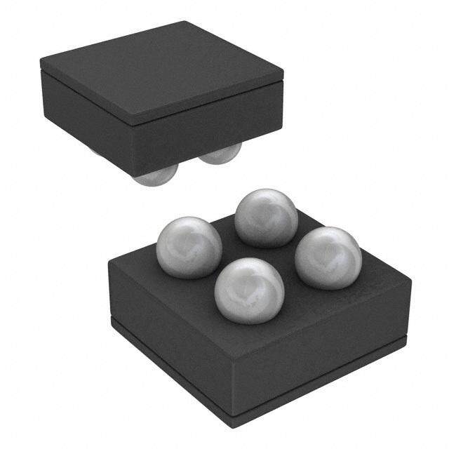
| 描述 | IC DETECTOR RF POWER 6-LLP射频检测器 Sgl Rf Detector W/ LLP |
| 产品分类 | |
| 品牌 | Texas Instruments |
| 产品手册 | |
| 产品图片 |
|
| rohs | 符合RoHS无铅 / 符合限制有害物质指令(RoHS)规范要求 |
| 产品系列 | RF集成电路,射频检测器,Texas Instruments LMV225SD/NOPB- |
| 数据手册 | |
| 产品型号 | LMV225SD/NOPB |
| RF类型 | 手机,CDMA,CDMA2000,EDGE,GSM,GPRS,TDMA,W-CDMA |
| 产品目录页面 | |
| 产品种类 | 射频检测器 |
| 其它名称 | *LMV225SD/NOPB |
| 制造商产品页 | http://www.ti.com/general/docs/suppproductinfo.tsp?distId=10&orderablePartNumber=LMV225SD/NOPB |
| 包装 | 剪切带 (CT) |
| 商标 | Texas Instruments |
| 安装风格 | SMD/SMT |
| 封装 | Reel |
| 封装/外壳 | 6-WDFN 裸露焊盘 |
| 封装/箱体 | WSON-6 |
| 工作电源电压 | 2.7 V to 5.5 V |
| 工厂包装数量 | 1000 |
| 最大工作温度 | + 85 C |
| 最大正向电压 | 2.7 V to 5.5 V |
| 最小工作温度 | - 40 C |
| 标准包装 | 1 |
| 电压-电源 | 2.7 V ~ 5 V |
| 电流-电源 | 8mA |
| 精度 | 1dB |
| 系列 | LMV225 |
| 输入范围 | -30dBm ~ 0dBm |
| 配置 | Single |
| 频率 | 450MHz ~ 2GHz |
| 频率范围 | 450 MHz to 2000 MHz |


- 商务部:美国ITC正式对集成电路等产品启动337调查
- 曝三星4nm工艺存在良率问题 高通将骁龙8 Gen1或转产台积电
- 太阳诱电将投资9.5亿元在常州建新厂生产MLCC 预计2023年完工
- 英特尔发布欧洲新工厂建设计划 深化IDM 2.0 战略
- 台积电先进制程称霸业界 有大客户加持明年业绩稳了
- 达到5530亿美元!SIA预计今年全球半导体销售额将创下新高
- 英特尔拟将自动驾驶子公司Mobileye上市 估值或超500亿美元
- 三星加码芯片和SET,合并消费电子和移动部门,撤换高东真等 CEO
- 三星电子宣布重大人事变动 还合并消费电子和移动部门
- 海关总署:前11个月进口集成电路产品价值2.52万亿元 增长14.8%


PDF Datasheet 数据手册内容提取
LMV225, LMV226, LMV228 www.ti.com SNWS013L–AUGUST2003–REVISEDMARCH2013 LMV225/LMV226/LMV228 RF Power Detector for CDMA and WCDMA CheckforSamples:LMV225,LMV226,LMV228 FEATURES DESCRIPTION 1 • 30dBLinearindBPowerDetectionRange The LMV225/LMV226/LMV228 are 30 dB RF power 2 detectors intended for use in CDMA and WCDMA • OutputVoltageRange0.2to2V applications. The device has an RF frequency range • LogicLowShutdown from 450 MHz to 2 GHz. It provides an accurate • Multi-BandOperationfrom450MHzto2000 temperature and supply compensated output voltage MHz that relates linearly to the RF input power in dBm. The circuit operates with a single supply from 2.7V to • AccurateTemperatureCompensation 5.5V. The LMV225/LMV226/LMV228 have an • Packages: integratedfilterforlow-rippleaveragepowerdetection – DSBGAThin1.0mmx1.0mmx0.6mm of CDMA signals with 30 dB dynamic range. Additional filtering can be applied using a single – DSBGAUltraThin1.0mmx1.0mmx0.35 externalcapacitor. mm The LMV225 has an RF power detection range from – WSON2.2mmx2.5mmx0.8mm –30 dBm to 0 dBm and is ideally suited for direct use – (LMV225andLMV228) in combination with resistive taps. The LMV226/LMV228 have a detection range from –15 APPLICATIONS dBm to 15 dBm and are intended for use in combination with a directional coupler. The LMV226 • CDMARFPowerControl is equipped with a buffered output which makes it • WCDMARFPowerControl suitable for GSM, EDGE, GPRS and TDMA • CDMA2000RFPowerControl applications. • PAModules The device is active for Enable = HI, otherwise it is in a low power consumption shutdown mode. During shutdown the output will be LOW. The output voltage ranges from 0.2V to 2V and can be scaled down to meetADCinputrangerequirements. The LMV225/LMV226/LMV228 power detectors are offered in the thin 1.0 mm x 1.0 mm x 0.6 mm DSBGA package and the ultra thin 1.0 mm x 1.0 mm x 0.35 mm DSBGA package. The LMV225 and the LMV228 are also offered in the 2.2 mm x 2.5 mm x 0.8mmWSONpackage. Typical Application RF ANTENNA PA RF ANTENNA PA R1 1.8 k: VDD C 50: 100 pF VDD LMV225 C RFIN/EN 100 pF R2 OUT LMV226/ ENABLE 10 k: RFIN/EN LMV228 OUT GND ENABLE R2 10 k: GND Figure1.LMV225 Figure2.LMV226/LMV228 1 Pleasebeawarethatanimportantnoticeconcerningavailability,standardwarranty,anduseincriticalapplicationsof TexasInstrumentssemiconductorproductsanddisclaimerstheretoappearsattheendofthisdatasheet. Alltrademarksarethepropertyoftheirrespectiveowners. 2 PRODUCTIONDATAinformationiscurrentasofpublicationdate. Copyright©2003–2013,TexasInstrumentsIncorporated Products conform to specifications per the terms of the Texas Instruments standard warranty. Production processing does not necessarilyincludetestingofallparameters.
LMV225, LMV226, LMV228 SNWS013L–AUGUST2003–REVISEDMARCH2013 www.ti.com Thesedeviceshavelimitedbuilt-inESDprotection.Theleadsshouldbeshortedtogetherorthedeviceplacedinconductivefoam duringstorageorhandlingtopreventelectrostaticdamagetotheMOSgates. ABSOLUTE MAXIMUM RATINGS (1)(2) SupplyVoltage V -GND 6.0VMax DD ESDTolerance (3) HumanBodyModel 2000V MachineModel 200V StorageTemperatureRange −65°Cto150°C JunctionTemperature (4) 150°CMax MountingTemperature,Infraredorconvection(20sec) Tin/Lead 235°C Lead-Free 260°C (1) AbsoluteMaximumRatingsindicatelimitsbeyondwhichdamagetothedevicemayoccur.OperatingRatingsindicateconditionsfor whichthedeviceisintendedtobefunctional,butspecificperformanceisnotspecified.Forspecificationsandthetestconditions,see theElectricalCharacteristics. (2) IfMilitary/Aerospacespecifieddevicesarerequired,pleasecontacttheTexasInstrumentsSalesOffice/Distributorsforavailabilityand specifications. (3) Humanbodymodel:1.5kΩinserieswith100pF.Machinemodel,0Ωinserieswith100pF. (4) ThemaximumpowerdissipationisafunctionofT ,θ andT .Themaximumallowablepowerdissipationatanyambient J(MAX) JA A temperatureisP =(T -T )/θ .AllnumbersapplyforpackagessoldereddirectlyintoaPCboard D J(MAX) A JA OPERATING RATINGS (1) SupplyVoltage 2.7Vto5.5V TemperatureRange −40°Cto+85°C RFFrequencyRange 450MHzto2GHz (1) AbsoluteMaximumRatingsindicatelimitsbeyondwhichdamagetothedevicemayoccur.OperatingRatingsindicateconditionsfor whichthedeviceisintendedtobefunctional,butspecificperformanceisnotspecified.Forspecificationsandthetestconditions,see theElectricalCharacteristics. 2 SubmitDocumentationFeedback Copyright©2003–2013,TexasInstrumentsIncorporated ProductFolderLinks:LMV225 LMV226 LMV228
LMV225, LMV226, LMV228 www.ti.com SNWS013L–AUGUST2003–REVISEDMARCH2013 2.7 DC AND AC ELECTRICAL CHARACTERISTICS Unlessotherwisespecified,alllimitsarespecifiedtoV =2.7V;T =25°C.Boldfacelimitsapplyattemperatureextremes. (1) DD J Symbol Parameter Condition Min Typ Max Units I SupplyCurrent ActiveMode:RF /E =V LMV225 4.8 7 DD IN N DD (DC),NoRFInputPower 8 Present LMV226 4.9 6.2 mA 8 LMV228 4.9 6.2 8 Shutdown:RF /E =GND(DC),NoRFInput 0.44 4.5 μA IN N PowerPresent V E LogicLowInputLevel 0.8 V LOW N (2) V E LogicHighInputLevel 1.8 V HIGH N (2) t Turn-on-Time (3) NoRFInputPowerPresent, LMV225 2.1 on OutputLoadedwith10pF LMV226 1.2 μs LMV228 1.7 t RiseTime (4) StepfromnoPowerto LMV225 4.5 r 0dBmApplied,Output Loadedwith10pF μs StepfromnoPowerto LMV226 1.8 15dBmApplied,Output LMV228 4.8 Loadedwith10pF I CurrentintoRF /E Pin 1 μA EN IN N P InputPowerRange (5) LMV225 −30 dBm IN 0 −43 dBV −13 LMV226 −15 dBm 15 −28 dBV 2 LMV228 −15 dBm 15 −28 dBV 2 (1) ElectricalTablevaluesapplyonlyforfactorytestingconditionsatthetemperatureindicated.Factorytestingconditionsresultinvery limitedself-heatingofthedevicesuchthatT =T .Nospecificationofparametricperformanceisindicatedintheelectricaltablesunder J A conditionsofinternalself-heatingwhereT >T . J A (2) Alllimitsarespecifiedbydesignorstatisticalanalysis (3) Turn-ontimeismeasuredbyconnectinga10kΩresistortotheRF /E pin.Beawarethatintheactualapplicationonthefrontpage, IN N theRC-timeconstantofresistorR andcapacitorCaddsanadditionaldelay. 2 (4) Typicalvaluesrepresentthemostlikelyparametricnorm. (5) PowerindBV=dBm+13whentheimpedanceis50Ω. Copyright©2003–2013,TexasInstrumentsIncorporated SubmitDocumentationFeedback 3 ProductFolderLinks:LMV225 LMV226 LMV228
LMV225, LMV226, LMV228 SNWS013L–AUGUST2003–REVISEDMARCH2013 www.ti.com 2.7 DC AND AC ELECTRICAL CHARACTERISTICS (continued) Unlessotherwisespecified,alllimitsarespecifiedtoV =2.7V;T =25°C.Boldfacelimitsapplyattemperatureextremes.(1) DD J Symbol Parameter Condition Min Typ Max Units LogarithmicSlope (6) 900MHz LMV225 44.0 LMV226 44.5 LMV228 44.0 DSBGA LMV228WSON 48.5 1800MHz LMV225 39.4 LMV226 41.6 LMV228 41.9 DSBGA LMV228WSON 47.4 mV/dB 1900MHz LMV225 38.5 LMV226 41.2 LMV228 41.6 DSBGA LMV228WSON 46.6 2000MHz LMV225 38.5 LMV226 41.0 LMV228 41.2 DSBGA LMV228WSON 45.4 LogarithmicIntercept (6) 900MHz LMV225 −45.5 LMV226 −24.5 LMV228 −27.2 DSBGA LMV228WSON −23.7 1800MHz LMV225 −46.6 LMV226 −25.1 LMV228 −28.2 DSBGA LMV228WSON −23.8 dBm 1900MHz LMV225 −46.3 LMV226 −24.9 LMV228 −28.0 DSBGA LMV228WSON −23.7 2000MHz LMV225 −46.7 LMV226 −24.7 LMV228 −28.0 DSBGA LMV228WSON -23.6 V OutputVoltage NoRFInputPowerPresent LMV225 214 350 OUT LMV226 223 350 mV LMV228 228 350 I OutputCurrentSourcing/Sinking LMV226Only 4.5 5.3 mA OUT R OutputImpedance LMV225/LMV228only,noRFInputPower 19.8 29 kΩ OUT Present 34 (6) Deviceissetinactivemodewitha10kΩresistorfromV toRF /E .RFsignalisappliedusinga50ΩRFsignalgeneratorAC DD IN N coupledtotheRF /E pinusinga100pFcouplingcapacitor. IN N 4 SubmitDocumentationFeedback Copyright©2003–2013,TexasInstrumentsIncorporated ProductFolderLinks:LMV225 LMV226 LMV228
LMV225, LMV226, LMV228 www.ti.com SNWS013L–AUGUST2003–REVISEDMARCH2013 2.7 DC AND AC ELECTRICAL CHARACTERISTICS (continued) Unlessotherwisespecified,alllimitsarespecifiedtoV =2.7V;T =25°C.Boldfacelimitsapplyattemperatureextremes.(1) DD J Symbol Parameter Condition Min Typ Max Units e OutputReferredNoise RFInput=1800MHz,−10dBmforLMV225 700 n and5dBmforLMV226/LMV228,Measuredat nV/√Hz 10kHz VariationDuetoTemperature 900MHz,RF =0dBm LMV225 +0.64 IN Referredto25°C −1.07 900MHz,RF =15dBm LMV226 +0.05 IN Referredto25°C −0.02 LMV228 +0.22 DSBGA −0.36 LMV228WSON +0.87 −0.87 1800MHz,RF =0dBm LMV225 +0.09 IN Referredto25°C −0.86 1800MHz,RF =15dBm LMV226 +0.07 IN Referredto25°C −0.10 LMV228 +0.29 DSBGA −0.57 LMV228WSON +1.04 −1.23 dB 1900MHz,RF =0dBm LMV225 +0 IN Referredto25°C −0.69 1900MHz,RF =15dBm LMV226 +0 IN Referredto25°C −0.10 LMV228 +0.23 DSBGA −0.64 LMV228WSON +1.05 −1.45 2000MHz,RF =0dBm LMV225 +0 IN Referredto25°C −0.86 2000MHz,RF =15dBm LMV226 +0 IN Referredto25°C −0.29 LMV228 +0.27 DSBGA −0.65 LMV228WSON +1.04 −2.02 Copyright©2003–2013,TexasInstrumentsIncorporated SubmitDocumentationFeedback 5 ProductFolderLinks:LMV225 LMV226 LMV228
LMV225, LMV226, LMV228 SNWS013L–AUGUST2003–REVISEDMARCH2013 www.ti.com 5.0 DC AND AC ELECTRICAL CHARACTERISTICS Unlessotherwisespecified,alllimitsarespecifiedtoV =5.0V;T =25°C.Boldfacelimitsapplyattemperatureextremes. (1) DD J Symbol Parameter Condition Min Typ Max Units I SupplyCurrent ActiveMode:RF /E =V LMV225 5.3 7.5 DD IN N DD (DC),noRFInputPower 9 Present. LMV226 5.3 6.8 mA 9 LMV228 5.4 6.8 9 Shutdown:RF /E =GND(DC),noRFInput 0.32 4.5 μA IN N PowerPresent. V E LogicLowInputLevel 0.8 V LOW N (2) V E LogicHighInputLevel 1.8 V HIGH N (2) t Turn-on-Time (3) NoRFInputPowerPresent, LMV225 2.1 on OutputLoadedwith10pF LMV226 1.0 μs LMV228 1.7 t RiseTime (4) StepfromnoPowerto LMV225 4.5 r 0dBmApplied,Output Loadedwith10pF μs StepfromnoPowerto LMV226 1.4 15dBmApplied,Output LMV228 4.8 Loadedwith10pF I CurrentIntoRF /E Pin 1 μA EN IN N P InputPowerRange (5) LMV225 −30 dBm IN 0 −43 dBV −13 LMV226 −15 dBm 15 −28 dBV 2 LMV228 −15 dBm 15 −28 dBV 2 (1) ElectricalTablevaluesapplyonlyforfactorytestingconditionsatthetemperatureindicated.Factorytestingconditionsresultinvery limitedself-heatingofthedevicesuchthatT =T .Nospecificationofparametricperformanceisindicatedintheelectricaltablesunder J A conditionsofinternalself-heatingwhereT >T . J A (2) Alllimitsarespecifiedbydesignorstatisticalanalysis (3) Turn-ontimeismeasuredbyconnectinga10kΩresistortotheRF /E pin.Beawarethatintheactualapplicationonthefrontpage, IN N theRC-timeconstantofresistorR andcapacitorCaddsanadditionaldelay. 2 (4) Typicalvaluesrepresentthemostlikelyparametricnorm. (5) PowerindBV=dBm+13whentheimpedanceis50Ω. 6 SubmitDocumentationFeedback Copyright©2003–2013,TexasInstrumentsIncorporated ProductFolderLinks:LMV225 LMV226 LMV228
LMV225, LMV226, LMV228 www.ti.com SNWS013L–AUGUST2003–REVISEDMARCH2013 5.0 DC AND AC ELECTRICAL CHARACTERISTICS (continued) Unlessotherwisespecified,alllimitsarespecifiedtoV =5.0V;T =25°C.Boldfacelimitsapplyattemperatureextremes.(1) DD J Symbol Parameter Condition Min Typ Max Units LogarithmicSlope (6) 900MHz LMV225 44.6 LMV226 44.6 LMV228 44.2 DSBGA LMV228WSON 48.4 1800MHz LMV225 40.6 LMV226 42.2 LMV228 42.4 DSBGA LMV228WSON 48.3 mV/dB 1900MHz LMV225 39.6 LMV226 41.8 LMV228 42.2 DSBGA LMV228WSON 47.8 2000MHz LMV225 39.7 LMV226 41.6 LMV228 41.8 DSBGA LMV228WSON 47.2 LogarithmicIntercept (6) 900MHz LMV225 −47.0 LMV226 −25.0 LMV228 −27.7 DSBGA LMV228WSON −23.9 1800MHz LMV225 −48.5 LMV226 −25.7 LMV228 −28.9 DSBGA LMV228WSON −23.6 dBm 1900MHz LMV225 −48.2 LMV226 −25.6 LMV228 −28.7 DSBGA LMV228WSON −23.1 2000MHz LMV225 −48.9 LMV226 −25.5 LMV228 −28.7 DSBGA LMV228WSON −23.0 V OutputVoltage NoRFInputPowerPresent LMV225 222 400 OUT LMV226 231 400 mV LMV228 244 400 I OutputCurrentSourcing/Sinking LMV226Only 4.5 5.3 mA OUT R OutputImpedance NoRFInputPowerPresent 23.7 29 kΩ OUT 31 (6) Deviceissetinactivemodewitha10kΩresistorfromV toRF /E .RFsignalisappliedusinga50ΩRFsignalgeneratorAC DD IN N coupledtotheRF /E pinusinga100pFcouplingcapacitor. IN N Copyright©2003–2013,TexasInstrumentsIncorporated SubmitDocumentationFeedback 7 ProductFolderLinks:LMV225 LMV226 LMV228
LMV225, LMV226, LMV228 SNWS013L–AUGUST2003–REVISEDMARCH2013 www.ti.com 5.0 DC AND AC ELECTRICAL CHARACTERISTICS (continued) Unlessotherwisespecified,alllimitsarespecifiedtoV =5.0V;T =25°C.Boldfacelimitsapplyattemperatureextremes.(1) DD J Symbol Parameter Condition Min Typ Max Units e OutputReferredNoise RFInput=1800MHz,−10dBmforLMV225 700 nV/√Hz n and5dBmforLMV226/LMV228,Measuredat 10kHz VariationDuetoTemperature 900MHz,RF =0dBm LMV225 +0.89 IN Referredto25°C −1.16 900MHz,RF =15dBm LMV226 +0.25 IN Referredto25°C −0.16 LMV228 +0.46 DSBGA −0.62 LMV228WSON +1.39 −1.19 1800MHz,RF =0dBm LMV225 +0.3 IN Referredto25°C −0.82 1800MHz,RF =15dBm LMV226 +0.21 IN Referredto25°C −0.09 LMV228 +0.55 DSBGA −0.78 LMV228WSON +1.39 −1.43 dB 1900MHz,RF =0dBm LMV225 +0.34 IN Referredto25°C −0.63 1900MHz,RF =15dBm LMV226 +0.21 IN Referredto25°C −0.19 LMV228 +0.55 DSBGA −0.93 LMV228WSON +1.54 −1.64 2000MHz,RF =0dBm LMV225 +0.22 IN Referredto25°C −0.75 2000MHzRF =15dBm LMV226 +0.25 IN Referredto25°C −0.34 LMV228 +0.61− DSBGA 0.91 LMV228WSON +0.89 −0.99 8 SubmitDocumentationFeedback Copyright©2003–2013,TexasInstrumentsIncorporated ProductFolderLinks:LMV225 LMV226 LMV228
LMV225, LMV226, LMV228 www.ti.com SNWS013L–AUGUST2003–REVISEDMARCH2013 CONNECTION DIAGRAM GND 1 6 OUT RFIN/EN A1 A2 VDD NC 2 5 NC 1.0mm RFIN/EN 3 4 VDD GND B1 B2 OUT 1.0mm BUMP PITCH 500Pm BUMP DIAMETER 300Pm SOLDER DOT DIAMETER/ 125Pm PASSIVATION OPENING Figure3.4-BumpDSBGA–TopView Figure4. 6-pinWSON–TopView SeePackageNumberYZR0004orYPD0004 SeePackageNumberNGF0006A PINDESCRIPTIONS Pin Name Description DSBGA WSON6 PowerSupply A2 4 V PositiveSupplyVoltage DD B1 1 GND PowerGround A1 3 RF /E DCvoltagedeterminesenablestateofthedevice(HIGH= IN N deviceactive).ACvoltageistheRFinputsignaltothe detector(beyond450MHz).TheRF /E pinisinternally IN N terminatedwith50Ωinserieswith45pF. Output B2 6 Out Groundreferenceddetectoroutputvoltage(linearindBm) Copyright©2003–2013,TexasInstrumentsIncorporated SubmitDocumentationFeedback 9 ProductFolderLinks:LMV225 LMV226 LMV228
LMV225, LMV226, LMV228 SNWS013L–AUGUST2003–REVISEDMARCH2013 www.ti.com Block Diagrams VDD LOGIC ENABLE DETECTOR OUT I / I RFIN/EN 10 dB 10 dB 10 dB GND Figure5. LMV225 VDD LOGIC ENABLE I / I + OUT - RFIN/EN 10 dB 10 dB 10 dB GND Figure6. LMV226 10 SubmitDocumentationFeedback Copyright©2003–2013,TexasInstrumentsIncorporated ProductFolderLinks:LMV225 LMV226 LMV228
LMV225, LMV226, LMV228 www.ti.com SNWS013L–AUGUST2003–REVISEDMARCH2013 VDD LOGIC ENABLE OUT I / I RFIN/EN 10 dB 10 dB 10 dB GND Figure7. LMV228 Copyright©2003–2013,TexasInstrumentsIncorporated SubmitDocumentationFeedback 11 ProductFolderLinks:LMV225 LMV226 LMV228
LMV225, LMV226, LMV228 SNWS013L–AUGUST2003–REVISEDMARCH2013 www.ti.com TYPICAL PERFORMANCE CHARACTERISTICS LMV225 Unlessotherwisespecified,V =2.7V,T =25°C. DD J SupplyCurrent OutputVoltage vs. vs. SupplyVoltage(LMV225) RFInputPower(LMV225) 8 2.50 2.25 900MHz 7.5 85°C 2.00 )A 7 1800MHz m 1.75 ( TNE 6.5 )V 1.50 1900MHz 2000MHz RRUC Y 5.56 25°C ( VTUO 11..0205 L P 0.75 P U 5 S -40°C 0.50 4.5 0.25 4 0.00 2.5 3 3.5 4 4.5 5 -50 -40 -30 -20 -10 0 10 20 SUPPLY VOLTAGE (V) RF INPUT POWER (dBm) Figure8. Figure9. OutputVoltageandLogConformancevs. OutputVoltageandLogConformancevs. RFInputPower@900MHz(LMV225) RFInputPower@1800MHz(LMV225) 2.50 5 2.50 5 85°C 85°C 2.25 85°C 25°C 4 2.25 85°C 25°C 4 2.00 3 2.00 3 25°C 1.75 2 1.75 25°C 2 )V(TUO 11..2550 -40°C -40°C 10 )Bd(ROR )V(TUO 11..2550 -40°C -40°C 10 )Bd( ROR V 1.00 -1 R V 1.00 -1 R E E 0.75 -2 0.75 -2 0.50 -3 0.50 -3 0.25 -4 0.25 -4 0.00 -5 0.00 -5 -50 -40 -30 -20 -10 0 10 20 -50 -40 -30 -20 -10 0 10 20 RF INPUTPOWER (dBm) RF INPUTPOWER (dBm) Figure10. Figure11. OutputVoltageandLogConformance vs. OutputVoltageandLogConformancevs. RFInputPower@1900MHz(LMV225) RFInputPower@2000MHz(LMV225) 2.50 5 2.50 5 85°C 85°C 2.25 25°C 4 2.25 25°C 4 85°C 85°C 2.00 3 2.00 3 25°C 25°C 1.75 2 1.75 2 )V(TUO 11..2550 -40°C 10 )Bd( ROR )V(TUO 11..2550 -40°C 10 )Bd(ROR V 1.00 -40°C -1 RE V 1.00 -40°C -1 RE 0.75 -2 0.75 -2 0.50 -3 0.50 -3 0.25 -4 0.25 -4 0.00 -5 0.00 -5 -50 -40 -30 -20 -10 0 10 20 -50 -40 -30 -20 -10 0 10 20 RF INPUTPOWER (dBm) RF INPUTPOWER (dBm) Figure12. Figure13. 12 SubmitDocumentationFeedback Copyright©2003–2013,TexasInstrumentsIncorporated ProductFolderLinks:LMV225 LMV226 LMV228
LMV225, LMV226, LMV228 www.ti.com SNWS013L–AUGUST2003–REVISEDMARCH2013 TYPICAL PERFORMANCE CHARACTERISTICS LMV225 (continued) Unlessotherwisespecified,V =2.7V,T =25°C. DD J LogarithmicSlopevs.Frequency(LMV225) LogarithmicInterceptvs.Frequency(LMV225) 47 -43 46 -40°C 45 -44 )B 44 25°C )m -40°C d/Vm( EPOLS 44443012 85°C Bd( TPECRET --4465 25°C N I 39 -47 38 85°C 37 -48 400 800 1200 1600 2000 400 800 1200 1600 2000 FREQUENCY (MHz) FREQUENCY (MHz) Figure14. Figure15. OutputVariationvs.RFInputPower OutputVariationvs.RFInputPower Normalizedto25°C@900MHz(LMV225) Normalizedto25°C@1800MHz(LMV225) 1.5 1.5 1.0 85°C 1.0 85°C 0.5 0.5 OR (dB) 0.0 OR (dB) 0.0 R R R R E -0.5 E -0.5 -40°C -1.0 -1.0 -40°C -1.5 -1.5 -50 -40 -30 -20 -10 0 10 20 -50 -40 -30 -20 -10 0 10 20 RF INPUT POWER (dBm) RF INPUT POWER (dBm) Figure16. Figure17. OutputVariationvs.RFInputPower OutputVariationvs.RFInputPower Normalizedto25°C@1900MHz(LMV225) Normalizedto25°C@2000MHz(LMV225) 1.5 1.5 85°C 85°C 1.0 1.0 0.5 0.5 B) B) d d OR ( 0.0 OR ( 0.0 R R R R E E -0.5 -0.5 -1.0 -1.0 -40°C -40°C -1.5 -1.5 -50 -40 -30 -20 -10 0 10 20 -50 -40 -30 -20 -10 0 10 20 RF INPUT POWER (dBm) RF INPUT POWER (dBm) Figure18. Figure19. Copyright©2003–2013,TexasInstrumentsIncorporated SubmitDocumentationFeedback 13 ProductFolderLinks:LMV225 LMV226 LMV228
LMV225, LMV226, LMV228 SNWS013L–AUGUST2003–REVISEDMARCH2013 www.ti.com TYPICAL PERFORMANCE CHARACTERISTICS LMV225 (continued) Unlessotherwisespecified,V =2.7V,T =25°C. DD J PSRRvs.Frequency PSRRvs.Frequency (LMV225inDSBGA) (LMV225inWSON) 70 5V 60 50 )Bd 40 ( R 2.7V R S 30 P 20 10 0 100 1k 10k 100k 1M FREQUENCY (Hz) Figure20. Figure21. RFInputImpedancevs.Frequency@Resistanceand RFInputImpedancevs.Frequency@Resistanceand Reactance(LMV225inDSBGA) Reactance(LMV225inWSON) 150 100 R :) ( E 50 C N A D E 0 P M I X -50 -100 0.4 0.6 0.8 1.0 1.2 1.4 1.6 1.8 2.0 FREQUENCY (GHz) Figure22. Figure23. TYPICAL PERFORMANCE CHARACTERISTICS LMV226 Unlessotherwisespecified,V =2.7V,T=25°C. DD J SupplyCurrentvs.SupplyVoltage(LMV226) OutputVoltagevs.RFInputPower(LMV226) 7.0 2.50 6.5 2.25 900 MHz )Am 6.0 85°C 2.00 1800 MHz ( T 5.5 1.75 NERRU 5.0 25°C )V( TU 11..2550 1900 MHz C 4.5 O Y V 1.00 2000 MHz LPP 4.0 0.75 US 3.5 -40°C 0.50 3.0 0.25 2.5 0.00 2.5 3 3.5 4 4.5 5 -50 -40 -30 -20 -10 0 10 20 SUPPLY VOLTAGE (V) RF INPUT POWER (dBm) Figure24. Figure25. 14 SubmitDocumentationFeedback Copyright©2003–2013,TexasInstrumentsIncorporated ProductFolderLinks:LMV225 LMV226 LMV228
LMV225, LMV226, LMV228 www.ti.com SNWS013L–AUGUST2003–REVISEDMARCH2013 TYPICAL PERFORMANCE CHARACTERISTICS LMV226 (continued) Unlessotherwisespecified,V =2.7V,T=25°C. DD J OutputVoltageandLogConformancevs. OutputVoltageandLogConformancevs.RFInputPower RFInputPower@900MHz(LMV226) @1800MHz(LMV226) 2.50 5 2.50 5 2.25 4 2.25 4 2.00 85°C 3 2.00 85°C 85°C 3 25°C 25°C 1.75 2 1.75 2 )V( TUO 11..5205 852°5C°-C40°C -40°C 10 )Bd( ROR )V( TUO 11..5205 25°C-40°C -40°C 10 B)d( ROR V 1.00 -1 RE V 1.00 -1 RE 0.75 -2 0.75 -2 0.50 -3 0.50 -3 0.25 -4 0.25 -4 0.00 -5 0.00 -5 -50 -40 -30 -20 -10 0 10 20 -50 -40 -30 -20 -10 0 10 20 RF INPUT POWER (dBm) RF INPUT POWER (dBm) Figure26. Figure27. OutputVoltageandLogConformancevs.RFInputPower OutputVoltageandLogConformancevs.RFInputPower @1900MHz(LMV226) @2000MHz(LMV226) 2.50 5 2.50 5 2.25 4 2.25 4 2.00 85°C 85°C 3 2.00 85°C 85°C 3 25°C 25°C 1.75 2 1.75 2 )V( TUO 11..5205 25-°4C0°C -40°C 10 )Bd( ROR )V( TUO 11..5205 25°C -40°C -40°C 10 )Bd( ROR V 1.00 -1 R V 1.00 -1 R E E 0.75 -2 0.75 -2 0.50 -3 0.50 -3 0.25 -4 0.25 -4 0.00 -5 0.00 -5 -50 -40 -30 -20 -10 0 10 20 -50 -40 -30 -20 -10 0 10 20 RF INPUT POWER (dBm) RF INPUT POWER (dBm) Figure28. Figure29. LogarithmicSlopevs.Frequency(LMV226) LogarithmicInterceptvs.Frequency(LMV226) 46 -23.0 -40°C 25°C 45 -23.5 -40°C )Bd/Vm( EPOLS 44441234 85°C )mBd( TPECRETNI ----22225544....5050 25°C 85°C 40 -26.0 39 -26.5 400 800 1200 1600 2000 400 800 1200 1600 2000 FREQUENCY (MHz) FREQUENCY (MHz) Figure30. Figure31. Copyright©2003–2013,TexasInstrumentsIncorporated SubmitDocumentationFeedback 15 ProductFolderLinks:LMV225 LMV226 LMV228
LMV225, LMV226, LMV228 SNWS013L–AUGUST2003–REVISEDMARCH2013 www.ti.com TYPICAL PERFORMANCE CHARACTERISTICS LMV226 (continued) Unlessotherwisespecified,V =2.7V,T=25°C. DD J OutputVariationvs.RFInputPower OutputVariationvs.RFInputPower Normalizedto25°C@900MHz(LMV226) Normalizedto25°C@1800MHz(LMV226) 1.5 1.5 1.0 85°C 1.0 85°C 0.5 0.5 )B )B d d ( R 0.0 ( R 0.0 O O R R R R E -0.5 -40°C E -0.5 -40°C -1.0 -1.0 -1.5 -1.5 -50 -40 -30 -20 -10 0 10 20 -50 -40 -30 -20 -10 0 10 20 RF INPUT POWER (dBm) RF INPUT POWER (dBm) Figure32. Figure33. OutputVariationvs.RFInputPower OutputVariationvs.RFInputPower Normalizedto25°C@1900MHz(LMV226) Normalizedto25°C@2000MHz(LMV226) 1.5 1.5 1.0 85°C 1.0 85°C 0.5 0.5 dB) )B OR ( 0.0 d( R 0.0 R O R R E -0.5 RE -0.5 -40°C -1.0 -40°C -1.0 -1.5 -1.5 -50 -40 -30 -20 -10 0 10 20 -50 -40 -30 -20 -10 0 10 20 RF INPUT POWER (dBm) RF INPUT POWER (dBm) Figure34. Figure35. PSRRvs.Frequency RFInputImpedancevs.Frequency@Resistanceand (LMV226) Reactance(LMV226) 70 150 5V 60 100 50 R :) )Bd( RRSP 3400 2.7V ( ECNADEP 500 M 20 I X -50 10 0 -100 100 1k 10k 100k 1M 0.4 0.6 0.8 1.0 1.2 1.4 1.6 1.8 2.0 FREQUENCY (Hz) FREQUENCY (GHz) Figure36. Figure37. 16 SubmitDocumentationFeedback Copyright©2003–2013,TexasInstrumentsIncorporated ProductFolderLinks:LMV225 LMV226 LMV228
LMV225, LMV226, LMV228 www.ti.com SNWS013L–AUGUST2003–REVISEDMARCH2013 TYPICAL PERFORMANCE CHARACTERISTICS LMV228 IN DSBGA Unlessotherwisespecified,V =2.7V,T=25°C. DD J SupplyCurrentvs.SupplyVoltage OutputVoltagevs.RFInputPower (LMV228inDSBGA) (LMV228inDSBGA) 7.0 2.50 6.5 2.25 900 MHz )Am 6.0 85°C 2.00 1800 MHz (TN 5.5 1.75 1900 MHz ER 5.0 )V 1.50 RUC 4.5 25°C ( TUO 1.25 2000 MHz Y V 1.00 LP 4.0 P 0.75 U S 3.5 -40°C 0.50 3.0 0.25 2.5 0.00 2.5 3 3.5 4 4.5 5 -50 -40 -30 -20 -10 0 10 20 SUPPLYVOLTAGE (V) RF INPUT POWER (dBm) Figure38. Figure39. OutputVoltageandLogConformancevs. OutputVoltageandLogConformancevs. RFInputPower@900MHz(LMV228inDSBGA) RFInputPower@1800MHz(LMV228inDSBGA) 2.50 5 2.50 5 2.25 85°C 4 2.25 85°C 4 25°C 25°C 2.00 3 2.00 3 85°C 1.75 2 1.75 2 )V( TUO 11..5205 852°5C°-C40°C -40°C 10 )Bd( ROR )V( TUO 11..5205 25°C-40°C -40°C 10 )Bd( ROR V 1.00 -1 R V 1.00 -1 R E E 0.75 -2 0.75 -2 0.50 -3 0.50 -3 0.25 -4 0.25 -4 0.00 -5 0.00 -5 -50 -40 -30 -20 -10 0 10 20 -50 -40 -30 -20 -10 0 10 20 RF INPUT POWER (dBm) RF INPUT POWER (dBm) Figure40. Figure41. OutputVoltageandLogConformancevs. OutputVoltageandLogConformancevs. RFInputPower@1900MHz(LMV228inDSBGA) RFInputPower@2000MHz(LMV228inDSBGA) 2.50 5 2.50 5 2.25 85°C 4 2.25 85°C 4 25°C 2.00 3 2.00 25°C 3 85°C 85°C 1.75 2 1.75 2 )V( TUO 11..5205 25°C-40°C -40°C 10 )Bd( ROR )V( TUO 11..5205 25°C-40°C -40°C 10 B)d( ROR V 1.00 -1 R V 1.00 -1 R E E 0.75 -2 0.75 -2 0.50 -3 0.50 -3 0.25 -4 0.25 -4 0.00 -5 0.00 -5 -50 -40 -30 -20 -10 0 10 20 -50 -40 -30 -20 -10 0 10 20 RF INPUT POWER (dBm) RF INPUT POWER (dBm) Figure42. Figure43. Copyright©2003–2013,TexasInstrumentsIncorporated SubmitDocumentationFeedback 17 ProductFolderLinks:LMV225 LMV226 LMV228
LMV225, LMV226, LMV228 SNWS013L–AUGUST2003–REVISEDMARCH2013 www.ti.com TYPICAL PERFORMANCE CHARACTERISTICS LMV228 IN DSBGA (continued) Unlessotherwisespecified,V =2.7V,T=25°C. DD J LogarithmicSlopevs. LogarithmicInterceptvs. Frequency(LMV228inDSBGA) Frequency(LMV228inDSBGA) 44.5 -25.5 -40°C 25°C 44.0 -26.0 -40°C 43.5 )Bd/Vm( EPOLS 44441223....5050 85°C )mBd( TPECRETNI ----22228776....0505 85°C 25°C 41.0 -28.5 40.5 -29.0 400 800 1200 1600 2000 400 800 1200 1600 2000 FREQUENCY (MHz) FREQUENCY (MHz) Figure44. Figure45. OutputVariationvs. OutputVariationvs. RFInputPowerNormalizedto25°C@900MHz(LMV228in RFInputPowerNormalizedto25°C@1800MHz(LMV228in DSBGA) DSBGA) 1.5 1.5 1.0 85°C 1.0 85°C 0.5 0.5 )B )B d d ( R 0.0 ( R 0.0 O O R R R R E -0.5 -40°C E -0.5 -40°C -1.0 -1.0 -1.5 -1.5 -50 -40 -30 -20 -10 0 10 20 -50 -40 -30 -20 -10 0 10 20 RF INPUT POWER (dBm) RF INPUT POWER (dBm) Figure46. Figure47. OutputVariationvs. OutputVariationvs. RFInputPowerNormalizedto25°C@1900MHz(LMV228in RFInputPowerNormalizedto25°C@2000MHz(LMV228in DSBGA) DSBGA) 1.5 1.5 1.0 1.0 85°C 85°C 0.5 0.5 )B )B d d ( R 0.0 ( R 0.0 O O R R R R E -0.5 E -0.5 -1.0 -40°C -1.0 -40°C -1.5 -1.5 -50 -40 -30 -20 -10 0 10 20 -50 -40 -30 -20 -10 0 10 20 RF INPUT POWER (dBm) RF INPUT POWER (dBm) Figure48. Figure49. 18 SubmitDocumentationFeedback Copyright©2003–2013,TexasInstrumentsIncorporated ProductFolderLinks:LMV225 LMV226 LMV228
LMV225, LMV226, LMV228 www.ti.com SNWS013L–AUGUST2003–REVISEDMARCH2013 TYPICAL PERFORMANCE CHARACTERISTICS LMV228 IN DSBGA (continued) Unlessotherwisespecified,V =2.7V,T=25°C. DD J PSRRvs.Frequency RFInputImpedancevs.Frequency@Resistanceand (LMV228inDSBGA) Reactance(LMV228inDSBGA) 70 150 5V 60 100 50 R :) )Bd( RRSP 3400 2.7V ( ECNADEP 500 M 20 I X -50 10 0 -100 100 1k 10k 100k 1M 0.4 0.6 0.8 1.0 1.2 1.4 1.6 1.8 2.0 FREQUENCY (Hz) FREQUENCY (GHz) Figure50. Figure51. TYPICAL PERFORMANCE CHARACTERISTICS LMV228 IN WSON Unlessotherwisespecified,V =2.7V,T=25°C. DD J SupplyCurrent OutputVoltage vs. vs. SupplyVoltage(LMV228inWSON) RFInputPower(LMV228inWSON) 7.0 6.5 )A 6.0 m 85°C (T 5.5 N E R 5.0 R UC 4.5 25°C Y LP 4.0 P U S 3.5 -40°C 3.0 2.5 2.5 3 3.5 4 4.5 5 SUPPLYVOLTAGE (V) Figure52. Figure53. OutputVoltageandLogConformance vs. OutputVoltageandLogConformancevs. RFInputPower@900MHz(LMV228inWSON) RFInputPower@1800MHz(LMV228inWSON) 2.00 5 2.00 5 1.80 4 1.80 4 85°C 1.60 85°C 3 1.60 3 1.40 2 1.40 2 B) B) (V)T 11..2000 10 OR (d (V)T 11..2000 25°C 10 OR (d VOU 0.80 25°C -1 ERR VOU 0.80 -40°C -1 ERR -40°C 0.60 -2 0.60 -2 85°C 85°C 0.40 -3 0.40 -3 -40°C -40°C 0.20 -4 0.20 -4 25°C 25°C 0.00 -5 0.00 -5 -50 -40 -30 -20 -10 0 10 20 -50 -40 -30 -20 -10 0 10 20 RF INPUTPOWER (dBm) RF INPUTPOWER (dBm) Figure54. Figure55. Copyright©2003–2013,TexasInstrumentsIncorporated SubmitDocumentationFeedback 19 ProductFolderLinks:LMV225 LMV226 LMV228
LMV225, LMV226, LMV228 SNWS013L–AUGUST2003–REVISEDMARCH2013 www.ti.com TYPICAL PERFORMANCE CHARACTERISTICS LMV228 IN WSON (continued) Unlessotherwisespecified,V =2.7V,T=25°C. DD J OutputVoltageandLogConformance vs. OutputVoltageandLogConformancevs. RFInputPower@1900MHz(LMV228inWSON) RFInputPower@2000MHz(LMV228inWSON) 2.00 5 2.00 5 1.80 4 1.80 4 85°C 1.60 3 1.60 3 85°C 1.40 2 1.40 2 B) B) (V)T 11..2000 25°C 10 OR (d (V)T 11..2000 10 OR (d VOU 0.80 -40°C -1 ERR VOU 0.80 25°C -1 ERR -40°C 0.60 -2 0.60 -2 85°C 85°C 0.40 -3 0.40 -3 -40°C -40°C 0.20 -4 0.20 -4 25°C 25°C 0.00 -5 0.00 -5 -50 -40 -30 -20 -10 0 10 20 -50 -40 -30 -20 -10 0 10 20 RF INPUTPOWER (dBm) RF INPUTPOWER (dBm) Figure56. Figure57. LogarithmicSlope LogarithmicIntercept vs. vs. Frequency(LMV228inWSON) Frequency(LMV228inWSON) Figure58. Figure59. OutputVariation OutputVariation vs. vs. RFInputPowerNormalizedto25°C@900MHz(LMV228in RFInputPowerNormalizedto25°C@1800MHz(LMV228in WSON) WSON) Figure60. Figure61. 20 SubmitDocumentationFeedback Copyright©2003–2013,TexasInstrumentsIncorporated ProductFolderLinks:LMV225 LMV226 LMV228
LMV225, LMV226, LMV228 www.ti.com SNWS013L–AUGUST2003–REVISEDMARCH2013 TYPICAL PERFORMANCE CHARACTERISTICS LMV228 IN WSON (continued) Unlessotherwisespecified,V =2.7V,T=25°C. DD J OutputVariation OutputVariation vs. vs. RFInputPowerNormalizedto25°C@1900MHz(LMV228in RFInputPowerNormalizedto25°C@2000MHz(LMV228in WSON) WSON) Figure62. Figure63. PSRR vs. RFInputImpedance Frequency vs. (LMV228inWSON) Frequency@ResistanceandReactance(LMV228inWSON) Figure64. Figure65. Copyright©2003–2013,TexasInstrumentsIncorporated SubmitDocumentationFeedback 21 ProductFolderLinks:LMV225 LMV226 LMV228
LMV225, LMV226, LMV228 SNWS013L–AUGUST2003–REVISEDMARCH2013 www.ti.com APPLICATION NOTES CONFIGURING A TYPICAL APPLICATION The LMV225/LMV226/LMV228 are power detectors intended for CDMA and WCDMA applications. Power applied at its input translates to a DC voltage on the output through a linear-in-dB response. The LMV225 detector is especially suited for power measurements via a high-resistive tap, while the LMV226/LMV228 are designed to be used in combination with a directional coupler. The LMV226 has an additional output voltage bufferandthereforealowoutputimpedance.Thekeyfeaturesofthedevicesareshownin. Table1. DEVICECHARACTERISTICS InputRange(dBm) OutputBuffer Application LMV225 −30/0 No HighResistiveTap LMV226 −15/15 Yes DirectionalCoupler LMV228 −15/15 No DirectionalCoupler In order to match the output power range of the power amplifier (PA) with the range of the LMV225’s input, the high resistive tap needs to be configured correctly. In case of the LMV226/LMV228 the coupling factor of the directionalcouplerneedstobechosencorrectly. HIGH RESISTIVE TAP APPLICATION The constant input impedance of the device enables the realization of a frequency independent input attenuation to adjust the LMV225’s range to the range of the PA. Resistor R and the 50Ω input resistance (R ) of the 1 IN device realize this attenuation (Figure 66). To minimize insertion loss, resistor R needs to be sufficiently large. 1 ThefollowingexampledemonstrateshowtodeterminethepropervalueforR . 1 RF ANTENNA PA R1 1.8 k: 100 pCF RFIN/EN VDD LMV225 RIN OUT R2 CIN 10 k: ENABLE GND Figure66. TypicalLMV225ApplicationwithHighResistiveTap Suppose the useful output power of the PA ranges up to +31 dBm. As the LMV225 can handle input power levels up to 0 dBm. R should realize a minimum attenuation of 31 - 0 = 31 dB. The attenuation realized by R 1 1 andtheeffectiveinputresistanceR ofthedetectorequals: IN R1 AdB = 20·LOG 1+ = 31dB RIN (1) SolvingthisexpressionforR ,usingthatR =50Ω,yields: 1 IN AdB 31 R1 = 1020 -1 · RIN = 1020 -1 · 50 = 1724: (2) InFigure66,R issetto1800Ωresultinginanattenuationof31.4dB. 1 22 SubmitDocumentationFeedback Copyright©2003–2013,TexasInstrumentsIncorporated ProductFolderLinks:LMV225 LMV226 LMV228
LMV225, LMV226, LMV228 www.ti.com SNWS013L–AUGUST2003–REVISEDMARCH2013 DIRECTIONAL COUPLER APPLICATION The LMV226/LMV228 also has a 50Ω input resistance. However, its input range differs compared to the LMV225,i.e.−15dBmto+15dBm.Ifatypicalattenuationofadirectionalcoupleris20dB,theLMV226/LMV228 can be directly connected via the directional coupler to the PA without the need of additional external attenuator (Figure67).DifferentPArangescanbeconfiguredusingcouplerswithothercouplingfactors. RF ANTENNA PA 50: VDD C 100 pF LMV226/ RFIN/EN LMV228 OUT ENABLE R2 10 k: GND Figure67. TypicalLMV226/LMV228Applicationwith DirectionalCoupler SHUTDOWN FUNCTIONALITY TheLMV225/LMV226/LMV228RF /E pinshave2functionscombined: IN N • Enable/Shutdown • Powerinput The capacitor C and the resistor R (Figure 66 and Figure 67) separate the DC shutdown functionality from the 2 AC power measurement. The device is active when Enable = HI, otherwise it is in a low power consumption shutdownmode.DuringshutdowntheoutputwillbeLOW. Capacitor C should be chosen sufficiently large to ensure a corner frequency far below the lowest input frequencytobemeasured.IncaseoftheLMV225thecornerfrequencycanbecalculatedusing: 1 f = C · CIN 2 S (R1 + RIN) C + CIN where • R =50Ω,C =45pFtypical (3) IN IN With R = 1800Ω and C = 100 pF, this results in a corner frequency of 2.8 MHz. This corner frequency is an 1 indicativenumber.Thegoalistohaveamagnitudetransfer,whichissufficientlyflatintheusedfrequencyrange; capacitor C should be chosen significantly larger than capacitor C to assure a proper performance of the high IN resistive tap. Capacitor C shouldn’t be chosen excessively large since the RC-time, it introduces in combination withresistorR ,addstotheturn-ontimeofthedevice. 2 The LMV226/LMV228 do not use a resistor R like the LMV225. Though a resistor is seen on the coupler side 1 (R ). Therefore a similar equation holds for the LMV226/LMV228 LF corner frequency, where R is COUPLER 1 replacedwiththecoupleroutputimpedance(R ). COUPLER WithR =50Ω andC=100pF,theresultingcornerfrequencyis50MHz. COUPLER The output voltage is proportional to the logarithm of the input power, often called “linear-in-dB”. Figure 68shows thetypicaloutputvoltageversusPAoutputpoweroftheLMV225setupasdepictedinFigure66. Copyright©2003–2013,TexasInstrumentsIncorporated SubmitDocumentationFeedback 23 ProductFolderLinks:LMV225 LMV226 LMV228
LMV225, LMV226, LMV228 SNWS013L–AUGUST2003–REVISEDMARCH2013 www.ti.com 2.25 LMV225 2.00 )V RF INPUT POWER ( E 1.75 G 31.4 dB A T 1.50 L O V 1.25 T U P 1.00 T U O 0.75 5 2 2V 0.50 M L 0.25 PA OUTPUT POWER 0.00 -50 -40 -30 -20 -10 0 10 20 30 40 POWER (dBm) Figure68. Typicalpowerdetectorresponse,V vs.PAoutputPower OUT OUTPUT RIPPLE DUE TO AM MODULATION A CDMA modulated carrier wave generally contains some amplitude modulation that might disturb the RF power measurement used for controlling the PA. This section explains the relation between amplitude modulation in the RF signal and the ripple on the output of the LMV225/LMV228. Expressions are provided to estimate this ripple on the output. The ripple can be further reduced by lowpass filtering at the output. This is realized by connecting ancapacitorfromtheoutputoftheLMV225/LMV228toground. EstimatingOutputRipple TheCDMAmodulatedRFinputsignalofFigure68canbedescribedas: V (t)=V [1+μ(t)]cos(2· π· f· t) IN IN where • V istheamplitudeofthecarrierfrequency IN • Amplitudemodulationμ(t)canbebetween-1and1 (4) VIN (1 + P(cid:12) VIN VIN (1 - P(cid:12) 0 Figure69. AMModulatedRFSignal 24 SubmitDocumentationFeedback Copyright©2003–2013,TexasInstrumentsIncorporated ProductFolderLinks:LMV225 LMV226 LMV228
LMV225, LMV226, LMV228 www.ti.com SNWS013L–AUGUST2003–REVISEDMARCH2013 The ripple observed at the output of the detector equals the detectors response to the power variation at the input due to AM modulation (Figure 69). This signal has a maximum amplitude V • (1+μ) and a minimum IN amplitude V • (1-μ), where 1+μ can be maximum 2 and 1-μ can be minimum 0. The amplitude of the ripple can IN bedescribedwiththeformula: VIN2(1 + P)2 VIN2(1 - P)2 VRIPPLE = VY 10 LOG +30 -VY 10 LOG +30 2RIN 2RIN PINMAX IN dBm PINMIN IN dBm where • V istheslopeofthedetectioncurve(Figure70) Y • μisthemodulationindex (5) Equation5canbereducedto: 1 + P VRIPPLE = VY · 20 LOG 1 - P (6) Consequently, the ripple is independent of the average input power of the RF input signal and only depends on thelogarithmicslopeV andtheratioofthemaximumandtheminimuminputsignalamplitude. Y For CDMA, the ratio of the maximum and the minimum input signal amplitude modulation is typically in the order of5to6dB,whichisequivalenttoamodulationindexμ of0.28to0.33. AfurtherunderstandingoftheequationabovecanbeachievedviatheknowledgethattheoutputvoltageV of OUT the LMV225/LMV228 is linear in dB, or proportional to the input power P in dBm. As discussed earlier, CDMA IN has a modulation in the order of 5 to 6 dB. Since the transfer is linear in dB, the output voltage V will vary OUT linearlyoverabout5to6dBinthecurve(Figure70). VOUT (V) 200mV SLOPE = VY 5dB PZ PIN (dBm) Figure70. V vs.RFInputPowerP OUT IN The output voltage variation ΔV is thus identical for RF input signals that fall within the linear range (in dB) of OUT thedetector.Inotherwords,theoutputvariationisindependentoftheabsoluteRFinputsignal: ΔV =V · ΔP (7) O Y IN In which V is the slope of the curve. The log-conformance error is usually much smaller than the ripple due to Y AM modulation. In case of the LMV225/LMV228, V = 40 mV/dB. With ΔP = 5 dB for CDMA, ΔV = 200 Y IN OUT mV .ThisisvalidforallV . PP OUT Copyright©2003–2013,TexasInstrumentsIncorporated SubmitDocumentationFeedback 25 ProductFolderLinks:LMV225 LMV226 LMV228
LMV225, LMV226, LMV228 SNWS013L–AUGUST2003–REVISEDMARCH2013 www.ti.com OutputRipplewithAdditionalFiltering The calculated result above is for an unfiltered configuration. When a low pass filter is used by shunting a capacitor of e.g. C = 1.5 nF at the output of the LMV225/LMV228 to ground, this ripple is further attenuated. OUT Thecut-offfrequencyfollowsfrom: 1 fC = 2 S COUT RO (8) With the output resistance of the LMV225/LMV228 R = 19.8 kΩ typical and C = 1.5 nF, the cut-off frequency O OUT equals f = 5.36 kHz. A 100 kHz AM signal then gets attenuated by 5.36/100 or 25.4 dB. The remaining ripple C will be less than 20 mV. With a slope of 40 mV/dB this translates into an error of less than ±0.5 dB. Since the LMV226hasalowoutputimpedancebuffer,acapacitortoreducetheripplewillnotbeeffective. OutputRippleMeasurement Figure 71 shows the ripple reduction that can be achieved by adding additional capacitance at the output of the LMV225/LMV228. The RF signal of 900 MHz is AM modulated with a 100 kHz sinewave and a modulation index of0.3.TheRFinputpowerissweptwhilethemodulation index remains unchanged. Without the output capacitor the ripple is about 200 mV . Connecting a capacitor of 1.5 nF at the output to ground, results in a ripple of 12 PP mV . The attenuation with a 1.5 nF capacitor is then 20 • log (200/12) = 24.4 dB. This is very close to the PP calculatednumberofthepreviousparagraph. 1000 NO ADDITIONAL CAPACITOR )P P V m 100 E ( L P P RI T U P 10 UT COUT = 1.5nF O 1 -50 -40 -30 -20 -10 0 10 RF INPUT POWER (dBm) Figure71. OutputRipplevs.RFInputPower PRINCIPLE OF OPERATION The logarithmic response of the LMV225/LMV226/LMV228 is implemented by a logarithmic amplifier as shown in Figure 72. The logarithmic amplifier consists of a number of cascaded linear gain cells. With these gain cells, a piecewiseapproximationofthelogarithmicfunctionisconstructed. + + + + Y A/0 A/0 A/0 A/0 X0 X1 X2 X3 X4 Figure72. LogarithmicAmplifier 26 SubmitDocumentationFeedback Copyright©2003–2013,TexasInstrumentsIncorporated ProductFolderLinks:LMV225 LMV226 LMV228
LMV225, LMV226, LMV228 www.ti.com SNWS013L–AUGUST2003–REVISEDMARCH2013 EverygaincellhasaresponseaccordingtoFigure73.Atacertainthreshold(E ),thegaincellstartstosaturate, K which means that the gain drops to zero. The output of gain cell 1 is connected to the input of gain cell 2 and so on. y x0 xA A/0 x y x EK Figure73. GainCell All gain cell outputs are AM-demodulated with a peak detector and summed together. This results in a logarithmicfunction.Thelogarithmicrangeisabout: 20· n· log(A) where • n=numberofgaincells • A=gainpergaincell (9) Figure 74 shows a logarithmic function on a linear scale and the piecewise approximation of the logarithmic function. Y Y = LOG (X) EK/A3 EK/A1 X (LIN) EK 2 EK/A Figure74. Log-FunctiononLinScale Figure 75 shows a logarithmic function on a logarithmic scale and the piecewise approximation of the logarithmic function. Y Y = X Y = AX 2 Y = A X 3 Y = A X EK/A3 EK/A2 EK/A1 EK X (Log) Figure75. Log-FunctiononLogScale Copyright©2003–2013,TexasInstrumentsIncorporated SubmitDocumentationFeedback 27 ProductFolderLinks:LMV225 LMV226 LMV228
LMV225, LMV226, LMV228 SNWS013L–AUGUST2003–REVISEDMARCH2013 www.ti.com The maximum error for this approximation occurs at the geometric mean of a gain section, which is e.g. for the thirdsegment: EK EK EK · = A2 A1 A A (10) Thesizeoftheerrorincreaseswithdistancebetweenthethresholds. LAYOUT CONSIDERATIONS For a proper functioning part a good board layout is necessary. Special care should be taken for the series resistance R (Figure 66) that determines the attenuation. For high resistor values the parasitic capacitance of 1 the resistor may significantly impact the realized attenuation. The effective attenuation will be lower than intended. To reduce the parasitic capacitance across resistor R , this resistor can be composed of several 1 componentsinseriesinsteadofusingasinglecomponent. 28 SubmitDocumentationFeedback Copyright©2003–2013,TexasInstrumentsIncorporated ProductFolderLinks:LMV225 LMV226 LMV228
LMV225, LMV226, LMV228 www.ti.com SNWS013L–AUGUST2003–REVISEDMARCH2013 REVISION HISTORY ChangesfromRevisionK(March2013)toRevisionL Page • ChangedlayoutofNationalDataSheettoTIformat.......................................................................................................... 28 Copyright©2003–2013,TexasInstrumentsIncorporated SubmitDocumentationFeedback 29 ProductFolderLinks:LMV225 LMV226 LMV228
PACKAGE OPTION ADDENDUM www.ti.com 6-Feb-2020 PACKAGING INFORMATION Orderable Device Status Package Type Package Pins Package Eco Plan Lead/Ball Finish MSL Peak Temp Op Temp (°C) Device Marking Samples (1) Drawing Qty (2) (6) (3) (4/5) LMV225SD/NOPB ACTIVE WSON NGF 6 1000 Green (RoHS SN Level-1-260C-UNLIM -40 to 85 A90 & no Sb/Br) LMV225SDX/NOPB NRND WSON NGF 6 4500 Green (RoHS SN Level-1-260C-UNLIM -40 to 85 A90 & no Sb/Br) LMV225TL/NOPB ACTIVE DSBGA YZR 4 250 Green (RoHS SNAGCU Level-1-260C-UNLIM -40 to 85 & no Sb/Br) LMV225TLX/NOPB ACTIVE DSBGA YZR 4 3000 Green (RoHS SNAGCU Level-1-260C-UNLIM -40 to 85 & no Sb/Br) LMV225UR/NOPB ACTIVE DSBGA YPD 4 250 Green (RoHS SNAGCU Level-1-260C-UNLIM & no Sb/Br) LMV225URX/NOPB ACTIVE DSBGA YPD 4 3000 Green (RoHS SNAGCU Level-1-260C-UNLIM & no Sb/Br) LMV226TL/NOPB ACTIVE DSBGA YZR 4 250 Green (RoHS SNAGCU Level-1-260C-UNLIM -40 to 85 & no Sb/Br) LMV226TLX/NOPB ACTIVE DSBGA YZR 4 3000 Green (RoHS SNAGCU Level-1-260C-UNLIM -40 to 85 & no Sb/Br) LMV226UR/NOPB ACTIVE DSBGA YPD 4 250 Green (RoHS SNAGCU Level-1-260C-UNLIM & no Sb/Br) LMV228SD/NOPB ACTIVE WSON NGF 6 1000 Green (RoHS SN Level-1-260C-UNLIM A89 & no Sb/Br) LMV228TL/NOPB ACTIVE DSBGA YZR 4 250 Green (RoHS SNAGCU Level-1-260C-UNLIM -40 to 85 & no Sb/Br) LMV228TLX/NOPB ACTIVE DSBGA YZR 4 3000 Green (RoHS SNAGCU Level-1-260C-UNLIM -40 to 85 & no Sb/Br) (1) The marketing status values are defined as follows: ACTIVE: Product device recommended for new designs. LIFEBUY: TI has announced that the device will be discontinued, and a lifetime-buy period is in effect. NRND: Not recommended for new designs. Device is in production to support existing customers, but TI does not recommend using this part in a new design. PREVIEW: Device has been announced but is not in production. Samples may or may not be available. OBSOLETE: TI has discontinued the production of the device. (2) RoHS: TI defines "RoHS" to mean semiconductor products that are compliant with the current EU RoHS requirements for all 10 RoHS substances, including the requirement that RoHS substance do not exceed 0.1% by weight in homogeneous materials. Where designed to be soldered at high temperatures, "RoHS" products are suitable for use in specified lead-free processes. TI may reference these types of products as "Pb-Free". RoHS Exempt: TI defines "RoHS Exempt" to mean products that contain lead but are compliant with EU RoHS pursuant to a specific EU RoHS exemption. Addendum-Page 1
PACKAGE OPTION ADDENDUM www.ti.com 6-Feb-2020 Green: TI defines "Green" to mean the content of Chlorine (Cl) and Bromine (Br) based flame retardants meet JS709B low halogen requirements of <=1000ppm threshold. Antimony trioxide based flame retardants must also meet the <=1000ppm threshold requirement. (3) MSL, Peak Temp. - The Moisture Sensitivity Level rating according to the JEDEC industry standard classifications, and peak solder temperature. (4) There may be additional marking, which relates to the logo, the lot trace code information, or the environmental category on the device. (5) Multiple Device Markings will be inside parentheses. Only one Device Marking contained in parentheses and separated by a "~" will appear on a device. If a line is indented then it is a continuation of the previous line and the two combined represent the entire Device Marking for that device. (6) Lead/Ball Finish - Orderable Devices may have multiple material finish options. Finish options are separated by a vertical ruled line. Lead/Ball Finish values may wrap to two lines if the finish value exceeds the maximum column width. Important Information and Disclaimer:The information provided on this page represents TI's knowledge and belief as of the date that it is provided. TI bases its knowledge and belief on information provided by third parties, and makes no representation or warranty as to the accuracy of such information. Efforts are underway to better integrate information from third parties. TI has taken and continues to take reasonable steps to provide representative and accurate information but may not have conducted destructive testing or chemical analysis on incoming materials and chemicals. TI and TI suppliers consider certain information to be proprietary, and thus CAS numbers and other limited information may not be available for release. In no event shall TI's liability arising out of such information exceed the total purchase price of the TI part(s) at issue in this document sold by TI to Customer on an annual basis. Addendum-Page 2
PACKAGE MATERIALS INFORMATION www.ti.com 29-Sep-2019 TAPE AND REEL INFORMATION *Alldimensionsarenominal Device Package Package Pins SPQ Reel Reel A0 B0 K0 P1 W Pin1 Type Drawing Diameter Width (mm) (mm) (mm) (mm) (mm) Quadrant (mm) W1(mm) LMV225SD/NOPB WSON NGF 6 1000 178.0 12.4 2.8 2.5 1.0 8.0 12.0 Q1 LMV225SDX/NOPB WSON NGF 6 4500 330.0 12.4 2.8 2.5 1.0 8.0 12.0 Q1 LMV225TL/NOPB DSBGA YZR 4 250 178.0 8.4 1.09 1.09 0.76 4.0 8.0 Q1 LMV225TLX/NOPB DSBGA YZR 4 3000 178.0 8.4 1.09 1.09 0.76 4.0 8.0 Q1 LMV225UR/NOPB DSBGA YPD 4 250 178.0 8.4 1.04 1.04 0.56 4.0 8.0 Q1 LMV225URX/NOPB DSBGA YPD 4 3000 178.0 8.4 1.04 1.04 0.56 4.0 8.0 Q1 LMV226TL/NOPB DSBGA YZR 4 250 178.0 8.4 1.09 1.09 0.76 4.0 8.0 Q1 LMV226TLX/NOPB DSBGA YZR 4 3000 178.0 8.4 1.09 1.09 0.76 4.0 8.0 Q1 LMV226UR/NOPB DSBGA YPD 4 250 178.0 8.4 1.04 1.04 0.56 4.0 8.0 Q1 LMV228SD/NOPB WSON NGF 6 1000 178.0 12.4 2.8 2.5 1.0 8.0 12.0 Q1 LMV228TL/NOPB DSBGA YZR 4 250 178.0 8.4 1.09 1.09 0.76 4.0 8.0 Q1 LMV228TLX/NOPB DSBGA YZR 4 3000 178.0 8.4 1.09 1.09 0.76 4.0 8.0 Q1 PackMaterials-Page1
PACKAGE MATERIALS INFORMATION www.ti.com 29-Sep-2019 *Alldimensionsarenominal Device PackageType PackageDrawing Pins SPQ Length(mm) Width(mm) Height(mm) LMV225SD/NOPB WSON NGF 6 1000 210.0 185.0 35.0 LMV225SDX/NOPB WSON NGF 6 4500 367.0 367.0 35.0 LMV225TL/NOPB DSBGA YZR 4 250 210.0 185.0 35.0 LMV225TLX/NOPB DSBGA YZR 4 3000 210.0 185.0 35.0 LMV225UR/NOPB DSBGA YPD 4 250 210.0 185.0 35.0 LMV225URX/NOPB DSBGA YPD 4 3000 210.0 185.0 35.0 LMV226TL/NOPB DSBGA YZR 4 250 210.0 185.0 35.0 LMV226TLX/NOPB DSBGA YZR 4 3000 210.0 185.0 35.0 LMV226UR/NOPB DSBGA YPD 4 250 210.0 185.0 35.0 LMV228SD/NOPB WSON NGF 6 1000 210.0 185.0 35.0 LMV228TL/NOPB DSBGA YZR 4 250 210.0 185.0 35.0 LMV228TLX/NOPB DSBGA YZR 4 3000 210.0 185.0 35.0 PackMaterials-Page2
PACKAGE OUTLINE YPD0004 DSBGA - 0.395 mm max height SCALE 14.000 DIE SIZE BALL GRID ARRAY B E A BALL A1 CORNER D C 0.395 MAX SEATING PLANE 0.155 BALL TYP 0.115 0.05 C 0.5 B SYMM 0.5 D: Max = 0.998 mm, Min =0 .938 mm E: Max = 0.996 mm, Min =0 .936 mm A 1 2 0.295 SYMM 4X 0.255 0.015 C A B 4215141/B 08/2016 NOTES: 1. All linear dimensions are in millimeters. Any dimensions in parenthesis are for reference only. Dimensioning and tolerancing per ASME Y14.5M. 2. This drawing is subject to change without notice. www.ti.com
EXAMPLE BOARD LAYOUT YPD0004 DSBGA - 0.395 mm max height DIE SIZE BALL GRID ARRAY (0.5) 4X ( 0.265) 1 2 A SYMM (0.5) B SYMM LAND PATTERN EXAMPLE SCALE:40X ( 0.265) 0.05 MAX 0.05 MIN METAL UNDER METAL SOLDER MASK SOLDER MASK ( 0.265) OPENING SOLDER MASK OPENING NON-SOLDER MASK DEFINED SOLDER MASK (PREFERRED) DEFINED SOLDER MASK DETAILS NOT TO SCALE 4215141/B 08/2016 NOTES: (continued) 3. Final dimensions may vary due to manufacturing tolerance considerations and also routing constraints. See Texas Instruments Literature No. SNVA009 (www.ti.com/lit/snva009). www.ti.com
EXAMPLE STENCIL DESIGN YPD0004 DSBGA - 0.395 mm max height DIE SIZE BALL GRID ARRAY (0.5) TYP 4X ( 0.25) 1 2 (R0.05) TYP A SYMM (0.5) TYP B METAL TYP SYMM SOLDER PASTE EXAMPLE BASED ON 0.1 mm THICK STENCIL SCALE:50X 4215141/B 08/2016 NOTES: (continued) 4. Laser cutting apertures with trapezoidal walls and rounded corners may offer better paste release. www.ti.com
MECHANICAL DATA YZR0004xxx D 0.600±0.075 E TLA04XXX (Rev D) D: Max = 1.057 mm, Min =0 .996 mm E: Max = 1.057 mm, Min =0 .996 mm 4215042/A 12/12 NOTES: A. All linear dimensions are in millimeters. Dimensioning and tolerancing per ASME Y14.5M-1994. B. This drawing is subject to change without notice. www.ti.com
MECHANICAL DATA NGF0006A www.ti.com
IMPORTANTNOTICEANDDISCLAIMER TI PROVIDES TECHNICAL AND RELIABILITY DATA (INCLUDING DATASHEETS), DESIGN RESOURCES (INCLUDING REFERENCE DESIGNS), APPLICATION OR OTHER DESIGN ADVICE, WEB TOOLS, SAFETY INFORMATION, AND OTHER RESOURCES “AS IS” AND WITH ALL FAULTS, AND DISCLAIMS ALL WARRANTIES, EXPRESS AND IMPLIED, INCLUDING WITHOUT LIMITATION ANY IMPLIED WARRANTIES OF MERCHANTABILITY, FITNESS FOR A PARTICULAR PURPOSE OR NON-INFRINGEMENT OF THIRD PARTY INTELLECTUAL PROPERTY RIGHTS. These resources are intended for skilled developers designing with TI products. You are solely responsible for (1) selecting the appropriate TI products for your application, (2) designing, validating and testing your application, and (3) ensuring your application meets applicable standards, and any other safety, security, or other requirements. These resources are subject to change without notice. TI grants you permission to use these resources only for development of an application that uses the TI products described in the resource. Other reproduction and display of these resources is prohibited. No license is granted to any other TI intellectual property right or to any third party intellectual property right. TI disclaims responsibility for, and you will fully indemnify TI and its representatives against, any claims, damages, costs, losses, and liabilities arising out of your use of these resources. TI’s products are provided subject to TI’s Terms of Sale (www.ti.com/legal/termsofsale.html) or other applicable terms available either on ti.com or provided in conjunction with such TI products. TI’s provision of these resources does not expand or otherwise alter TI’s applicable warranties or warranty disclaimers for TI products. Mailing Address: Texas Instruments, Post Office Box 655303, Dallas, Texas 75265 Copyright © 2020, Texas Instruments Incorporated