ICGOO在线商城 > 射频/IF 和 RFID > RF 检测器 > LTC5507ES6#TRMPBF

 Datasheet下载
- 型号: LTC5507ES6#TRMPBF
- 制造商: LINEAR TECHNOLOGY
- 库位|库存: xxxx|xxxx
- 要求:
| 数量阶梯 | 香港交货 | 国内含税 |
| +xxxx | $xxxx | ¥xxxx |
查看当月历史价格
查看今年历史价格
LTC5507ES6#TRMPBF产品简介:
ICGOO电子元器件商城为您提供LTC5507ES6#TRMPBF由LINEAR TECHNOLOGY设计生产,在icgoo商城现货销售,并且可以通过原厂、代理商等渠道进行代购。 LTC5507ES6#TRMPBF价格参考。LINEAR TECHNOLOGYLTC5507ES6#TRMPBF封装/规格:RF 检测器, RF Detector IC General Purpose 100kHz ~ 1GHz -34dBm ~ 14dBm SOT-23-6 Thin, TSOT-23-6。您可以下载LTC5507ES6#TRMPBF参考资料、Datasheet数据手册功能说明书,资料中有LTC5507ES6#TRMPBF 详细功能的应用电路图电压和使用方法及教程。
LTC5507ES6#TRMPBF 是由 Linear Technology(现隶属于 Analog Devices)推出的一款高精度射频(RF)检测器,主要应用于无线通信系统中对射频信号的功率检测与监控。该器件可在40MHz至900MHz频率范围内精确测量RF信号的有效值(RMS),具备良好的温度稳定性和宽动态范围(可达60dB),适合用于需要高线性度和稳定性的场合。

典型应用场景包括:蜂窝基站、无线基础设施中的发射功率监测、RF放大器的自动电平控制(ALC)、便携式无线电设备以及工业无线系统中的信号强度检测。其小型SOT-23封装和低功耗特性(工作电流仅约6.8mA)也使其适用于空间受限且注重能效的便携式或电池供电设备。

LTC5507ES6#TRMPBF 输出为与输入RF功率成比例的直流电压,便于连接ADC或微控制器进行进一步处理,简化了系统设计。此外,该器件无需外部调校即可实现高精度测量,提升了生产效率和系统可靠性。由于其高集成度和稳定性,也被广泛应用于测试仪器、有线电视(CATV)系统和物联网(IoT)网关等需要稳定RF功率监控的领域。
| 参数 | 数值 |
| 产品目录 | |
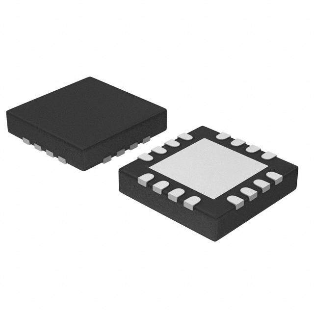
| 描述 | IC DETEC RF 100KHZ-1GHZ TSOT23-6 |
| 产品分类 | |
| 品牌 | Linear Technology |
| 数据手册 | http://www.linear.com/docs/2368 |
| 产品图片 |
|
| 产品型号 | LTC5507ES6#TRMPBF |
| RF类型 | 通用 |
| rohs | 无铅 / 符合限制有害物质指令(RoHS)规范要求 |
| 产品系列 | - |
| 产品目录页面 | |
| 其它名称 | LTC5507ES6#PBF |
| 包装 | 剪切带 (CT) |
| 封装/外壳 | SOT-23-6 细型,TSOT-23-6 |
| 标准包装 | 1 |
| 电压-电源 | 2.7 V ~ 6 V |
| 电流-电源 | 550µA |
| 精度 | - |
| 输入范围 | -34dBm ~ 14dBm |
| 频率 | 100kHz ~ 1GHz |


- 商务部:美国ITC正式对集成电路等产品启动337调查
- 曝三星4nm工艺存在良率问题 高通将骁龙8 Gen1或转产台积电
- 太阳诱电将投资9.5亿元在常州建新厂生产MLCC 预计2023年完工
- 英特尔发布欧洲新工厂建设计划 深化IDM 2.0 战略
- 台积电先进制程称霸业界 有大客户加持明年业绩稳了
- 达到5530亿美元!SIA预计今年全球半导体销售额将创下新高
- 英特尔拟将自动驾驶子公司Mobileye上市 估值或超500亿美元
- 三星加码芯片和SET,合并消费电子和移动部门,撤换高东真等 CEO
- 三星电子宣布重大人事变动 还合并消费电子和移动部门
- 海关总署:前11个月进口集成电路产品价值2.52万亿元 增长14.8%


PDF Datasheet 数据手册内容提取
LTC5507 100kHz to 1GHz RF Power Detector FEATURES DESCRIPTIOU n Temperature Compensated Internal Schottky The LTC®5507 is an RF power detector for applications Diode RF Detector operating from 100kHz to 1000MHz. The input frequency n Wide Input Power Range: –34dBm to 14dBm range is determined by an external capacitor. A tempera- n Ultra Wide Input Frequency Range: 100kHz to ture-compensated Schottky diode peak detector and buffer 1000MHz amplifier are combined in a small 6-pin ThinSOT package. n Buffered Output The RF input voltage is peak detected using an on-chip n Wide V Range of 2.7V to 6V CC Schottky diode and external capacitor. The detected volt- n Low Operating Current: 550m A age is buffered and supplied to the V pin. A power n Low Shutdown Current: <2m A OUT saving shutdown mode reduces supply current to less n Low Profile (1mm) ThinSOTTM Package than 2m A. APPLICATIOU S , LTC and LT are registered trademarks of Linear Technology Corporation. ThinSOT is a trademark of Linear Technology Corporation n Wireless Transceivers n Wireless and Cable Infrastructure n RF Power Alarm n Envelope Detector TYPICAL APPLICATIOU Typical Detector Characteristics at 100kHz, 100MHz and 1000MHz 10000 TA = 25°C VCC = 2.7V TO 6V 2.7V TVOB 6AVT C2 45 VCCLTC5507VOUT 32 VDVOOEUTLTETCATGEED AGE (mV) PCAP GND T C1 OL INPURTF 6 RFIN SHDN 1 DISABLE ENABLE PUT V1000 100kHz, 100MHz T 5507 TA01 U O 1000MHz UT O Figure 1. 100kHz to 1000MHz RF Power Detector V 100 –34 –26 –18 –10 –2 6 14 RF INPUT POWER (dBm) 5507 TA01b 5507f 1
LTC5507 ABSOLUTE WAXIWUW RATIUGS PACKAGE/ORDER IUFORWATIOU (Note 1) ORDER PART V , V to GND.................................... –0.3V to 6.5V CC OUT NUMBER RF Voltage to GND......................... (V – 1.8V) to 7V IN CC TOP VIEW SHDN Voltage to GND ................ –0.3V to (V + 0.3V) LTC5507ES6 CC PCAP Voltage to GND........................(V – 1.8V) to 7V SHDN 1 6 RFIN CC GND 2 5 PCAP I ...................................................................... 5mA VOUT VOUT 3 4 VCC Operating Temperature Range (Note 2)..–40(cid:176) C to 85(cid:176) C S6 PART Maximum Junction Temperature......................... 125(cid:176) C S6 PACKAGE MARKING 6-LEAD PLASTIC SOT-23 Storage Temperature Range................ –65(cid:176) C to 150(cid:176) C Lead Temperature (Soldering, 10 sec)................. 300(cid:176) C TJMAX = 125(cid:176)C, q JA = 250(cid:176)C/W LTZX Consult LTC Marketing for parts specified with wider operating temperature ranges. ELECTRICAL CHARACTERISTICS The l denotes the specifications which apply over the full operating temperature range, otherwise specifications are at T = 25(cid:176) C. V = 3.6V, RF Input Signal is Off, unless otherwise noted. A CC PARAMETER CONDITIONS MIN TYP MAX UNITS V Operating Voltage l 2.7 6 V CC I Shutdown Current SHDN = 0V l 2 m A VCC I Operating Current SHDN = V , I = 0mA l 0.55 0.85 mA VCC CC VOUT V V (No RF Input) R = 2k, SHDN = V , Enabled 130 250 370 mV OUT OL LOAD CC SHDN = 0V, Disabled 1 mV V Output Current V = 1.75V, V = 2.7V to 6V, D V = 10mV l 1 2 mA OUT OUT CC OUT V Enable Time SHDN = V , C = 33pF, R = 2k l 7 20 m s OUT CC LOAD LOAD V Load Capacitance (Note 4) l 33 pF OUT V Noise V = 3V, Noise BW = 1.5MHz, 50W RF Input Termination 2 mV OUT CC P-P SHDN Voltage, Chip Disabled V = 2.7V to 6V l 0.35 V CC SHDN Voltage, Chip Enabled V = 2.7V to 6V l 1.4 V CC SHDN Input Current SHDN = 3.6V l 24 40 m A RF Input Frequency Range 0.1– 1000 MHz IN Max RF Input Power (Note 3) 14 dBm IN RF AC Input Resistance F = 10MHz, RF Input = –10dBm 130 W IN F = 1000MHz, RF Input = –10dBm 95 W RF Input Shunt Capacitance 1.7 pF IN Note 1: Absolute Maximum Ratings are those values beyond which the life Note 3: RF performance is tested at: 80MHz, –4dBm of a device may be impaired. Note 4: Guaranteed by design. Note 2: Specifications over the –40(cid:176) C to 85(cid:176) C operating temperature range are assured by design, characterization and correlation with statistical process controls. 5507f 2
LTC5507 TYPICAL PERFORW AU CE CHARACTERISTICS LTC5507 Typical Detector LTC5507 Typical Detector Characteristics, 100kHz, Characteristics, 100MHz VCC = 2.7V TO 6V VCC = 2.7V TO 6V 10000 10000 C1 = 0.47µF C1 = 1000pF C2 = 0.47µF C2 = 1000pF V) V) m m E ( E ( G G A A T T L L O O V1000 V1000 T T U U P P T T OUUT TA = –40°C TA = 85°C OUUT TA = –40°C O O V TA = 25°C V TA = 85°C TA = 25°C 100 100 –34 –28 –22 –16 –10 –4 2 8 14 –34 –28 –22 –16 –10 –4 2 8 14 RF INPUT POWER (dBm) RF INPUT POWER (dBm) 5507 G01 5507 G02 LTC5507 Typical Detector Characteristics, 1000MHz Positive VOUT Slew Rate vs C2 V = 2.7V TO 6V Capacitance CC 10000 10.0 C1 = 33pF C2 = 33pF s) GE (mV) mATE (V/ 1.0 A R LT W O E OUTPUT VUT1000 TA = –40°C TA = 85°C TIVE V SLOUT0.10 VO OSI P TA = 25°C 100 0.01 –34 –28 –22 –16 –10 –4 2 8 14 33 330 3300 33000 330000 RF INPUT POWER (dBm) C2 CAPACITANCE (pF) 5507 G03 5507 G04 Negative V Slew Rate vs C2 OUT Capacitance V BW vs C2 Capacitance OUT 10.000 10000 s) mE (V/1.000 1000 T W RA0.100 kHz) LE W ( 100 E V SOUT0.010 V BOUT V TI 10 GA0.001 E N 0 1 33 330 3300 33000 330000 33 330 3300 33000 330000 C2 CAPACITANCE (pF) C2 CAPACITANCE (pF) 5507 G05 5507 G06 5507f 3
LTC5507 PIU FUU CTIOU S SHDN (Pin 1): Shutdown Input. A logic low or no-connect V (Pin 4): Power Supply Voltage, 2.7V to 6V. V should CC CC on the SHDN pin places the part in shutdown mode. A logic be bypassed with 0.1m F and 100pF ceramic capacitors. high enables the part. SHDN has an internal 150k pull PCAP (Pin 5): Peak Detector Hold Capacitor. Capacitor down resistor to ensure that the part is in shutdown when value is dependent on RF frequency. Capacitor must be the enable driver is in a tri-state condition. connected between PCAP and V . CC GND (Pin 2): System Ground. RF (Pin 6): RF Input Voltage. Referenced to V . A IN CC V (Pin 3): Buffered and Level Shifted Detector Output coupling capacitor must be used to connect to the RF OUT Voltage. signal source. This pin has an internal 250W termination and an internal Schottky diode detector. BLOCK DIAGRAW VCC 4 GAIN + COMPRESSION C1 250Ω –BUFFER 3 VOUT RFSOURCE 6 RFIN SHDN 30k C2 30k 100Ω VCC 5 + PCAP RF DET – 60µA 60µA 150k BIAS GND 2 1 C1 = C2 5507 BD SHDN C2 (µF) ‡ 1 , f = LOWEST RF INPUT FREQUENCY (MHz) 30f Figure 2. 5507f 4
LTC5507 APPLICATIOUS IUFORWATIOU Operation Applications The LTC5507 integrates several functions to provide RF The LTC5507 can be used as a self-standing signal strength power detection over frequencies up to 1000MHz. These measuring receiver for a wide range of input signals from functions include an internally compensated buffer ampli- –34dBm to 14dBm for frequencies up to 1000MHz. fier, an RF Schottky diode peak detector and level shift The LTC5507 can be used as a demodulator for AM and amplifier to convert the RF signal to DC, a delay circuit to ASK modulated signals with data rates up to 1.5MHz. avoid voltage transients at V when coming out of shut- OUT Depending on specific application needs, the RSSI output down, and a gain compression circuit to extend the can be split into two branches, providing AC-coupled data detector dynamic range. (or audio) output and DC-coupled, RSSI output for signal strength measurements and AGC. Buffer Amplifier The buffer amplifier has a gain of two and is capable of C1, C2 Capacitor Selection (Refer to Figure 3) driving a 2mA load. The buffer amplifier typically has an C1 couples the RF input signal to the detector input RF IN output voltage range of 0.25V to V – 0.1V. CC which is referenced to V . C2 is the peak detector CC capacitor connected between PCAP and V . The value of RF Detector CC C2 will affect the slew rate and bandwidth. Typically C1 can The internal RF Schottky diode peak detector and level equal C2. Ceramic capacitors are recommended for C1 shift amplifier converts the RF input signal to a low and C2. The values for C1 and C2 are dependent on the frequency signal. The frequency range of the RF pin is operating RF frequency. The capacitive reactance should typically up to 1000MHz. The detector demonstrates ex- be less than 5W to minimize ripple on C2. cellent operation over a wide range of input power. The C2(m F) ‡ 1/(30 • f) where f is the lowest RF input Schottky detector is biased at about 70m A. The hold frequency (MHz) capacitor is external. C1 = C2 Gain Compression In general, select C1 and C2 large enough to pass the The gain compression circuit changes the feedback ratio lowest expected RF signal frequency, as described by the as the RF peak-detected input voltage increases above above formulas. But optimize C1 and C2, subject to this 60mV. Below 60mV, the DC voltage gain from the peak constraint, to improve output slew rate and bandwidth, detector to the buffer output is 4. Above 140mV, the DC and to enable good AC performance for the highest voltage gain is reduced to 0.75. The compression expands expected RF signal frequency. the low power detector range due to higher gain. Modes of Operation MODE SHDN OPERATION Shutdown Low Disabled Enable High Power Detect 5507f 5
LTC5507 APPLICATIOUS IUFORWATIOU R3* J1 E4 22k R4* SHDN VCC RFIN C1 LTC5507 1 6 JP1 SHDN RFIN 2 5 SHDN R2* GND PCAP VCC E2 68Ω 3 4 C2 E1 VOUT VOUT VCC VCC E3 C5* C4* C3* GND 0.1µF 100pF 5507 F03 *OPTIONAL COMPONENTS R2 AND C5 FORM AN OPTIONAL OUTPUT LOWPASS FILTER. R3 IS USED FOR DEMO PURPOSES ONLY, AND IS NOT USED IN ACTUAL PRODUCT IMPLEMENTATION. R4 CAN BE USED FOR INPUT POWER LIMITING OR BROADBAND IMPEDANCE MATCHING. C3 AND C4 ARE OPTIONAL POWER SUPPLY FILTERS. Figure 3. Evaluation Demo Board Schematic 5507f 6
LTC5507 PACKAGE DESCRIPTIOU S6 Package 6-Lead Plastic TSOT-23 (Reference LTC DWG # 05-08-1636) 2.90 BSC 0.62 0.95 (NOTE 4) MAX REF 1.22 REF 1.50 – 1.75 3.85 MAX 2.62 REF 1.4 MIN 2.80 BSC (NOTE 4) PIN ONE ID RECOMMENDED SOLDER PAD LAYOUT 0.30 – 0.45 0.95 BSC PER IPC CALCULATOR 6 PLCS (NOTE 3) 0.80 – 0.90 0.20 BSC 0.01 – 0.10 1.00 MAX DATUM ‘A’ 0.30 – 0.50 REF 1.90 BSC 0.09 – 0.20 (NOTE 3) S6 TSOT-23 0302 NOTE: 1. DIMENSIONS ARE IN MILLIMETERS 2. DRAWING NOT TO SCALE 3. DIMENSIONS ARE INCLUSIVE OF PLATING 4. DIMENSIONS ARE EXCLUSIVE OF MOLD FLASH AND METAL BURR 5. MOLD FLASH SHALL NOT EXCEED 0.254mm 6. JEDEC PACKAGE REFERENCE IS MO-193 5507f Information furnished by Linear Technology Corporation is believed to be accurate and reliable. 7 However, no responsibility is assumed for its use. Linear Technology Corporation makes no represen- tation that the interconnection of its circuits as described herein will not infringe on existing patent rights.
LTC5507 RELATED PARTS PART NUMBER DESCRIPTION COMMENTS RF Power Controllers LTC1757A RF Power Controller Multiband GSM/DCS/GPRS Mobile Phones LTC1758 RF Power Controller Multiband GSM/DCS/GPRS Mobile Phones LTC1957 RF Power Controller Multiband GSM/DCS/GPRS Mobile Phones LTC4400 ThinSOT RF PA Controller Multiband GSM/DCS/GPRS Phones, 45dB Dynamic Range, 450kHz Loop BW LTC4401 ThinSOT RF PA Controller Multiband GSM/DCS/GPRS Phones, 45dB Dynamic Range, 250kHz Loop BW LTC4403 Multiband RF Power Controllers for EDGE/TDMA Supports EDGE/TDMA Applications LT5504 800MHz to 2.7GHz RF Measuring Receivers 80dB Dynamic Range, Temperature Compensated, 2.7V to 5.5V Supply LTC5505 300MHz to 3.5GHz RF Power Detector >40dB Dynamic Range, Temperature Compensated, 2.7V to 6V Supply LTC5508 300MHz to 7GHz RF Power Detector >40dB Dynamic Range, SC-70 Package Other Related Parts LT5500 1.8GHz to 2.7GHz, Receiver Front End Dual LNA gain Setting +13.5dB/–14dB at 2.5GHz, Double-Balanced Mixer, 1.8V to 5.25V Supply LT5502 400MHz Quadrature Demodulator with RSSI 1.8V to 5.25V Supply, 70MHz to 400MHz IF, 84dB Limiting Gain, 90dB RSSI Range LT5503 1.2GHz to 2.7GHz Direct IQ Modulator and 1.8V to 5.25V Supply, Four-Step RF Power Control, 120MHz Modulation Bandwidth Up Converting Mixer LT5506 500MHz Quadrature IF Demodulator with VGA 1.8V to 5.25V Supply, 40MHz to 500MHz IF, –4dB to 57dB Linear Power Gain LT5511 High Signal Level Upconverting Mixer 10MHz to 3000MHz RF Output Range, Integrated LO Buffer, 17dBm IIP3 LT5512 High Signal Level Down Converting Mixer DC-3GHz, 20dBm IIP3, Integrated LO Buffer 5507f 8 Linear Technology Corporation LT/TP 0103 2K • PRINTED IN USA 1630 McCarthy Blvd., Milpitas, CA 95035-7417 (408) 432-1900 l FAX: (408) 434-0507 l www.linear.com ª LINEAR TECHNOLOGY CORPORATION 2001
Mouser Electronics Authorized Distributor Click to View Pricing, Inventory, Delivery & Lifecycle Information: A nalog Devices Inc.: LTC5507ES6 LTC5507ES6#PBF LTC5507ES6#TR LTC5507ES6#TRM LTC5507ES6#TRMPBF LTC5507ES6#TRPBF