ICGOO在线商城 > 射频/IF 和 RFID > RF 检测器 > AD8319ACPZ-R7
 Datasheet下载
- 型号: AD8319ACPZ-R7
- 制造商: Analog
- 库位|库存: xxxx|xxxx
- 要求:
| 数量阶梯 | 香港交货 | 国内含税 |
| +xxxx | $xxxx | ¥xxxx |
查看当月历史价格
查看今年历史价格
AD8319ACPZ-R7产品简介:
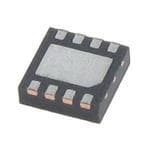
ICGOO电子元器件商城为您提供AD8319ACPZ-R7由Analog设计生产,在icgoo商城现货销售,并且可以通过原厂、代理商等渠道进行代购。 AD8319ACPZ-R7价格参考。AnalogAD8319ACPZ-R7封装/规格:RF 检测器, RF Detector IC RADAR, 802.11/WiFi, 8.2.16/WiMax, Wireless LAN 1MHz ~ 10GHz -60dBm ~ -2dBm ±1dB 8-VFDFN Exposed Pad, CSP。您可以下载AD8319ACPZ-R7参考资料、Datasheet数据手册功能说明书,资料中有AD8319ACPZ-R7 详细功能的应用电路图电压和使用方法及教程。
AD8319ACPZ-R7是Analog Devices Inc.推出的一款高性能RF检波器,主要应用于射频信号的功率检测与控制。该器件可在400 MHz至6 GHz的宽频率范围内工作,适用于无线通信系统中的发射功率监测与调节,如蜂窝基站、微波点对点通信和无线基础设施设备。其对数放大器架构可提供精确的动态范围(约56 dB),输出电压与输入RF信号的对数成正比,便于实现自动增益控制(AGC)或功率稳定功能。

此外,AD8319ACPZ-R7响应速度快、温度稳定性好,适合用于需要实时功率反馈的系统,例如雷达模块、测试测量仪器及射频识别(RFID)系统。其采用紧凑的8引脚LFCSP封装,便于在高密度PCB布局中使用,同时具备低功耗特性,适用于对空间和能耗敏感的应用场景。整体而言,该芯片广泛用于需精准、快速检测高频信号强度的工业与通信领域。
| 参数 | 数值 |
| 产品目录 | |
| 描述 | IC LOG DETCTR/CTRL 10GHZ 8LFCSP对数放大器 1MHz TO 10GHz 40dB |
| DevelopmentKit | AD8319-EVALZ |
| 产品分类 | |
| 品牌 | Analog Devices Inc |
| 产品手册 | |
| 产品图片 |
|
| rohs | 符合RoHS无铅 / 符合限制有害物质指令(RoHS)规范要求 |
| 产品系列 | 放大器 IC,对数放大器,Analog Devices AD8319ACPZ-R7- |
| 数据手册 | |
| 产品型号 | AD8319ACPZ-R7 |
| RF类型 | RADAR, 802.11/WiFi, 8.2.16/WiMax, 无线 LAN |
| 产品 | Logarithmic Amplifiers |
| 产品培训模块 | http://www.digikey.cn/PTM/IndividualPTM.page?site=cn&lang=zhs&ptm=25139 |
| 产品种类 | 对数放大器 |
| 其它名称 | AD8319ACPZ-R7CT |
| 功率耗散 | 0.73 W |
| 包装 | 剪切带 (CT) |
| 商标 | Analog Devices |
| 安装风格 | SMD/SMT |
| 封装 | Reel |
| 封装/外壳 | 8-VFDFN 裸露焊盘,CSP |
| 封装/箱体 | LFCSP-8 |
| 工作温度范围 | - 40 C to + 85 C |
| 工作电源电压 | 3 V to 5.5 V |
| 工厂包装数量 | 3000 |
| 带宽 | 1 MHz to 10 GHz |
| 放大器类型 | Logarithmic |
| 最小工作温度 | - 40 C |
| 标准包装 | 1 |
| 电压-电源 | 3 V ~ 5.5 V |
| 电流-电源 | 22mA |
| 电源电流 | 22 mA |
| 类型 | Log Amp Detector |
| 精度 | ±1dB |
| 系列 | AD8319 |
| 视频文件 | http://www.digikey.cn/classic/video.aspx?PlayerID=1364138032001&width=640&height=505&videoID=2245193150001 |
| 输入电压范围—最大 | 5.5 V |
| 输入范围 | -60dBm ~ -2dBm |
| 通道数量 | 1 Channel |
| 频率 | 1MHz ~ 10GHz |


- 商务部:美国ITC正式对集成电路等产品启动337调查
- 曝三星4nm工艺存在良率问题 高通将骁龙8 Gen1或转产台积电
- 太阳诱电将投资9.5亿元在常州建新厂生产MLCC 预计2023年完工
- 英特尔发布欧洲新工厂建设计划 深化IDM 2.0 战略
- 台积电先进制程称霸业界 有大客户加持明年业绩稳了
- 达到5530亿美元!SIA预计今年全球半导体销售额将创下新高
- 英特尔拟将自动驾驶子公司Mobileye上市 估值或超500亿美元
- 三星加码芯片和SET,合并消费电子和移动部门,撤换高东真等 CEO
- 三星电子宣布重大人事变动 还合并消费电子和移动部门
- 海关总署:前11个月进口集成电路产品价值2.52万亿元 增长14.8%


PDF Datasheet 数据手册内容提取
1 MHz to 10 GHz, 45 dB Log Detector/Controller Data Sheet AD8319 FEATURES FUNCTIONAL BLOCK DIAGRAM Wide bandwidth: 1 MHz to 10 GHz VPOS TADJ High accuracy: ±1.0 dB over temperature 45 dB dynamic range up to 8 GHz GBIAAISN SLOPE I V VSET Stability over temperature: ±0.5 dB Low noise measurement/controller output VOUT I V VOUT Pulse response time (fall/rise): 6 ns/10 ns DET DET DET DET Small footprint: 2 mm × 3 mm LFCSP CLPF INHI Supply operation: 3.0 V to 5.5 V @ 22 mA INLO Fabricated using high speed SiGe process COMM 05705-001 APPLICATIONS Figure 1. RF transmitter PA setpoint controls and level monitoring Power monitoring in radiolink transmitters RSSI measurement in base stations, WLANs, WiMAX, and radars GENERAL DESCRIPTION The AD8319 is a demodulating logarithmic amplifier, capable The feedback loop through an RF amplifier is closed via VOUT, of accurately converting an RF input signal to a corresponding the output of which regulates the output of the amplifier to a decibel-scaled output. It employs the progressive compression magnitude corresponding to V . The AD8319 provides 0 V to SET technique over a cascaded amplifier chain, each stage of which (V − 0.1 V) output capability at the VOUT pin, suitable for POS is equipped with a detector cell. The device can be used in either controller applications. As a measurement device, VOUT is measurement or controller modes. The AD8319 maintains externally connected to VSET to produce an output voltage, accurate log conformance for signals of 1 MHz to 8 GHz and V , that is a decreasing linear-in-dB function of the RF input OUT provides useful operation to 10 GHz. The input dynamic range signal amplitude. is typically 45 dB (re: 50 Ω) with error less than ±3 dB. The The logarithmic slope is −22 mV/dB, determined by the VSET AD8319 has 6 ns/10 ns (fall time/rise time) response time that interface. The intercept is 15 dBm (re: 50 Ω, CW input) using enables RF burst detection to a pulse rate of beyond 50 MHz. the INHI input. These parameters are very stable against supply The device provides unprecedented logarithmic intercept stability and temperature variations. vs. ambient temperature conditions. A supply of 3.0 V to 5.5 V The AD8319 is fabricated on a SiGe bipolar IC process and is is required to power the device. Current consumption is typically available in a 2 mm × 3 mm, 8-lead LFCSP for an operating 22 mA, and it decreases to 200 µA when the device is disabled. temperature range of −40°C to +85°C. The AD8319 can be configured to provide a control voltage to a power amplifier or a measurement output from the VOUT pin. Because the output can be used for controller applications, special attention was paid to minimize wideband noise. In this mode, the setpoint control voltage is applied to the VSET pin. Rev. D Document Feedback Information furnished by Analog Devices is believed to be accurate and reliable. However, no responsibility is assumed by Analog Devices for its use, nor for any infringements of patents or other One Technology Way, P.O. Box 9106, Norwood, MA 02062-9106, U.S.A. rights of third parties that may result from its use. Specifications subject to change without notice. No license is granted by implication or otherwise under any patent or patent rights of Analog Devices. Tel: 781.329.4700 ©2005–2017 Analog Devices, Inc. All rights reserved. Trademarks and registered trademarks are the property of their respective owners. Technical Support www.analog.com
AD8319 Data Sheet TABLE OF CONTENTS Features .............................................................................................. 1 Input Signal Coupling ................................................................ 11 Applications ....................................................................................... 1 Output Interface ......................................................................... 11 Functional Block Diagram .............................................................. 1 Setpoint Interface ....................................................................... 11 General Description ......................................................................... 1 Temperature Compensation of Output Voltage ..................... 12 Revision History ............................................................................... 2 Measurement Mode ................................................................... 12 Specifications ..................................................................................... 3 Setting the Output Slope in Measurement Mode .................. 13 Absolute Maximum Ratings ............................................................ 5 Controller Mode ......................................................................... 13 ESD Caution .................................................................................. 5 Output Filtering .......................................................................... 15 Pin Configuration and Function Descriptions ............................. 6 Operation Beyond 8 GHz.......................................................... 16 Typical Performance Characteristics ............................................. 7 Evaluation Board ............................................................................ 17 Theory of Operation ...................................................................... 10 Outline Dimensions ....................................................................... 19 Using the AD8319 .......................................................................... 11 Ordering Guide .......................................................................... 19 Basic Connections ...................................................................... 11 REVISION HISTORY 9/2017—Rev. C to Rev. D Changed CP-8-1 to CP-8-23 ........................................ Throughout Changes to Figure 2 .......................................................................... 6 Updated Outline Dimensions ....................................................... 19 Changes to Ordering Guide .......................................................... 19 3/2013—Rev. B to Rev. C Updated Outline Dimensions ....................................................... 18 4/2008—Rev. A to Rev. B Changes to Features Section and General Description Section . 1 Changes to Theory of Operation Section .................................... 10 Changes to Figure 22 and Setpoint Interface Section ................ 11 3/2007—Rev. 0 to Rev. A Changes to Figure 9 .......................................................................... 8 Changes to Figure 22 and Setpoint Interface Section ................ 11 Changes to Measurement Mode Section ..................................... 12 Changes to Layout .......................................................................... 16 Changes to Layout .......................................................................... 17 Updated Outline Dimensions ....................................................... 18 10/2005—Revision 0: Initial Version Rev. D | Page 2 of 19
Data Sheet AD8319 SPECIFICATIONS V = 3 V, C = 1000 pF, T = 25°C, 52.3 Ω termination resistor at INHI, unless otherwise noted. POS LPF A Table 1. Parameter Conditions Min Typ Max Unit SIGNAL INPUT INTERFACE INHI (Pin 1) Specified Frequency Range 0.001 10 GHz DC Common-Mode Voltage V − 0.6 V POS MEASUREMENT MODE VOUT (Pin 5) shorted to VSET (Pin 4), sinusoidal input signal f = 900 MHz R = 18 kΩ TADJ Input Impedance 1500||0.33 Ω||pF ±1 dB Dynamic Range TA = 25°C 40 dB −40°C < T < +85°C 40 dB A Maximum Input Level ±1 dB error −3 dBm Minimum Input Level ±1 dB error −43 dBm Slope1 −25 −22 −19.5 mV/dB Intercept1 12 15 21 dBm Output Voltage: High Power In P = −10 dBm 0.57 V IN Output Voltage: Low Power In P = −40 dBm 1.25 V IN f = 1.9 GHz R = 8 kΩ TADJ Input Impedance 950||0.38 Ω||pF ±1 dB Dynamic Range TA = 25°C 40 dB −40°C < T < +85°C 40 dB A Maximum Input Level ±1 dB error −4 dBm Minimum Input Level ±1 dB error −44 dBm Slope1 −25 −22 −19.5 mV/dB Intercept1 10 13 20 dBm Output Voltage: High Power In P = −10 dBm 0.53 V IN Output Voltage: Low Power In P = −35 dBm 1.19 V IN f = 2.2 GHz R = 8 kΩ TADJ Input Impedance 810||0.39 Ω||pF ±1 dB Dynamic Range TA = 25°C 40 dB −40°C < T < +85°C 40 dB A Maximum Input Level ±1 dB error −5 dBm Minimum Input Level ±1 dB error −45 dBm Slope1 −22 mV/dB Intercept1 13 dBm Output Voltage: High Power In P = −10 dBm 0.5 V IN Output Voltage: Low Power In P = −35 dBm 1.18 V IN f = 3.6 GHz R = 8 kΩ TADJ Input Impedance 300||0.33 Ω||pF ±1 dB Dynamic Range TA = 25°C 40 dB −40°C < T < +85°C 36 dB A Maximum Input Level ±1 dB error −6 dBm Minimum Input Level ±1 dB error −46 dBm Slope1 −22 mV/dB Intercept1 10 dBm Output Voltage: High Power In P = −10 dBm 0.46 V IN Output Voltage: Low Power In P = −40 dBm 1.14 V IN Rev. D | Page 3 of 19
AD8319 Data Sheet Parameter Conditions Min Typ Max Unit f = 5.8 GHz R = 500 Ω TADJ Input Impedance 110||0.05 Ω||pF ±1 dB Dynamic Range TA = 25°C 40 dB −40°C < T < +85°C 40 dB A Maximum Input Level ±1 dB error −3 dBm Minimum Input Level ±1 dB error −43 dBm Slope1 −22 mV/dB Intercept1 15 dBm Output Voltage: High Power In P = −10 dBm 0.57 V IN Output Voltage: Low Power In P = −40 dBm 1.25 V IN f = 8.0 GHz R = open TADJ Input Impedance 28||0.79 Ω||pF ±1 dB Dynamic Range TA = 25°C 40 dB −40°C < T < +85°C 31 dB A Maximum Input Level ±1 dB error −1 dBm Minimum Input Level ±1 dB error −41 dBm Slope2 −22 mV/dB Intercept2 20 dBm Output Voltage: High Power In P = −10 dBm 0.67 V IN Output Voltage: Low Power In P = −40 dBm 1.34 V IN OUTPUT INTERFACE VOUT (Pin 5) Voltage Swing V = 0 V; RFIN = open V − 0.1 V SET POS V = 1.5 V; RFIN = open 10 mV SET Output Current Drive V = 0 V; RFIN = open 10 mA SET Small Signal Bandwidth RFIN = −10 dBm; from CLPF to VOUT 140 MHz Output Noise RFIN = 2.2 GHz, −10 dBm, f = 100 kHz, 90 nV/√Hz NOISE C = open LPF Fall Time Input level = no signal to −10 dBm, 90% to 10%; 18 ns C = 8 pF LPF Input level = no signal to −10 dBm, 90% to 10%; 6 ns C = open; R = 150 Ω LPF OUT Rise Time Input level = −10 dBm to no signal, 10% to 90%; 20 ns C = 8 pF LPF Input level = −10 dBm to no signal, 10% to 90%; 10 ns C = open; R = 150 Ω LPF OUT Video Bandwidth (or Envelope Bandwidth) 50 MHz VSET INTERFACE VSET (Pin 4) Nominal Input Range RFIN = 0 dBm; measurement mode 0.35 V RFIN = −40 dBm; measurement mode 1.23 V Logarithmic Scale Factor −45 dB/V Input Resistance RFIN = −20 dBm; controller mode; V = 1 V 40 kΩ SET TADJ INTERFACE TADJ (Pin 6) Input Resistance TADJ = 0.9 V, sourcing 50 µA 40 kΩ Disable Threshold Voltage TADJ = open V − 0.4 V POS POWER INTERFACE VPOS (Pin 7) Supply Voltage 3.0 5.5 V Quiescent Current 18 22 30 mA vs. Temperature −40°C ≤ T ≤ +85°C 60 µA/°C A Disable Current TADJ = VPOS 200 µA 1 Slope and intercept are determined by calculating the best fit line between the power levels of −40 dBm and −10 dBm at the specified input frequency. 2 Slope and intercept are determined by calculating the best fit line between the power levels of −34 dBm and −16 dBm at 8.0 GHz. Rev. D | Page 4 of 19
Data Sheet AD8319 ABSOLUTE MAXIMUM RATINGS Stresses at or above those listed under Absolute Maximum Table 2. Ratings may cause permanent damage to the product. This is a Parameter Rating stress rating only; functional operation of the product at these Supply Voltage: V 5.7 V POS or any other conditions above those indicated in the operational V Voltage 0 to V SET POS section of this specification is not implied. Operation beyond Input Power (Single-Ended, re: 50 Ω) 12 dBm the maximum operating conditions for extended periods may Internal Power Dissipation 0.73 W affect product reliability. θ 55°C/W JA Maximum Junction Temperature 125°C ESD CAUTION Operating Temperature Range −40°C to +85°C Storage Temperature Range −65°C to +150°C Lead Temperature (Soldering, 60 sec) 260°C Rev. D | Page 5 of 19
AD8319 Data Sheet PIN CONFIGURATION AND FUNCTION DESCRIPTIONS INHI 1 8 INLO COMM 2 7 VPOS AD8319 CLPF 3 TOP VIEW 6 TADJ (Not to Scale) VSET 4 5 VOUT NOTES 1.TCGHOREMO PUMAN; DDS OIPSLL IDANENTREE .RTNOA AL LLYO WCO IMNNPEECDTAENDC ETO 05705-002 Figure 2. Pin Configuration Table 3. Pin Function Descriptions Pin No. Mnemonic Description 1 INHI RF Input. Nominal input range of −50 dBm to 0 dBm, re: 50 Ω; ac-coupled RF input. 2 COMM Device Common. Connect this pin to a low impedance ground plane. 3 CLPF Loop Filter Capacitor. In measurement mode, this capacitor sets the pulse response time and video bandwidth. In controller mode, the capacitance on this node sets the response time of the error amplifier/integrator. 4 VSET Setpoint Control Input for Controller Mode or Feedback Input for Measurement Mode. 5 VOUT Measurement and Controller Output. In measurement mode, VOUT provides a decreasing linear-in-dB representation of the RF input signal amplitude. In controller mode, VOUT is used to control the gain of a VGA or VVA with a positive gain sense (increasing voltage increases gain). 6 TADJ Temperature Compensation Adjustment. Frequency dependent temperature compensation is set by connecting a ground referenced resistor to this pin. 7 VPOS Positive Supply Voltage, 3.0 V to 5.5 V. 8 INLO RF Common for INHI. AC-coupled RF common. EPAD The pad is internally connected to COMM; solder to a low impedance ground plane. Rev. D | Page 6 of 19
Data Sheet AD8319 TYPICAL PERFORMANCE CHARACTERISTICS V = 3 V; T = 25°C, −40°C, +85°C; C = 1000 pF; unless otherwise noted. Black: 25°C; Blue: −40°C; Red: +85°C. Error is calculated by POS LPF using the best fit line between P = −40 dBm and P = −10 dBm at the specified input frequency, unless otherwise noted. IN IN 2.00 2.0 2.00 2.0 1.75 1.5 1.75 1.5 1.50 1.0 1.50 1.0 (V)UT 11..0205 00.5 OR (dB) (V)UT 11..0205 00.5 OR (dB) VO RR VO RR 0.75 –0.5 E 0.75 –0.5 E 0.50 –1.0 0.50 –1.0 0.25 –1.5 0.25 –1.5 0–60 –50 –40 –3P0IN (dBm–2)0 –10 0 10–2.0 05705-003 0–60 –50 –40 –3P0IN (dBm–2)0 –10 0 10–2.0 05705-006 Figure 3. VOUT and Log Conformance Error vs. Figure 6. VOUT and Log Conformance Error vs. Input Amplitude at 900 MHz, RTADJ = 18 kΩ Input Amplitude at 3.6 GHz, RTADJ = 8 kΩ 2.00 2.0 2.00 2.0 1.75 1.5 1.75 1.5 1.50 1.0 1.50 1.0 (V)UT 11..0205 00.5 OR (dB) (V)UT 11..0205 00.5 OR (dB) VO RR VO RR 0.75 –0.5 E 0.75 –0.5 E 0.50 –1.0 0.50 –1.0 0.25 –1.5 0.25 –1.5 0–60 –50 –40 –3P0IN(dBm–2)0 –10 0 10–2.0 05705-004 0–60 –50 –40 –3P0IN (dBm–2)0 –10 0 10–2.0 05705-007 Figure 4. VOUT and Log Conformance Error vs. Figure 7. VOUT and Log Conformance Error vs. Input Amplitude at 1.9 GHz, RTADJ = 8 kΩ Input Amplitude at 5.8 GHz, RTADJ = 500 Ω 2.00 2.0 2.00 2.0 1.75 1.5 1.75 1.5 1.50 1.0 1.50 1.0 (V)UT 11..0205 00.5 OR (dB) (V)UT 11..0205 00.5 OR (dB) VO RR VO RR 0.75 –0.5 E 0.75 –0.5 E 0.50 –1.0 0.50 –1.0 0.25 –1.5 0.25 –1.5 0–60 –50 –40 –3P0IN (dBm–2)0 –10 0 10–2.0 05705-005 0–60 –50 –40 –3P0IN (dBm–2)0 –10 0 10–2.0 05705-008 Figure 5. VOUT and Log Conformance Error vs. Figure 8. VOUT and Log Conformance Error vs. Input Amplitude at 8.0 GHz, Input Amplitude at 2.2 GHz, RTADJ = 8 kΩ RTADJ = Open, Error Calculated from PIN = −34 dBm to PIN = −16 dBm Rev. D | Page 7 of 19
AD8319 Data Sheet 2.00 2.0 2.00 2.0 1.75 1.5 1.75 1.5 1.50 1.0 1.50 1.0 1.25 0.5 B) 1.25 0.5 B) (V)UT 1.00 0 OR(d (V)UT 1.00 0 OR (d VO RR VO RR 0.75 –0.5 E 0.75 –0.5 E 0.50 –1.0 0.50 –1.0 0.25 –1.5 0.25 –1.5 0–60 –50 –40 –3P0IN (dBm–2)0 –10 0 10–2.0 05705-009 0–60 –50 –40 –3P0IN (dBm–2)0 –10 0 10–2.0 05705-012 Figure 9. VOUT and Log Conformance Error vs. Input Amplitude at 900 MHz, Figure 12. VOUT and Log Conformance Error vs. Input Amplitude at 3.6 GHz, Multiple Devices, RTADJ = 18 kΩ Multiple Devices, RTADJ = 8 kΩ 2.00 2.0 2.00 2.0 1.75 1.5 1.75 1.5 1.50 1.0 1.50 1.0 1.25 0.5 B) 1.25 0.5 B) (V)UT 1.00 0 OR (d (V)UT 1.00 0 OR (d VO RR VO RR 0.75 –0.5 E 0.75 –0.5 E 0.50 –1.0 0.50 –1.0 0.25 –1.5 0.25 –1.5 0–60 –50 –40 –3P0IN (dBm–2)0 –10 0 10–2.0 05705-010 0–60 –50 –40 –3P0IN (dBm–2)0 –10 0 10–2.0 05705-013 Figure 10. VOUT and Log Conformance Error vs. Input Amplitude at 1.9 GHz, Figure 13. VOUT and Log Conformance Error vs. Input Amplitude at 5.8 GHz, Multiple Devices, RTADJ = 8 kΩ Multiple Devices, RTADJ = 500 Ω 2.00 2.0 2.00 2.0 1.75 1.5 1.75 1.5 1.50 1.0 1.50 1.0 V (V)OUT 11..0205 00.5 RROR (dB) V (V)OUT 11..0205 00.5 RROR (dB) 0.75 –0.5 E 0.75 –0.5 E 0.50 –1.0 0.50 –1.0 0.25 –1.5 0.25 –1.5 0–60 –50 –40 –3P0IN (dBm–2)0 –10 0 10–2.0 05705-011 0–60 –50 –40 –3P0IN (dBm–2)0 –10 0 10–2.0 05705-014 Figure 11. VOUT and Log Conformance Error vs. Input Amplitude at 2.2 GHz, Figure 14. VOUT and Log Conformance Error vs. Input Amplitude at 8.0 GHz, Multiple Devices, RTADJ = 8 kΩ Multiple Devices, RTADJ = Open, Error Calculated from PIN = −34 dBm to PIN = −16 dBm Rev. D | Page 8 of 19
Data Sheet AD8319 j1 j0.5 j2 10k j0.2 Hz) V/ n –60dBm TY ( 1k 0 0.2 0.5 1 2 ENSI D RF OFF L 100MHz RA –20dBm T –10dBm –j0.2 900MHz EC 100 –40dBm P S E 1900MHz OIS 0dBm 8000MHz –j0.5 –j23600M22H0z0MHz N 10 05705-018 SSTTAORPT F FRREEQQUUEENNCCYY = = 1 00G.0H5Gz1H0z000MHz–j1 5800MHz 05705-015 1k 10k FREQU1E0N0kCY (Hz) 1M 10M Figure 15. Input Impedance vs. Frequency; No Termination Resistor on INHI Figure 18. Noise Spectral Density of Output vs. Frequency; CLPF = Open (Impedance De-Embedded to Input Pins), Z0 = 50 Ω ∆ : 1.53V 10k @ : 1.53V Hz) V/ n TY ( 1k SI N E D L A R T C E 100 P 1 E S S OI N 05705-016 10 05705-019 Ch1 500mV M2.00µs A CH1 420V 1k 10k 100k 1M 10M T 29.60% FREQUENCY (Hz) Figure 16. Power On/Off Response Time; VP = 3.0 V; Figure 19. Noise Spectral Density of Output Buffer vs. Frequency (from CLPF Input AC-Coupling Capacitors = 10 pF; CLPF = Open to VOUT); CLPF = 0.1 μF 2.00 2.0 CH1 RISE 3.3V 9.949ns 1.75 1.5 3.0V CH1FALL 6.032ns 1.50 3.6V 1.0 1.25 0.5 B) (V)UT1.00 0 OR (d O R V R 0.75 –0.5 E 0.50 –1.0 0.25 –1.5 1Ch1 200mV MT 2 07.20.n40s% A CH1 1.04V 05705-017 0–60 –55 –50 –45 –40 –35 –3P0IN– (2d5Bm–2)0 –15 –10 –5 0 5 10–2.0 05705-020 Figure 17. VOUT Pulse Response Time; Pulsed RF Input 0.1 GHz, −10 dBm; Figure 20. VOUT Stability and Error vs. Supply Voltage at 1.9 GHz CLPF = Open; RLOAD = 150 Ω When VPOS Varies by 10% Rev. D | Page 9 of 19
AD8319 Data Sheet THEORY OF OPERATION The logarithmic function is approximated in a piecewise fashion The AD8319 is a five-stage demodulating logarithmic amplifier, by five cascaded gain stages. (For a detailed explanation of the specifically designed for use in RF measurement and power control logarithm approximation, refer to the AD8307 data sheet.) The applications at frequencies up to 10 GHz. A block diagram is cells have a nominal voltage gain of 9 dB each and a 3 dB shown in Figure 21. Sharing much of its design with the AD8318 bandwidth of 10.5 GHz. Using precision biasing, the gain is logarithmic detector/controller, the AD8319 maintains tight stabilized over temperature and supply variations. The overall intercept variability vs. temperature over a 40 dB range. Additional dc gain is high due to the cascaded nature of the gain stages. enhancements over the AD8318, such as reduced RF burst An offset compensation loop is included to correct for offsets response time of 6 ns to 10 ns, 22 mA supply current, and within the cascaded cells. At the output of each of the gain board space requirements of only 2 mm × 3 mm add to the low stages, a square-law detector cell is used to rectify the signal. cost and high performance benefits found in the AD8319. VPSO TADJ The RF signal voltages are converted to a fluctuating differential current having an average value that increases with signal level. GBIAAISN SLOPE V I VSET Along with the five gain stages and detector cells, an additional detector is included at the input of the AD8319, providing a 40 dB dynamic range in total. After the detector currents are I V VOUT summed and filtered, the following function is formed at the DET DET DET DET summing node: CLPF INHI I × log (V /V ) (1) D 10 IN INTERCEPT INLO COMM 05705-021 wIDh ies rteh: e internally set detector current. Figure 21. Block Diagram VIN is the input signal voltage. V is the intercept voltage (that is, when V = V , A fully differential design, using a proprietary, high speed INTERCEPT IN INTERCEPT the output voltage would be 0 V, if it were capable of going to 0 V). SiGe process, extends high frequency performance. Input INHI receives the signal with a low frequency impedance of nominally 500 Ω in parallel with 0.7 pF. The maximum input with ±1 dB log conformance error is typically 0 dBm (re: 50 Ω). The noise spectral density referred to the input is 1.15 nV/√Hz, which is equivalent to a voltage of 118 μV rms in a 10.5 GHz bandwidth or a noise power of −66 dBm (re: 50 Ω). This noise spectral density sets the lower limit of the dynamic range. However, the low end accuracy of the AD8319 is enhanced by specially shaping the demodulating transfer characteristic to partially compensate for errors due to internal noise. The common pin, COMM, provides a quality low impedance connection to the PCB ground. The package paddle, which is internally connected to the COMM pin, should also be grounded to the PCB to reduce thermal impedance from the die to the PCB. Rev. D | Page 10 of 19
Data Sheet AD8319 USING THE AD8319 BASIC CONNECTIONS combines with the relatively high input impedance to give an adequate broadband 50 Ω match. The AD8319 is specified for operation up to 10 GHz, as a result, low impedance supply pins with adequate isolation between The coupling time constant, 50 × CC/2, forms a high-pass corner functions are essential. A power supply voltage of between 3.0 V with a 3 dB attenuation at fHP = 1/(2π × 50 × CC ), where C1 = and 5.5 V should be applied to VPOS. Power supply decoupling C2 = CC. Using the typical value of 47 nF, this high-pass corner capacitors of 100 pF and 0.1 µF should be connected close to is ~68 kHz. In high frequency applications, fHP should be as this power supply pin. large as possible to minimize the coupling of unwanted low VS(3.0V TO 5.5V) frequency signals. In low frequency applications, a simple RC network forming a low-pass filter should be added at the input for similar reasons. This should generally be placed at the generator 0.C15µF 0RΩ2 side of the coupling capacitors, thereby lowering the required capacitance value for a given high-pass corner frequency. C4 SEE 100pF NOTE 1 OUTPUT INTERFACE VOUT C2 47nF 8 7 6 5 The VOUT pin is driven by a PNP output stage. An internal 10 Ω INLO VPOS TADJ VOUT resistor is placed in series with the output and the VOUT pin. R1 R4 52.3Ω AD8319 0Ω The rise time of the output is limited mainly by the slew on INHI COMM CLPF VSET CLPF. The fall time is an RC-limited slew given by the load C1 1 2 3 4 SIGNAL 47nF SEE capacitance and the pull-down resistance at VOUT. There is INPUT NOTE 2 an internal pull-down resistor of 1.6 kΩ. A resistive load at N1 2 .. O SSSTEEEEEECS TTTIHHOEEN .TOEUMTPPEURT AFTILUTREER CINOGM SPEECNTSIAOTNI.ON OF THE OUTPUT VOLTAGE 05705-022 tVoO pUroTv iids ep aladcdeidti oinn apla draisllcehl awrgiteh c tuhrer einntte. r nal pull-down resistor Figure 22. Basic Connections VPOS The paddle of the LFCSP is internally connected to COMM. CLPF 10Ω For optimum thermal and electrical performance, the paddle + VOUT should be soldered to a low impedance ground plane. 0.8V – 1200Ω ITNhPe URFT i nSpIGutN (IANLH CI)O isU siPnLglIeN-eGn ded and must be ac-coupled. COMM 400Ω 05705-024 Figure 24. Output Interface INLO (input common) should be ac-coupled to ground. Suggested coupling capacitors are 47 nF ceramic 0402-style To reduce the fall time, VOUT should be loaded with a resistive capacitors for input frequencies of 1 MHz to 10 GHz. The load of <1.6 kΩ. For example, with an external load of 150 Ω, coupling capacitors should be mounted close to the INHI and the AD8319 fall time is <7 ns. INLO pins. The coupling capacitor values can be increased to SETPOINT INTERFACE lower the high-pass cutoff frequency of the input stage. The The V input drives the high impedance input (40 kΩ) of an high-pass corner is set by the input coupling capacitors and the SET internal op amp. The V voltage appears across the internal internal 10 pF high-pass capacitor. The dc voltage on INHI and SET 1.5 kΩ resistor to generate I . When a portion of V is INLO is approximately one diode voltage drop below V . SET OUT POS applied to VSET, the feedback loop forces VPOS CURRENT −I × log (V /V ) = I (2) D 10 IN INTERCEPT SET 5pF 5pF If V = V /2x, I = V /(2x × 1.5 kΩ). SET OUT SET OUT FIRST 18.7kΩ 18.7kΩ GAIN The result is STAGE INHI V = (−I × 1.5 kΩ × 2x) × log (V /V ) OUT D 10 IN INTERCEPT 2kΩ A = 9dB ISET INLO 20kΩ VSET VSET STGAmGE OCOFFMSPET 05705-023 Figure 23. Input Interface 20kΩ 1.5kΩ Aneltcheosusagrhy .t hAen i nepxutet rcnaanl b5e2 .r3e aΩct isvheulyn mt raetscihsteodr, i(nc ognenneercatle, dth oisn i tsh neo t COMM COMM 05705-025 signal side of the input coupling capacitors, as shown in Figure 22) Figure 25. VSET Interface Rev. D | Page 11 of 19
AD8319 Data Sheet The slope is given by −I × 2x × 1.5 kΩ = −22 mV/dB × x. For 2.00 2.0 D example, if a resistor divider to ground is used to generate a V VOUT 25°C SET 1.75 ERROR 25°C 1.5 voltage of V /2, x = 2. The slope is set to −880 mV/decade or OUT −44 mV/dB. 1.50 1.0 TEMPERATURE COMPENSATION OF OUTPUT 1.25 0.5 B) VOLTAGE (V)UT1.00 0 OR (d O R The primary component of the variation in V vs. temperature, V R OUT 0.75 –0.5 E as the input signal amplitude is held constant is the drift of the intercept. This drift is also a weak function of the input signal 0.50 –1.0 RANGE FOR frequency; therefore, provision is made for optimization of CALCULATION OF ipnrtoevrindailn tge mthpe eTrAatDurJe p cionm. pensation at a given frequency by 0.250 SLOPEAND INTERCEPT –1.5 05705-027 –60 –55 –50 –45 –40 –35 –30 –25 –20 –15 –10 –5 0 5 10 15 INTERCEPT AD8319 PIN (dBm) VINTERNAL ICOMP Figure 27. Typical Output Voltage vs. Input Signal The output voltage vs. input signal voltage of the AD8319 is TADJ linear-in-dB over a multidecade range. The equation for this RTADJ function is 1.5kΩ 05705-026 XV O×U TV =SL XOP E×/d BV ×SL O2P0E /×DE Clo ×g 1l0o(gV1I0N(/VVININ/TVERINCTEEPRTC) E PT) = (3) COMM COMM where: Figure 26. TADJ Interface X is the feedback factor in V = V /X. SET OUT RTADJ is connected between this pin and ground. The value of VSLOPE/DEC is nominally −440 mV/decade or −22 mV/dB. this resistor partially determines the magnitude of an analog VINTERCEPT is the x-axis intercept of the linear-in-dB portion of correction coefficient, which is used to reduce intercept drift. the VOUT vs. PIN curve (see Figure 27). The relationship between output temperature drift and VINTERCEPT is 15 dBm (2 dBV) for a sinusoidal input signal. frequency is not linear and cannot be easily modeled. As a An offset voltage, V , of 0.35 V is internally added to the OFFSET result, experimentation is required to choose the correct detector signal, so that the minimum value for V is OUT TADJ resistor. Table 4 shows the recommended values for X × V , so for X = 1, minimum V is 0.35 V. OFFSET OUT some commonly used frequencies. The slope is very stable vs. process and temperature variation. Table 4. Recommended RTADJ Resistor Values When base-10 logarithms are used, VSLOPE/DEC represents the Frequency Recommended RTADJ volts/decade. A decade corresponds to 20 dB; VSLOPE/DEC/20 = 50 MHz 18 kΩ VSLOPE/dB represents the slope in volts/dB. 100 MHz 18 kΩ As noted in the Equation 1 and Equation 2, the V voltage has OUT 900 MHz 18 kΩ a negative slope. This is also the correct slope polarity to control 1.8 GHz 8 kΩ the gain of many power amplifiers in a negative feedback configu- 1.9 GHz 8 kΩ ration. Because both the slope and intercept vary slightly with 2.2 GHz 8 kΩ frequency, it is recommended to refer to the Specifications 3.6 GHz 8 kΩ section for application-specific values for the slope and intercept. 5.3 GHZ 500 Ω Although demodulating log amps respond to input signal 5.8 GHz 500 Ω voltage, not input signal power, it is customary to discuss the 8 GHz Open amplitude of high frequency signals in terms of power. In this case, the characteristic impedance of the system, Z, must be MEASUREMENT MODE 0 known to convert voltages to their corresponding power levels. When the VOUT voltage or a portion of the VOUT voltage is fed Equation 4 to Equation 6 are used to perform this conversion. back to the VSET pin, the device operates in measurement P(dBm) = 10 × log (V 2/(Z × 1 mW)) (4) 10 rms 0 mode. As seen in Figure 27, the AD8319 has an offset voltage, P(dBV) = 20 × log (V /1 V ) (5) a negative slope, and a V measurement intercept at the high 10 rms rms OUT end of its input signal range. P(dBm) = P(dBV) − 10 × log (Z × 1 mW/1 V 2) (6) 10 0 rms Rev. D | Page 12 of 19
Data Sheet AD8319 For example, P for a sinusoidal input signal expressed in To operate in controller mode, the link between VSET and INTERCEPT terms of dBm (decibels referred to 1 mW), in a 50 Ω system is VOUT is broken. A setpoint voltage is applied to the VSET input; VOUT is connected to the gain control terminal of the P (dBm) = INTERCEPT VGA and the RF input of the detector is connected to the P (dBV) − 10 × log (Z × 1 mW/1 V 2) = INTERCEPT 10 0 rms output of the VGA (usually using a directional coupler and 2 dBV − 10 × log (50×10-3) = 15 dBm (7) 10 some additional attenuation). Based on the defined relationship For a square wave input signal in a 200 Ω system between V and the RF input signal when the device is in OUT PINTERCEPT = −1 dBV − 10 × log10[(200 Ω × 1 mW/1Vrms2)] = measurement mode, the AD8319 adjusts the voltage on VOUT 6 dBm (VOUT is now an error amplifier output) until the level at the RF input corresponds to the applied V . When the AD8319 Further information on the intercept variation dependence upon SET operates in controller mode, there is no defined relationship waveform can be found in the AD8313 and AD8307 data sheets. between the V and V voltages; V settles to a value that SET OUT OUT SETTING THE OUTPUT SLOPE IN MEASUREMENT results in the correct input signal level appearing at INHI/INLO. MODE For this output power control loop to be stable, a ground- To operate in measurement mode, VOUT must be connected to referenced capacitor must be connected to the CLPF pin. This VSET. Connecting VOUT directly to VSET yields the nominal capacitor, C , integrates the error signal (in the form of a FLT logarithmic slope of −22 mV/dB. The output swing corresponding current) to set the loop bandwidth and ensure loop stability. to the specified input range is then 0.35 V to 1.5 V. The slope Further details on control loop dynamics can be found in the and output swing can be increased by placing a resistor divider AD8315 data sheet. between VOUT and VSET (that is, one resistor from VOUT to VSET and one resistor from VSET to ground). The input imped- ance of VSET is 40 kΩ. Slope setting resistors should be kept below VGA/VVA RFIN 20 kΩ to prevent this input impedance from affecting the DIRECTIONAL COUPLER resulting slope. If two equal resistors are used (for example, GAIN 10 kΩ/10 kΩ), the slope doubles to −44 mV/dB. ATTENUATOR CVOOLNTTARGOEL AD8319 47nF VOUT INHI VOUT –44mV/dB AD8319 10kΩ 52.3Ω VSET DAC VSET INLO Figure 28. Increas1in0kgΩ the Slope 05705-028 47nF CLPFCFLT 05705-029 Figure 29. Controller Mode CONTROLLER MODE Decreasing V , which corresponds to demanding a higher SET The AD8319 provides a controller mode feature at the VOUT signal from the VGA, increases V . The gain control voltage OUT pin. Using V for the setpoint voltage, it is possible for the SET of the VGA must have a positive sense. A positive control voltage AD8319 to control subsystems, such as power amplifiers (PAs), to the VGA increases the gain of the device. variable gain amplifiers (VGAs), or variable voltage attenuators (VVAs) that have output power that increases monotonically with respect to their gain control signal. Rev. D | Page 13 of 19
AD8319 Data Sheet +5V +5V RF INPUT 120nH 120nH RF OUTPUT SIGNAL SIGNAL VPOS COMM 100pF 100pF INHI OPHI ADL5330 100pF INLO OPLO 100pF DIRECTIONAL GAIN COUPLER 4.12kΩ ATTENUATOR 10kΩ +5V SETPOINT VOLTAGE VOUT VPOS 47nF DAC VSET INHI AD8319 52.3Ω LOG AMP CLPF INLO 1nF TADJ COMM 47nF 18kΩ 05705-030 Figure 30. AD8319 Operating in Controller Mode to Provide Automatic Gain Control Functionality in Combination with the ADL5330 The basic connections for operating the AD8319 in an automatic The AGC loop is capable of controlling signals of ~40 dB. This gain control (AGC) loop with the ADL5330 are shown in range limitation is due to the dynamic range of the AD8319. Figure 30. The ADL5330 is a 10 MHz to 3 GHz VGA. It offers a Using a wider dynamic range detector, such as the AD8317, large gain control range of 60 dB with ±0.5 dB gain stability. AD8318, or AD8362, allows for the full 60 dB range of the This configuration is similar to Figure 29. ADL5330 to be used. The performance over temperature is most accurate over the highest power range, where it is generally The gain of the ADL5330 is controlled by the output pin of the most critical. Across the top 40 dB range of output power, the AD8319. This voltage, V , has a range of 0 V to near V . To OUT POS linear conformance error is well within ±0.5 dB over temperature. avoid overdrive recovery issues, the AD8319 output voltage can be scaled down using a resistive divider to interface with the 0 V 30 4 to 1.4 V gain control range of the ADL5330. 20 3 A coupler/attenuation of 21 dB is used to match the desired 10 2 maximum output power from the VGA to the top end of the m) B linear operating range of the AD8319 (approximately −5 dBm R (d 0 1 B) at 900 MHz). OWE –10 0 OR (d Figure 31 shows the transfer function of the output power vs. T P RR the VSET voltage over temperature for a 900 MHz sine wave with UTPU –20 –1 E an input power of −1.5 dBm. Note that the power control of the O –30 –2 AD8319 has a negative sense. Decreasing V , which corresponds SET –40 –3 to demanding a higher signal from the ADL5330, increases gain. –50 –4 0.2 0.3 0.4 0.5 0.6SE0T.7PO0I.N8T 0V.O9L1T.A0G1E. 1(V)1.2 1.3 1.4 1.5 1.6 05705-031 Figure 31. ADL5330 Output Power vs. AD8319 Setpoint Voltage, PIN = −1.5 dBm Rev. D | Page 14 of 19
Data Sheet AD8319 For the AGC loop to remain in equilibrium, the AD8319 must Calibration in controller mode is similar to the method used track the envelope of the output signal of the ADL5330 and in measurement mode. A simple two-point calibration can be provide the necessary voltage levels to the gain control input done by applying two known V voltages or DAC codes and SET of the ADL5330. Figure 32 shows an oscilloscope screenshot of measuring the output power from the VGA. Slope and intercept the AGC loop depicted in Figure 30. A 100 MHz sine wave with can then be calculated by: 50% AM modulation is applied to the ADL5330. The output signal Slope = (V − V )/(P − P ) (8) SET1 SET2 OUT1 OUT2 from the VGA is a constant envelope sine wave with amplitude Intercept = P − V /Slope (9) corresponding to a setpoint voltage at the AD8319 of 1.3 V. OUT1 SET1 The gain control response of the AD8319 to the changing input V = Slope × (P − Intercept) (10) SETx OUTx envelope is also shown. More information on the use of the ADL5330 in AGC applications AM MODULATED INPUT can be found in the ADL5330 data sheet. OUTPUT FILTERING 1 For applications in which maximum video bandwidth and, consequently, fast rise time are desired, it is essential that the CLPF pin be left unconnected and free of any stray capacitance. The nominal output video bandwidth of 50 MHz can be reduced AD8319 OUTPUT by connecting a ground-referenced capacitor (C ) to the CLPF FLT pin, as shown in Figure 34. This is generally done to reduce output 3 ripple (at twice the input frequency for a symmetric input 2 ADL5330 OUTPUT 05705-032 waveform such as sinusoidal signals). CH1200mV Ch2 200mV M2.00ms A Ch2 1.03V AD8319 Ch3 100mVΩ T 0.00000 s ILOG Figure 32. Oscilloscope Screenshot Showing an AM Modulated Input Signal VOUT +4 and the Response from the AD8319 1.5kΩ 3.5pF Figure 33 shows the response of the AGC RF output to a pulse CLPF orens pVoSnEdTs .w Aitsh V aSnE TR dFe bcruerasst.e Isn f rthoims c 1o.n5f Vig utroa t0i.o4n V, t, hthe ein ApGutC si glonoapl to CFLT 05705-037 the ADL5330 is a 1 GHz sine wave at a power level of −15 dBm. T Figure 34. Lowering the Postdemodulation Bandwidth AD8319 VSET PULSE C is selected by FLT 1 CFLT 2π1.5kΩVideoBandwidth 3.5pF (11) 1 The video bandwidth should typically be set to a frequency equal to approximately one-tenth the minimum input frequency. This ensures that the output ripple of the demodulated log ADL5330 OUTPUT output, which is at twice the input frequency, is well filtered. 3 In many log amp applications, it may be necessary to lower the 05705-033 cloowrn oeur tfprueqt uriepnpclye owfh tihlee mpoasitndteaminoindgu ala rtiaopnid f irletesrpionngs teo t aimchei etove Ch1 2.00V M10.µs A Ch1 2.60V changes in signal level. An example of a four-pole active filter Ch3 50mVΩ T 179.800µs Figure 33. Oscilloscope Screenshot Showing the is shown in the AD8307 data sheet. Response Time of the AGC Loop Response time and the amount of signal integration are controlled by C . This functionality is analogous to the FLT feedback capacitor around an integrating amplifier. While it is possible to use large capacitors for C , in most applications, FLT values under 1 nF provide sufficient filtering. Rev. D | Page 15 of 19
AD8319 Data Sheet OPERATION BEYOND 8 GHz Implementing an impedance match for frequencies beyond 8 GHz can improve the sensitivity of the AD8319 and The AD8319 is specified for operation up to 8 GHz, but it provides measurement range. useful measurement accuracy over a reduced dynamic range of up to 10 GHz. Figure 35 shows the performance of the AD8319 Operation beyond 10 GHz is possible, but part-to-part over temperature at 10 GHz when the device is configured as variation, most notably in the intercept, becomes significant. shown in Figure 22. Dynamic range is reduced at this frequency, but the AD8319 does provide 30 dB of measurement range within ±3 dB of linearity error. 2.0 5 1.8 4 1.6 3 1.4 2 1.2 1 B) (V)UT1.0 0 OR (d O R V R 0.8 –1 E 0.6 –2 0.4 –3 0.2 –4 0–40 –35 –30 –25 P–2IN0 (dB–m1)5 –10 –5 0 5–5 05705-038 Figure 35. VOUT and Log Conformance Error vs. Input Amplitude at 10 GHz, Multiple Devices, RTADJ = Open, CLPF = 1000 pF Rev. D | Page 16 of 19
Data Sheet AD8319 EVALUATION BOARD VPOS TADJ GND C4 R5 0.1µF 200Ω VOUT_ALT C5 R4 R7 OPEN 100pF C1 OPEN R6 VOUT 47nF 1kΩ CL RL 8 7 6 5 OPEN OPEN INLO VPOS TADJ VOUT R1 R2 52.3Ω AD8319 0Ω INHI COMM CLPF VSET 1 2 3 4 RFIN C2 C8.32pF VSET 47nF R3 OPEN 05705-034 Figure 36. Evaluation Board Schematic (Rev. A) Table 5. Evaluation Board (Rev. A) Configuration Options Component Function Default Conditions VPOS, GND Supply and Ground Connections. Not applicable R1, C1, C2 Input Interface. R1 = 52.3 Ω (Size 0402) The 52.3 Ω resistor in Position R1 combines with the internal input impedance of the AD8319 to C1 = 47 nF (Size 0402) give a broadband input impedance of approximately 50 Ω. Capacitor C1 and Capacitor C2 are dc C2 = 47 nF (Size 0402) blocking capacitors. A reactive impedance match can be implemented by replacing R1 with an inductor and C1 and C2 with appropriately valued capacitors. R5, R7 Temperature Compensation Interface. R5 = 200 Ω (Size 0402) The internal temperature compensation network is optimized for input signals up to 3.6 GHz when R7 = open (Size 0402) R7 is 10 kΩ. This circuit can be adjusted to optimize performance for other input frequencies by changing the value of the resistor in Position R7. See Table 4 for specific R resistor values. TADJ R2, R3, R4, Output Interface—Measurement Mode. R2 = 0 Ω (Size 0402) R6, RL, CL In measurement mode, a portion of the output voltage is fed back to the VSET pin via R2. The R3 = open (Size 0402) magnitude of the slope of the VOUT output voltage response can be increased by reducing the R4 = open (Size 0402) portion of VOUT that is fed back to VSET. R6 can be used as a back-terminating resistor or as part R6 = 1 kΩ (Size 0402) of a single-pole, low-pass filter. RL = CL = open (Size 0402) R2, R3 Output Interface—Controller Mode. R2 = open (Size 0402) In this mode, R2 must be open. In controller mode, the AD8319 can control the gain of an R3 = open (Size 0402) external component. A setpoint voltage is applied to the VSET pin, the value of which corresponds to the desired RF input signal level applied to the AD8319 RF input. A sample of the RF output signal from this variable-gain component is selected, typically via a directional coupler, and applied to AD8319 RF input. The voltage at the VOUT pin is applied to the gain control of the variable gain element. A control voltage is applied to the VSET pin. The magnitude of the control voltage can optionally be attenuated via the voltage divider comprising R2 and R3, or a capacitor can be installed in Position R3 to form a low-pass filter along with R2. C4, C5 Power Supply Decoupling. C4 = 0.1 µF (Size 0603) The nominal supply decoupling consists of a 100 pF filter capacitor placed physically close to C5 = 100 pF (Size 0402) the AD8319 and a 0.1 µF capacitor placed physically close to the power supply input pin. C3 Filter Capacitor. C3 = 8.2 pF (Size 0402) The low-pass corner frequency of the circuit that drives the VOUT pin can be lowered by placing a capacitor between CLPF and ground. Increasing this capacitor increases the overall rise/fall time of the AD8319 for pulsed input signals. See the Output Filtering section for more details. Rev. D | Page 17 of 19
AD8319 Data Sheet 05705-035 05705-036 Figure 37. Component Side Layout Figure 38. Component Side Silkscreen Rev. D | Page 18 of 19
Data Sheet AD8319 OUTLINE DIMENSIONS DETAIL A (JEDEC 95) 3.25 1.89 3.00 0.55 1.74 2.75 0.40 1.59 0.30 0.20 MIN 2.25 5 8 2.00 EXPOSED PAD 0.60 1.75 0.45 4 1 0.30 PIN 1 INDEX TOP VIEW BOTTOM VIEW PIN 1 AREA 0.50 BSC I(NSDEEIC DAETTAOIRL AAR)EA OPTIONS 0.80 FOR PROPER CONNECTION OF 0.75 0.05 MAX THE EXPOSED PAD, REFER TO 0.70 0.02 NOM TFHUEN CPTINIO CNO DNEFSIGCURRIPATTIOIONNS AND SECTION OF THIS DATA SHEET 0.30 PKG-004467 SEPALTAINNGE 00..2138 0.203 REF 02-13-2017-A Figure 39. 8-Lead Lead Frame Chip Scale Package [LFCSP] 3 mm × 2 mm Body and 0.75 mm Package Height (CP-8-23) Dimensions shown in millimeters ORDERING GUIDE Model1 Temperature Range Package Description Package Option Branding AD8319ACPZ-R7 –40°C to +85°C 8-Lead LFCSP CP-8-23 Q2 AD8319ACPZ-R2 –40°C to +85°C 8-Lead LFCSP CP-8-23 Q2 AD8319ACPZ-WP –40°C to +85°C 8-Lead LFCSP, Waffle Pack CP-8-23 Q2 AD8319-EVALZ Evaluation Board 1 Z = RoHS Compliant Part. ©2005–2017 Analog Devices, Inc. All rights reserved. Trademarks and registered trademarks are the property of their respective owners. D05705-0-9/17(D) Rev. D | Page 19 of 19
Mouser Electronics Authorized Distributor Click to View Pricing, Inventory, Delivery & Lifecycle Information: A nalog Devices Inc.: AD8319ACPZ-R7 AD8319-EVALZ