ICGOO在线商城 > 射频/IF 和 RFID > RF 检测器 > AD8312ACBZ-P7
 Datasheet下载
- 型号: AD8312ACBZ-P7
- 制造商: Analog
- 库位|库存: xxxx|xxxx
- 要求:
| 数量阶梯 | 香港交货 | 国内含税 |
| +xxxx | $xxxx | ¥xxxx |
查看当月历史价格
查看今年历史价格
AD8312ACBZ-P7产品简介:
ICGOO电子元器件商城为您提供AD8312ACBZ-P7由Analog设计生产,在icgoo商城现货销售,并且可以通过原厂、代理商等渠道进行代购。 AD8312ACBZ-P7价格参考¥14.28-¥24.41。AnalogAD8312ACBZ-P7封装/规格:RF 检测器, RF Detector IC Cellular, GSM, CDMA, W-CDMA 50MHz ~ 3.5GHz -45dBm ~ 0dBm ±1dB 6-UFBGA, CSPBGA。您可以下载AD8312ACBZ-P7参考资料、Datasheet数据手册功能说明书,资料中有AD8312ACBZ-P7 详细功能的应用电路图电压和使用方法及教程。
AD8312ACBZ-P7是Analog Devices Inc.(ADI)推出的一款高性能RF检波器,广泛应用于射频信号的功率检测与控制领域。该器件可在高达2.5 GHz的频率范围内精确测量RF信号的对数响应,具备宽动态范围(约90 dB)和高稳定性,适用于需要实时监测射频功率的应用场景。

典型应用场景包括无线通信基础设施,如蜂窝基站中的发射功率控制与VGA(可变增益放大器)反馈系统,确保输出信号稳定并符合标准。在便携式或车载无线设备中,AD8312ACBZ-P7可用于功率放大器线性化与自动电平控制(ALC),提升信号质量与能效。此外,该芯片也适用于RF测试仪器,如功率计、频谱分析仪等,提供高精度的信号强度检测。

由于其采用紧凑的8引脚CB包(即SC70封装),AD8312ACBZ-P7适合空间受限的高密度电路设计。同时,低功耗特性使其适用于电池供电设备。工业与国防领域中,该器件还可用于雷达系统、电子战设备中的信号监测模块。

综上,AD8312ACBZ-P7凭借其高精度、宽频带和小尺寸,成为现代射频系统中实现可靠功率检测的关键元件。
| 参数 | 数值 |
| 产品目录 | |
| 描述 | IC DETECTOR RF LOGIC 6-WLCSP射频检测器 50MHz TO 3.5GHz 45dB 射频检测器 |
| DevelopmentKit | AD8312-EVALZ |
| 产品分类 | |
| 品牌 | Analog Devices Inc |
| 产品手册 | |
| 产品图片 |
|
| rohs | 符合RoHS无铅 / 符合限制有害物质指令(RoHS)规范要求 |
| 产品系列 | 射频检测器,Analog Devices AD8312ACBZ-P7- |
| 数据手册 | |
| 产品型号 | AD8312ACBZ-P7 |
| PCN封装 | |
| RF类型 | 手机,GSM,CDMA,W-CDMA |
| 产品 | Power Amplifiers |
| 产品培训模块 | http://www.digikey.cn/PTM/IndividualPTM.page?site=cn&lang=zhs&ptm=25139 |
| 产品目录页面 | |
| 产品种类 | 射频检测器 |
| 其它名称 | AD8312ACBZ-P7-ND |
| 功率耗散 | 200 mW |
| 包装 | 带卷 (TR) |
| 可用增益调整 | 10 dB |
| 商标 | Analog Devices |
| 安装风格 | SMD/SMT |
| 封装 | Reel |
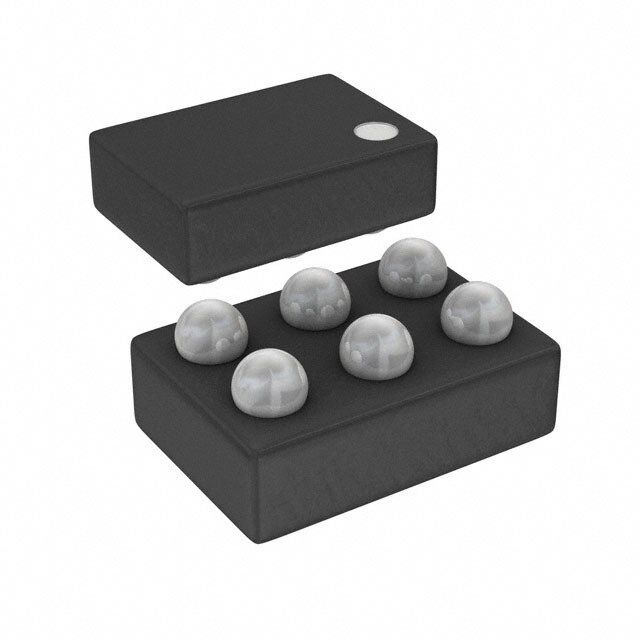
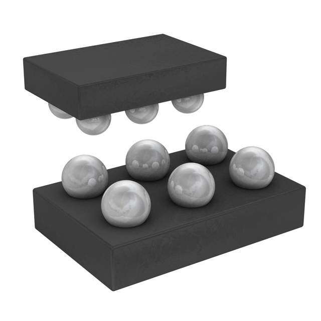
| 封装/外壳 | 6-UFBGA,CSPBGA |
| 封装/箱体 | WLCSP-6 |
| 工作温度范围 | - 40 C to + 85 C |
| 工作电源电压 | 3 V |
| 工厂包装数量 | 3000 |
| 带宽 | 3.5 GHz |
| 最小工作温度 | - 40 C |
| 标准包装 | 3,000 |
| 电压-电源 | 2.7 V ~ 5.5 V |
| 电流-电源 | 5.7mA |
| 电源电流 | 4.2 mA |
| 类型 | Log Amp Detector |
| 精度 | ±1dB |
| 系列 | AD8312 |
| 视频文件 | http://www.digikey.cn/classic/video.aspx?PlayerID=1364138032001&width=640&height=505&videoID=2245193150001 |
| 输入电压范围—最大 | 224 mV |
| 输入范围 | -45dBm ~ 0dBm |
| 通道数量 | 1 Channel |
| 频率 | 50MHz ~ 3.5GHz |


- 商务部:美国ITC正式对集成电路等产品启动337调查
- 曝三星4nm工艺存在良率问题 高通将骁龙8 Gen1或转产台积电
- 太阳诱电将投资9.5亿元在常州建新厂生产MLCC 预计2023年完工
- 英特尔发布欧洲新工厂建设计划 深化IDM 2.0 战略
- 台积电先进制程称霸业界 有大客户加持明年业绩稳了
- 达到5530亿美元!SIA预计今年全球半导体销售额将创下新高
- 英特尔拟将自动驾驶子公司Mobileye上市 估值或超500亿美元
- 三星加码芯片和SET,合并消费电子和移动部门,撤换高东真等 CEO
- 三星电子宣布重大人事变动 还合并消费电子和移动部门
- 海关总署:前11个月进口集成电路产品价值2.52万亿元 增长14.8%


PDF Datasheet 数据手册内容提取
50 MHz to 3.5 GHz, 45 dB RF Detector Data Sheet AD8312 FEATURES GENERAL DESCRIPTION Complete RF detector function The AD8312 is a complete, low cost subsystem for the Typical range: −45 dBm to 0 dBm, referencing 50 Ω measurement of radio frequency (RF) signals in the frequency Frequency response from 50 MHz to 3.5 GHz range of 50 MHz to 3.5 GHz. It has a typical dynamic range of Temperature stable linear in dB response 45 dB and is intended for use in a wide variety of cellular handsets Accurate to 3.5 GHz and other wireless devices. It provides a wider dynamic range Rapid response: 85/120 ns (rise/fall) and better accuracy than possible using discrete diode detectors. In Low power: 12 mW at 2.7 V particular, its temperature stability is excellent over the full operating range of −40°C to +85°C. Its high sensitivity allows APPLICATIONS measurement at low power levels, thus reducing the amount of Cellular handsets (GSM, CDMA, WCDMA) power that needs to be coupled to the detector. It is essentially a RSSI and TSSI for wireless terminal devices voltage responding device, with a typical signal range of 1.25 mV Transmitter power measurement to 224 mV rms or −45 dBm to 0 dBm, referencing 50 Ω. For convenience, the signal is internally ac-coupled, using a 5 pF capacitor to a load of 3 kΩ in shunt with 1.3 pF. This high- pass coupling, with a corner at approximately 16 MHz, determines the lowest operating frequency. Therefore, the source may be dc grounded. The AD8312 output, VOUT, increases from close to ground to about 1.2 V because the input signal level increases from 1.25 mV to 224 mV. A capacitor may be connected between the VOUT and CFLT pins when it is desirable to increase the time interval over which averaging of the input waveform occurs. The AD8312 is available in a 6-ball, 1.0 mm × 1.5 mm, wafer level chip scale package and consumes 4.2 mA from a 2.7 V to 5.5 V supply. FUNCTIONAL BLOCK DIAGRAM CFLT V-I VSET – + I-V VOUT DET DET DET DET DET RFIN BAND-GAP 10dB 10dB 10dB 10dB VPOS REFERENCE OFFSET COMM COMPENSATION AD8312 05260-001 Figure 1. Rev. B Document Feedback Information furnished by Analog Devices is believed to be accurate and reliable. However, no responsibility is assumed by Analog Devices for its use, nor for any infringements of patents or other One Technology Way, P.O. Box 9106, Norwood, MA 02062-9106, U.S.A. rights of third parties that may result from its use. Specifications subject to change without notice. No license is granted by implication or otherwise under any patent or patent rights of Analog Devices. Tel: 781.329.4700 ©2005–2015 Analog Devices, Inc. All rights reserved. Trademarks and registered trademarks are the property of their respective owners. Technical Support www.analog.com
AD8312 Data Sheet TABLE OF CONTENTS Features .............................................................................................. 1 Transfer Function in Terms of Slope and Intercept ............... 13 Applications ....................................................................................... 1 Filter Capacitor ....................................................................... 14 General Description ......................................................................... 1 Input Coupling Options ........................................................ 14 Functional Block Diagram .............................................................. 1 Increasing the Logarithmic Slope ........................................ 15 Revision History ............................................................................... 2 Effect of Waveform Type on Intercept ................................ 15 Specifications ..................................................................................... 3 Temperature Drift .................................................................. 16 Absolute Maximum Ratings ............................................................ 6 Operation Above 2.5 GHz .................................................... 16 ESD Caution .................................................................................. 6 Device Handling ..................................................................... 16 Pin Configuration and Function Descriptions ............................. 7 Evaluation Board .................................................................... 16 Typical Performance Characteristics ............................................. 8 Outline Dimensions ....................................................................... 19 General Description ....................................................................... 12 Ordering Guide .......................................................................... 19 Applications ..................................................................................... 13 Basic Connections ...................................................................... 13 REVISION HISTORY 12/15—Rev. A to Rev. B Change to Figure 30 Caption ........................................................ 16 1/11—Rev. 0 to Rev. A Changes to Figure 29 ...................................................................... 16 Updated Outline Dimensions ....................................................... 19 Changes to Ordering Guide .......................................................... 19 4/05—Revision 0: Initial Version Rev. B | Page 2 of 20
Data Sheet AD8312 SPECIFICATIONS V = 3 V, CFLT = open, T = 25°C, light condition = 600 LUX, 52.3 Ω termination resistor at RFIN, unless otherwise noted. S A Table 1. Parameter Test Conditions/Comments Min Typ Max Unit SIGNAL INPUT INTERFACE RFIN (Pin 6) Specified Frequency Range 0.05 3.5 GHz Input Voltage Range Internally ac-coupled 1.25 224 mV rms Equivalent Power Range 52.3 Ω external termination −45 0 dBm DC Resistance to COMM 100 kΩ MEASUREMENT MODE VOUT (Pin 2) shorted to VSET (Pin 3), sinusoidal input signal f = 50 MHz Input Impedance 3050 || 1.4 Ω || pF ±1 dB Dynamic Range T = 25°C 50 dB A −40°C < T < +85°C 42 dB A Maximum Input Level ±1 dB error 3 dBm Minimum Input Level ±1 dB error −47 dBm Slope 20.25 mV/dB Intercept −51.5 dBm Output Voltage—High Power In P = −10 dBm 0.841 V IN Output Voltage—Low Power In P = −40 dBm 0.232 V IN Temperature Sensitivity P = −10 dBm IN 25°C ≤ T ≤ +85°C 0.0010 dB/°C A −40°C ≤ T ≤ +25°C 0.0073 dB/°C A f = 100 MHz Input Impedance 2900 || 1.3 Ω || pF ±1 dB Dynamic Range T = 25°C 48 dB A −40°C < T < +85°C 40 dB A Maximum Input Level ±1 dB error 2 dBm Minimum Input Level ±1 dB error −46 dBm Slope 19.0 21.0 23.0 mV/dB Intercept −56.0 −50.5 −47.0 dBm Output Voltage—High Power In P = −10 dBm 0.850 V IN Output Voltage—Low Power In P = −40 dBm 0.222 V IN Temperature Sensitivity P = −10 dBm IN 25°C ≤ T ≤ +85°C 0.0002 dB/°C A −40°C ≤ T ≤ +25°C 0.0060 dB/°C A f = 900 MHz Input Impedance 890 || 1.15 Ω || pF ±1 dB Dynamic Range T = 25°C 49 dB A −40°C < T < +85°C 42 dB A Maximum Input Level ±1 dB error 1 dBm Minimum Input Level ±1 dB error −48.0 dBm Slope 20.25 mV/dB Intercept −51.9 dBm Output Voltage—High Power In P = −10 dBm 0.847 V IN Output Voltage—Low Power In P = −40 dBm 0.237 V IN Temperature Sensitivity P = −10 dBm IN 25°C ≤ T ≤ 85°C 0.0019 dB/°C A −40°C ≤ T ≤ +25°C 0.0010 dB/°C A Rev. B | Page 3 of 20
AD8312 Data Sheet Parameter Test Conditions/Comments Min Typ Max Unit f = 1.9 GHz Input Impedance 450 || 1.13 Ω || pF ±1 dB Dynamic Range T = 25°C 48 dB A −40°C < T < +85°C 40 dB A Maximum Input Level ±1 dB error 1 dBm Minimum Input Level ±1 dB error −47 dBm Slope 19.47 mV/dB Intercept −52.4 dBm Output Voltage − High Power In P = −10 dBm 0.826 V IN Output Voltage − Low Power In P = −40 dBm 0.240 V IN Temperature Sensitivity P = −10 dBm IN 25°C ≤ T ≤ 85°C 0.004 dB/°C A −40°C ≤ T ≤ +25°C 0.005 dB/°C A f = 2.2 GHz Input Impedance 430 || 1.09 Ω || pF ±1 dB Dynamic Range T = 25°C 48 dB A −40°C < T < +85°C 40 dB A Maximum Input Level ±1 dB error 1 dBm Minimum Input Level ±1 dB error −47 dBm Slope 19.1 mV/dB Intercept −52.1 dBm Output Voltage—High Power In P = −10 dBm 0.803 V IN Output Voltage—Low Power In P = −40 dBm 0.230 V IN Temperature Sensitivity P = −10 dBm IN 25°C ≤ T ≤ 85°C −0.0023 dB/°C A −40°C ≤ T ≤ +25°C 0.0055 dB/°C A f = 2.5 GHz Input Impedance 400 || 1.03 Ω || pF ±1 dB Dynamic Range T = 25°C 49 dB A −40°C < T < +85°C 40 dB A Maximum Input Level ±1 dB error 1 dBm Minimum Input Level ±1 dB error −48 dBm Slope 18.6 mV/dB Intercept −51.2 dBm Output Voltage—High Power In P = −10 dBm 0.762 V IN Output Voltage—Low Power In P = −40 dBm 0.204 V IN Temperature Sensitivity P = −10 dBm IN 25°C ≤ T ≤ 85°C 0.005 dB/°C A −40°C ≤ T ≤ +25°C −0.0126 dB/°C A OUTPUT INTERFACE VOUT (Pin 2) Minimum Output Voltage No signal at RFIN, R ≥ 10 kΩ 0.02 0.2 V L Maximum Output Voltage1 R ≥ 10 kΩ 1.8 2.0 V L General Limit 2.7 V ≤ V ≤ 5.5 V V − 1.2 V − 1 V S S S Available Output Current Sourcing/sinking 2/0.1 mA Residual RF (at 2f) f = 0.1 GHz (worst condition) 100 µV Output Noise RF input = 2.2 GHz, −10 dBm, f = 100 kHz, CFLT open 1.4 µV/√Hz NOISE Fall Time Input level = off to 0 dBm, 90% to 10% 120 ns Rise Time Input level = 0 dBm to off, 10% to 90% 85 ns VSET INTERFACE VSET (Pin 3) Input Resistance 13 kΩ Bias Current Source RFIN = −10 dBm; VSET = 1.2 V 75 µA Rev. B | Page 4 of 20
Data Sheet AD8312 Parameter Test Conditions/Comments Min Typ Max Unit POWER INTERFACE VPOS (Pin 1) Supply Voltage 2.7 3.0 5.5 V Quiescent Current 2.8 4.2 5.7 mA vs. Temperature −40°C ≤ T ≤ +85°C 4.3 mA A 1 Increased output is possible when using an attenuator between VOUT and VSET to raise the slope. Rev. B | Page 5 of 20
AD8312 Data Sheet ABSOLUTE MAXIMUM RATINGS Stresses at or above those listed under Absolute Maximum Table 2. Ratings may cause permanent damage to the product. This is a Parameter Value stress rating only; functional operation of the product at these Supply Voltage VPOS 5.5 V or any other conditions above those indicated in the operational VOUT, VSET 0 V, VPOS section of this specification is not implied. Operation beyond Input Voltage 1.6 V rms the maximum operating conditions for extended periods may Equivalent Power 17 dBm affect product reliability. Internal Power Dissipation 200 mW θ (WLCSP) 200°C/W ESD CAUTION JA Maximum Junction Temperature 125°C Operating Temperature Range −40°C to +85°C Storage Temperature Range −65°C to +150°C Rev. B | Page 6 of 20
Data Sheet AD8312 PIN CONFIGURATION AND FUNCTION DESCRIPTIONS AD8312 VPOS 1 6 RFIN VOUT 2 5 COMM VSET 3 4 CFLT (NToOt Pto V SIEcaWle) 05260-002 Figure 2. Pin Configuration Table 3. Pin Function Descriptions Ball No. Mnemonic Description 1 VPOS Positive Supply Voltage (V), 2.7 V to 5.5 V. S 2 VOUT Logarithmic Output. Output voltage increases with increasing input amplitude. 3 VSET Setpoint Input. Connect VSET to VOUT for measurement mode operation. The nominal logarithmic slope of 20 mV/dB can be increased to an arbitrarily high value by attenuating the signal between VOUT and VSET (see the Increasing the Logarithmic Slope section). 4 CFLT Connection for an External Capacitor to Slow the Response of the Output. Capacitor is connected between CFLT and VOUT. 5 COMM Device Common (Ground). 6 RFIN RF Input. Rev. B | Page 7 of 20
AD8312 Data Sheet TYPICAL PERFORMANCE CHARACTERISTICS V = 3 V; T = 25°C; C = open; light condition = 600 LUX, 52.3 Ω termination; unless otherwise noted. Colors: +25°C = black, S A FLT −40°C = blue, +85°C = red. 1.25 2.5 1.25 2.5 +85°C +85°C +25°C 2.0 +25°C 2.0 –40°C –40°C 1.00 1.5 1.00 1.5 1.0 1.0 V) 0.75 0.5 dB) V) 0.75 0.5 dB) UT ( 0 OR ( UT ( 0 OR ( O R O R V R V R 0.50 –0.5 E 0.50 –0.5 E –1.0 –1.0 0.25 –1.5 0.25 –1.5 0 ––22..50 05260-003 0 ––22..50 05260-006 –60 –50 –40 –30 –20 –10 0 10 –60 –50 –40 –30 –20 –10 0 10 PIN (dBm) PIN (dBm) Figure 3. VOUT and Logarithmic Conformance vs. Input Amplitude at 50 MHz; Figure 6. VOUT and Logarithmic Conformance vs. Input Amplitude at 1.9 GHz; Typical Device at −40°C, +25°C, and +85°C Typical Device at −40°C, +25°C, and +85°C 1.25 2.5 1.25 2.5 +85°C +85°C +25°C 2.0 +25°C 2.0 –40°C –40°C 1.00 1.5 1.00 1.5 1.0 1.0 V) 0.75 0.5 dB) V) 0.75 0.5 dB) UT ( 0 OR ( UT ( 0 OR ( O R O R V R V R 0.50 –0.5 E 0.50 –0.5 E –1.0 –1.0 0.25 –1.5 0.25 –1.5 0 ––22..50 05260-004 0 ––22..50 05260-007 –60 –50 –40 –30 –20 –10 0 10 –60 –50 –40 –30 –20 –10 0 10 PIN (dBm) PIN (dBm) Figure 4. VOUT and Logarithmic Conformance vs. Input Amplitude at 100 MHz; Figure 7. VOUT and Logarithmic Conformance vs. Input Amplitude at 2.2 GHz; Typical Device at −40°C, +25°C, and +85°C Typical Device at −40°C, +25°C, and +85°C 1.25 2.5 1.25 2.5 +85°C +85°C +25°C 2.0 +25°C 2.0 –40°C –40°C 1.00 1.5 1.00 1.5 1.0 1.0 V) 0.75 0.5 dB) V) 0.75 0.5 dB) UT ( 0 OR ( UT ( 0 OR ( O R O R V 0.50 –0.5 ER V 0.50 –0.5 ER –1.0 –1.0 0.25 –1.5 0.25 –1.5 0 ––22..50 05260-005 0 ––22..50 05260-008 –60 –50 –40 –30 –20 –10 0 10 –60 –50 –40 –30 –20 –10 0 10 PIN (dBm) PIN (dBm) Figure 5. VOUT and Logarithmic Conformance vs. Input Amplitude at 900 MHz; Figure 8. VOUT and Logarithmic Conformance vs. Input Amplitude at 2.5 GHz; Typical Device at −40°C, +25°C, and +85°C Typical Device at −40°C, +25°C, and +85°C Rev. B | Page 8 of 20
Data Sheet AD8312 2.5 2.5 +85°C +85°C 2.0 +25°C 2.0 +25°C –40°C –40°C 1.5 1.5 1.0 1.0 B) 0.5 B) 0.5 d d OR ( 0 OR ( 0 R R R R E –0.5 E –0.5 –1.0 –1.0 –1.5 –1.5 ––22..50 05260-009 ––22..50 05260-012 –60 –50 –40 –30 –20 –10 0 10 –60 –50 –40 –30 –20 –10 0 10 PIN (dBm) PIN (dBm) Figure 9. Distribution of Error at −40°C, +25°C, and +85°C After Ambient Figure 12. Distribution of Error at −40°C, +25°C, and +85°C After Ambient Normalization vs. Input Amplitude at 50 MHz for 80 Devices Normalization vs. Input Amplitude at 1.9 GHz for 80 Devices 2.5 2.5 +85°C +85°C 2.0 +25°C 2.0 +25°C –40°C –40°C 1.5 1.5 1.0 1.0 B) 0.5 B) 0.5 d d OR ( 0 OR ( 0 R R R R E –0.5 E –0.5 –1.0 –1.0 –1.5 –1.5 ––22..50 05260-010 ––22..05 05260-013 –60 –50 –40 –30 –20 –10 0 10 –60 –50 –40 –30 –20 –10 0 10 PIN (dBm) PIN (dBm) Figure 10. Distribution of Error at −40°C, +25°C, and +85°C After Ambient Figure 13. Distribution of Error at −40°C, +25°C, and +85°C After Ambient Normalization vs. Input Amplitude at 100 MHz for 80 Devices Normalization vs. Input Amplitude at 2.2 GHz for 80 Devices 2.5 2.5 +85°C +85°C 2.0 +25°C 2.0 +25°C –40°C –40°C 1.5 1.5 1.0 1.0 B) 0.5 B) 0.5 d d OR ( 0 OR ( 0 R R R R E –0.5 E –0.5 –1.0 –1.0 –1.5 –1.5 ––22..50 05260-011 ––22..50 05260-014 –60 –50 –40 –30 –20 –10 0 10 –60 –50 –40 –30 –20 –10 0 10 PIN (dBm) PIN (dBm) Figure 11. Distribution of Error at −40°C, +25°C, and +85°C After Ambient Figure 14. Distribution of Error at −40°C, +25°C, and +85°C After Ambient Normalization vs. Input Amplitude at 900 MHz for 80 Devices Normalization vs. Input Amplitude at 2.5 GHz for 80 Devices Rev. B | Page 9 of 20
AD8312 Data Sheet 100ns/HORIZ DIV RISE TIME 85ns FALL TIME 120ns 500mV/ VOUT 500mV/VERT DIV VERT DIV VOUT PULSED RF RF INPUT 0.1GHz, 0dBm VPOS 2V/VERT DIV 200mV/VERT DIV 05260-015 1s/HORIZ DIV 05260-018 Figure 15. VOUT Response Time, RF Off to 0 dBm Figure 18. Power-On and Power-Off Response RSMOHT0D6E G &E SNCEHRWATAORRZ TRIG OUT HP8648B 1R0EMFH OzUTPUT TERXIGT HPPU8L1S16EA TORUITG PULSE MODULATION SIGNAL GENERATOR GENERATOR PULSE RF OUT 20dBm RF OUT OUT +3dB RF –3dB AD811 49.9 SPLITTER AD8312 –3dB 732 3V 1 VPOS RFIN 6 0.1F 52.3 AD8312 2 VOUT COMM 5 1 VPOS RFIN 6 3 VSET CFLT 4 NC CH3* TRIG 52.3 2 VOUT COMM 5 TEKTRONIX NC = NO CONNECT CH1 TDS51504 *50 TSECROMPINEATION 05260-016 3NCV =S E NTO COCNFNLETCT4 NTFCEEKTP T6PR2R0OO4NBIEX TETSKDCTSOR78PO4TENCRIXIG 05260-019 Figure 16. Test Setup for Pulse Response Figure 19. Test Setup for Power-On and Power-Off Response +j1 10k +j0.5 +j2 z) H +j0.2 V/ 1k n Y ( T SI N E D L 100 0 A 0.2 0.5 1 2 0.1GHz TR C PE 0dBm E S 10 –10dBm S –20dBm 0.9GHz OI –j0.2 N –40dBm –j0.5 3.52G.5H–Gzj1Hz2.2GHz1.9GH–zj2 05260-017 1 1 3 10 FR30EQUE1N00CY (k3H00z) 1k 3–Rk6F0 OdBF1Fm0k 05260-020 Figure 17. Input Impedance vs. Frequency; No Termination Resistor on RFIN Figure 20. Noise Spectral Density of Output; CFLT = Open Rev. B | Page 10 of 20
Data Sheet AD8312 Table 4. Typical Specifications at Selected Frequencies at 25°C (Mean and Σ) ±1 dB Dynamic Range1 (dBm) Slope (mV/dB) Intercept (dBm) High Point Low Point Frequency (GHz) µ σ µ σ µ σ µ σ 0.05 20.25 0.3 −51.5 0.4 +3.0 0.12 −48.0 0.13 0.1 21.0 0.2 −50.5 0.4 +2.0 0.1 −46.0 0.1 0.9 20.25 0.3 −51.9 0.4 +0.2 0.1 −49.0 0.2 1.9 19.47 0.3 −52.4 0.6 +1.5 0.12 −48.8 0.3 2.2 19.1 0.4 −52.1 0.85 +1.5 0.2 −48.5 0.4 2.5 18.6 0.6 −51.2 1.2 +2.0 0.3 −47.7 0.5 3.0 17.5 0.7 −46.9 2.5 −4 0.3 −46 0.4 3.5 17.1 0.7 −42.6 2.5 −1 0.3 −39 0.3 1 Refer to Figure 23. Rev. B | Page 11 of 20
AD8312 Data Sheet GENERAL DESCRIPTION The AD8312 is a logarithmic amplifier similar in design to the In measurement modes, this output is connected back to a AD8313; further details about the structure and function may be voltage-to-current (V-to-I) stage, in such a manner that VOUT found in the AD8313 data sheet and the data sheets of other is a logarithmic measure of the RF input voltage with a slope logarithmic amplifiers produced by Analog Devices, Inc., Figure 21 and intercept controlled by the design. For a fixed termination shows the main features of the AD8312 in block schematic form. resistance at the input of the AD8312, a given voltage corresponds to a certain power level. The AD8312 combines two key functions needed for the measurement of signal level over a moderately wide dynamic range. The external termination added before the AD8312 determines First, it provides the amplification needed to respond to small the effective power scaling. This often takes the form of a simple signals in a chain of four amplifier/limiter cells, each having a small resistor (52.3 Ω provides a net 50 Ω input), but more elaborate signal gain of 10 dB and a bandwidth of approximately 3.5 GHz. matching networks may be used. This impedance determines the At the output of each amplifier stage is a full wave rectifier, essen- logarithmic intercept, the input power for which the output would tially a square law detector cell, which converts the RF signal cross the baseline (VOUT = 0) if the function were continuous voltages to a fluctuating current with an average value that for all values of input. Since this is never the case for a practical increases with signal level. A further passive detector stage is logarithmic amplifiers, the intercept refers to the value obtained added ahead of the first stage. Therefore, there are five detectors, by the minimum error, straight line fit to the actual graph of VOUT each separated by 10 dB, spanning some 50 dB of dynamic range. vs. input power. The quoted values assume a sinusoidal (CW) The overall accuracy at the extremes of this total range, viewed signal. Where there is complex modulation, as in CDMA, the as the deviation from an ideal logarithmic response, that is, the calibration of the power response needs to be adjusted accordingly. law conformance error, can be judged by reference to Figure 3 Where a true power (waveform independent) response is needed, through Figure 8, which show that errors across the central 40 dB the use of an rms responding detector, such as the AD8361, are moderate. These figures show how the conformance to an ideal should be considered. logarithmic function varies with temperature and frequency. However, in terms of the logarithmic slope, the amount by which The output of these detector cells is in the form of a differential the output VOUT changes for each decibel of input change (voltage current, making their summation a simple matter. It can easily or power), is, in principle, independent of waveform or termination be shown that such summation closely approximates a logarithmic impedance. In practice, it usually falls off at higher frequencies function. This result is then converted to a voltage at the VOUT because of the declining gain of the amplifier stages and other pin through a high gain stage. effects in the detector cells. For the AD8312, the slope at low frequencies is nominally 21.0 mV/dB, falling almost linearly with frequency to about 18.6 mV/dB at 2.5 GHz. These values are sensibly independent of temperature and almost totally unaffected by supply voltages of 2.7 V to 5.5 V. CFLT V-I VSET – + I-V VOUT DET DET DET DET DET RFIN BAND-GAP 10dB 10dB 10dB 10dB VPOS REFERENCE OFFSET COMM COMPENSATION AD8312 05260-021 Figure 21. Block Schematic Rev. B | Page 12 of 20
Data Sheet AD8312 APPLICATIONS INFORMATION BASIC CONNECTIONS 1.2 3 VS= 2.7V Figure 22 shows the basic connections for measurement mode. RT = 52.3 1.0 2 A supply voltage of 2.7 V to 5.5 V is required. The supply to the 1dB DYNAMIC RANGE VPOS pin should be decoupled with a low inductance 0.1 μF surface-mount ceramic capacitor. A series resistor of about 10 Ω 0.8 1 may be added; this resistor slightly reduces the supply voltage to the V) dB) AD8312 (maximum current into the VPOS pin is approximately UT ( 0.6 0 OR ( O R 5.7 mA). Its use should be avoided in applications where the power V R E supply voltage is very low (that is, 2.7 V). A series inductor 0.4 –1 provides similar power supply filtering with minimal drop in supply voltage. 0.2 –2 0.1F 52.3 0 INTER3CdEBP DTYNAMIC RANGE –3 05260-023 AD8312 –60 –50 –40 –30 –20 –10 0 10 VS 1 VPOS RFIN 6 INPUT PIN (dBm) OPTIONAL Figure 23. VOUT and Logarithmic Conformance Error vs. (SEE TEXT) Input Level vs. Input Level at 900 MHz VOUT 2 VOUT COMM 5 TRANSFER FUNCTION IN TERMS OF SLOPE AND 3 VSET CFLT 4 INTERCEPT CF The transfer function of the AD8312 is characterized in terms (OSPETEI OTENXATL) 05260-022 ochf aitnsg selo ipne t haen dR SinStIe orcuetpptu. tT vhoelt laoggea froitrh am 1i cd sBlo cphea nisg de eafti nthede iansp tuhte. Figure 22. Basic Connections for Operation in Measurement Mode For the AD8312, the slope is nominally 20 mV/dB. Therefore, a 10 dB change at the input results in a change at the output of The AD8312 has an internal input coupling capacitor. This approximately 200 mV. Figure 23 shows the range over which eliminates the need for external ac coupling. In this example, a the device maintains its constant slope. The dynamic range can broadband input match is achieved by connecting a 52.3 Ω resistor be defined as the range over which the error remains within a between RFIN and ground. This resistance combines with the certain band, usually ±1 dB or ±3 dB. In Figure 23, for example, internal input impedance of approximately 3 kΩ to give an overall the ±1 dB dynamic range is approximately 51 dB (from −49 dBm broadband input resistance of 50 Ω. Several other coupling to +2 dBm). methods are possible; these are described in the Input Coupling Options section. The intercept is the point at which the extrapolated linear response would intersect the horizontal axis (see Figure 23). Using the slope The measurement mode is selected by connecting VSET to VOUT, and intercept, the output voltage can be calculated for any input which establishes a feedback path and sets the logarithmic slope to level within the specified input range by its nominal value. The peak voltage range of the measurement extends from −49 dBm to 0 dBm at 0.9 GHz and is only slightly VOUTV (P P ) SLOPE IN O less at higher frequencies up to 2.5 GHz. At a slope of 21.0 mV/dB, where: this would amount to an output span of 1.029 V. Figure 23 shows the transfer function for VOUT at a supply voltage of 2.7 V and VOUT is the demodulated and filtered RSSI output. an input frequency of 900 MHz. VSLOPE is the logarithmic slope, expressed in V/dB. P is the input signal, expressed in decibels relative to some IN The load resistance on VOUT should not be lower than 4 kΩ so reference level (dBm in this case). that the full-scale output can be generated with the limited available P is the logarithmic intercept, expressed in decibels relative to O current of 1 mA maximum. Figure 23 shows the logarithmic the same reference level. conformance under the same conditions. For example, at an input level of −27 dBm, the output voltage is VOUT 0.020V/dB[27dBm(50dBm)]0.46V Rev. B | Page 13 of 20
AD8312 Data Sheet Filter Capacitor The impedance matching characteristics of a reactive matching network provide voltage gain ahead of the AD8312, which The video bandwidth of VOUT is approximately 3.5 MHz. In CW increases device sensitivity (see Table 5). The voltage gain is applications where the input frequency is much higher than this, calculated by no further filtering of the demodulated signal is required. Where there is a low frequency modulation of the carrier amplitude, R2 however, the low pass corner must be reduced by the addition VoltageGaindB =20log10 R1 of an external filter capacitor, C (see Figure 22). The video F where: bandwidth is related to C by F R2 is the input impedance of the AD8312. 1 VideoBandwidth= R1 is the source impedance to which the AD8312 is being 2π×13kΩ×(3.5pF+C ) F matched. Input Coupling Options Note that this gain is only achieved for a perfect match. Component The internal 5 pF coupling capacitor of the AD8312, along with tolerances and the use of standard values tend to reduce gain. the low frequency input impedance of 3 kΩ, gives a high pass 50Ω SOURCE AD8312 input corner frequency of approximately 16 MHz. This sets the minimum operating frequency. Figure 24 to Figure 26 show 50Ω RFIN three options for input coupling. A broadband resistive match RSHUNT CC can be implemented by connecting a shunt resistor to ground at 52.3Ω CIN RIN RbeF IuNse (ds etoe Fseigleucrte d 2if4f)e.r Tenhti so 5v2er.3a lΩl i nrepsuist tiomr p(oedthaenrc veas)lu ceosm cabnin aelss o VBIAS 05260-024 with the input impedance of the AD8312 (2.9 kΩ || 1.3 pF) to Figure 24. Broadband Resistive Method for Input Coupling give a broadband input impedance of 50 Ω. While the input resistance and capacitance (R and C ) varies by approximately IN IN ±20% from device to device, the dominance of the external 50Ω SOURCE AD8312 shunt resistor means that the variation in the overall input 50Ω X1 RFIN impedance is close to the tolerance of the external resistor. CC X2 At frequencies above 2 GHz, the input impedance drops below CIN RIN 4va5l0u Ωe. ;T thhiesr evfaolruee, iist icsa alcpuplraotepdr ibatye p tloo tutsine ga tlhareg ienrp suhtu inmt preedsiasntocre VBIAS 05260-025 (resistance and capacitance) on a Smith Chart and by choosing Figure 25. Narrow-Band Reactive Method for Input Coupling the best shunt resistor value to bring the input impedance closest to the center of the chart (see Figure 17). At 2.5 GHz, a shunt resistor AD8312 of 57.6 Ω is recommended. RFIN A reactive match can also be implemented as shown in Figure 25. This is not recommended at low frequencies because device STRIPLINE RATTN CC tolerances dramatically vary the quality of the match due to the CIN RIN lias rrgeec oinmpmute rnedsiesdta. nce. For low frequencies, Figure 24 or Figure 26 VBIAS 05260-026 In Figure 25, the matching components are drawn as general Figure 26. Series Attenuation Method for Input Coupling reactances. Depending on the frequency, the input impedance at Figure 26 shows a third method for coupling the input signal that frequency and the availability of standard value components, into the AD8312, which is applicable in applications where the either a capacitor or an inductor, is used. As in the previous case, input signal is larger than the input range of the logarithmic the input impedance at a particular frequency is plotted on a amplifier. A series resistor, connected to the RF source, combines Smith Chart and matching components are chosen (Shunt or with the input impedance of the AD8312 to resistively divide Series L, or Shunt or Series C) to move the impedance to the the input signal being applied to the input. This has the advantage center of the chart. Matching components for specific frequencies of very little power being tapped off in RF power transmission can be calculated using the Smith Chart (see Figure 17). Table 5 applications. outlines the input impedances for some commonly used frequencies. Rev. B | Page 14 of 20
Data Sheet AD8312 4.0 Table 5. Input Impedance for Select Frequency Frequency S11 Impedance Ω 3.5 (GHz) Real Imaginary (Series) 0.05 0.967 −0.043 1090 − j 1461 3.0 5.0V 0.1 0.962 −0.081 422.6 − j 1015 SUPPLY 2.5 0.9 0.728 −0.535 25.6 − j 148.5 V) 1.9 0.322 −0.891 11.5 − j 72.69 T ( 2.0 U 2.2 0.230 −0.832 9.91 − j 64.74 VO 3.0 1.5 2.7V 2.5 0.165 −0.845 9.16 − j 59.91 2.0 SUPPLY 3.0 0.126 −0.849 8.83 − j 57.21 1.0 3.5 0.146 −0.826 10.5 − j 58.54 1.0 Increasing the Logarithmic Slope 0.05 05260-028 The nominal logarithmic slope of 20 mV/dB can be increased to –60 –50 –40 –30 –20 –10 0 10 an arbitrarily high value by attenuating the signal between VOUT PIN (dBm) and VSET, as shown in Figure 27. The ratio R1/R2 is set by Figure 28. VOUT vs. Input Level at Various Logarithmic Slopes Effect of Waveform Type on Intercept NewSlope R1/R2 1 OriginalSlope Although specified for input levels in dBm (dB relative to 1 mW), the AD8312 fundamentally responds to voltage and not to power. In the example shown, two 2 kΩ resistors combine to change the A direct consequence of this characteristic is that input signals slope at 1900 MHz from approximately 20 mV/dB to 40 mV/dB. of equal rms power but differing crest factors, produce different Note that R2 is in parallel with the input resistance of VSET, results at the output of the logarithmic amplifier. typically 13 kΩ. Therefore, the exact R1/R2 ration may vary. The effect of differing signal waveforms is to shift the effective value of the intercept upwards or downwards. Graphically, this AD8312 looks like a vertical shift in the logarithmic amplifier transfer ~40mV/dB VOUT @ 1900MHz function. The logarithmic slope, however, is not affected. For R1 2k example, consider the case of the AD8312 being alternately fed VSET R2k2 05260-027 bremqyu asi nvp aoulwennmetr o.o Tdf uh1l.ea6 t odeudBt sp(i3un1te mvwoaVlvt)ae go aevn eodrf btthyhe ea c A6o4mD Qp8Al3e1tMe2 d dsyiignfnfaeamrls oi cbf yrtah tneh gesea mofe Figure 27. Increasing the Output Slope the device (with the output for a 64 QAM input being lower). The slope can be increased to higher levels, as shown in Figure 28. Figure 29 shows the transfer function of the AD8312 when driven This, however, reduces the usable dynamic range of the device, by both an unmodulated sine wave and several different signal depending on the supply voltage. waveforms. For precision operation, the AD8312 should be Output loading should be considered when choosing resistor calibrated for each signal type that is driving it. To measure the values for slope adjustment to ensure proper output swing. Note rms power of a 64 QAM input, for example, the mV equivalent that the load resistance on VOUT should not be lower than 4 kΩ in of the dB value (19.47 mV/dB × 1.6 dB) should be subtracted order that the full-scale output can be generated with the limited from the output voltage of the AD8312. available current of 1 mA. Rev. B | Page 15 of 20
AD8312 Data Sheet 5 1.0 5 +85°C 4 0.9 +25°C 4 –40°C 3 0.8 3 2 0.7 2 B) 1 CW IS-95REV ERROR(d –10 OUT (V) 00..65 01 ROR (dB) V R 0.4 –1 E –2 0.3 –2 –3 WCDMA64-CH 64QAM ––54–60 –50 –40 –30 –20 –10 0 1005260-029 00..210 –––543 05260-031 INPUT(dBm) –55 –45 –35 –25 –15 –5 5 Figure 29. Shift in Transfer Function due to PIN (dBm) Several Different Signal Waveforms Figure 31.Output Voltage and Error at −40°C, +25°C, and +85°C after Temperature Drift Ambient Normalization vs. Input Amplitude at 3.0 GHz for 60 Devices Figure 30 shows the logarithmic slope and error over temperature 1.0 5 +85°C for a 0.9 GHz input signal. Error due to drift over temperature 0.9 +25°C 4 –40°C consistently remains within ±0.5 dB and only begins to exceed this 0.8 3 limit when the ambient temperature goes above 70°C. For all 0.7 2 frequencies using a reduced temperature range, higher meas- urement accuracy is achievable. V) 0.6 1 dB) 1.3 2.5 UT ( 0.5 0 OR ( O R V R 2.0 0.4 –1 E 1.0 1.5 0.3 –2 1.0 0.2 –3 UT (V) 0.8 00.5 OR (dB) 0.10 ––54 05260-032 O R –55 –45 –35 –25 –15 –5 5 V R 0.5 –0.5 E PIN (dBm) +85°C +70°C –1.0 Figure 32. Output Voltage and Error at −40°C, +25°C, and +85°C after +25°C Ambient Normalization vs. Input Amplitude at 3.5 GHz for 30 Devices 0.3 0°C –1.5 –10°C Device Handling 0 ––2400°°CC ––22..50 05260-030 The wafer level chip scale package consists of solder bumps –60 –50 –40 –30 –20 –10 0 10 connected to the active side of the die. The device is lead free with PIN (dBm) 95.5% tin, 4.0% silver, and 0.5% copper solder bump composition. Figure 30. Typical Drift at 900 MHz for Various Temperatures The WLCSP package can mount on printed circuit boards using Operation Above 2.5 GHz standard surface-mount assembly techniques. However, take caution to avoid damaging the die. See the AN-617 application The AD8312 works at high frequencies, but exhibits slightly note, Wafer Level Chip Scale Package, for additional information. higher output voltage temperature drift. Figure 31 and Figure 32 WLCSP devices are bumped die; exposed die can be sensitive to show the transfer functions and error distributions of a large light conditions, which can influence specified limits. population of devices at 3.0 GHz and 3.5 GHz over temperature. Evaluation Board Due to the repeatability of the drift from device to device, comp- ensation can be applied to reduce the effects of temperature drift. Figure 33 shows the schematic of the AD8312 evaluation board. In the case of the 3.5 GHz distribution, an intercept correction The layout and silkscreen of the component and circuit sides are of 2.0 dB at 85°C would improve the accuracy of the distribution shown in Figure 34 to Figure 37. The board is powered by a to ±2 dB over a +40 dB range. single supply in the 2.7 V to 5.5 V range. The power supply is decoupled by a single 0.1 µF capacitor. Table 6 details the various configuration options of the evaluation board. Rev. B | Page 16 of 20
Data Sheet AD8312 C2 0.1F R1 52.3 AD8312 VPOS 1 VPOS RFIN 6 INPUT R3 0 VOUT 2 VOUT COMM 5 C4 R8 R6 (OPEN) (OPEN) (OPEN) R4 0 3 VSET CFLT 4 R7 TO EDGE 0 CONNECTOR VSET R5 R2 (OPEN) (OPEN) C3 COTNON EEDCGTEOR (OPEN) 05260-033 Figure 33. Evaluation Board Schematic 05260-036 05260-037 Figure 34. Silkscreen of Component Side (WLCSP) Figure 36. Silkscreen of Circuit Side (WLCSP) 05260-034 05260-035 Figure 35. Layout of Component Side (WLCSP) Figure 37. Layout of Circuit Side (WLCSP) Rev. B | Page 17 of 20
AD8312 Data Sheet Table 6. Evaluation Board Configuration Options Default Component Function Condition VPOS, GND Supply and Ground Vector Pins. Not Applicable C2 Power Supply Decoupling. The nominal supply decoupling consists of a 0.1 µF capacitor (C1). C2 = 0.1 µF (Size 0603) R1 Input Interface. The 52.3 Ω resistor in Position R1 combines with the internal input impedance of the R1 = 52.3 Ω AD8312 to give a broadband input impedance of around 50 Ω. (Size 0603) R2, R4 Slope Adjust. By installing resistors in R2 and R4, the nominal slope of 20 mV/dB can be changed. See the R2 = Open Increasing the Logarithmic Slope section for more details. (Size 0402) R4 = 0 Ω (Size 0402) C3 Filter Capacitor. The response time of VOUT can be modified by placing a capacitor between CFLT (Pin 4) C3 = Open and VOUT (Pin 2). (Size 0603) R3, R8, C4 Output Interface. R3, R8, and C4 can be used to check the response of VOUT to capacitive and resistive R3 = 0 Ω loading. R3/R8 can be used to attenuate VOUT. (Size 0603) R8 = C4 = Open (Size 0402) R7 VSET Interface. R7 can be used to reduce capacitive loading from transmission lines. R7 = 0 Ω (Size 0603) R5, R6 Alternate Interface. R5 and R6 allow for VOUT and VSET to be accessible from the edge connector, which R5 = R6 = Open is only used for characterization. (Size 0402) Rev. B | Page 18 of 20
Data Sheet AD8312 OUTLINE DIMENSIONS 0.675 0.595 1.00 0.380 0.515 0.95 0.355 SEATING 0.90 0.330 PLANE 2 1 A A1BALL 0.345 CORNER 0.295 1.00 1.50 BSC 0.245 1.45 B 1.40 0.50 BSC C 0.075 TOPVIEW 0.270 COPLANARITY (BALLSIDEDOWN) 0.240 0.50BSC BOTTOMVIEW 0.210 (BALLSIDEUP) 081607-B Figure 38. 6-Ball Wafer-Level Chip Scale Package [WLCSP] (CB-6-2) Dimensions shown in millimeters ORDERING GUIDE Package Branding Ordering Model1 Temperature Range Package Description Outline Information Quantity AD8312ACBZ-P7 –40°C to +85°C 6-Ball WLCSP, 7” Pocket Tape and Reel CB-6-2 Q00 3000 AD8312ACBZ-P2 –40°C to +85°C 6-Ball WLCSP, 7” Pocket Tape and Reel CB-6-2 Q00 250 AD8312-EVALZ Evaluation Board 1 Z = RoHS Compliant Part. Rev. B | Page 19 of 20
AD8312 Data Sheet NOTES ©2005–2015 Analog Devices, Inc. All rights reserved. Trademarks and registered trademarks are the property of their respective owners. D05260-0-12/15(B) Rev. B | Page 20 of 20